

Page 1

WA_DEV_Q26RD_PTS_001
002
April 20, 2010
AirPrime Q2687 Refreshed
Product Technical Specification
and Customer Design Guideline
Page 2

Product Technical Specification and
Customer Design Guideline
Important Notice
Due to the nature of wireless communications, transmission and reception of data can never be
guaranteed. Data may be delayed, corrupted (i.e., have errors) or be totally lost. Although significant
delays or losses of data are rare when wireless devices such as the Sierra Wireless modem are used
in a normal manner with a well-constructed network, the Sierra Wireless modem should not be used
in situations where failure to transmit or receive data could result in damage of any kind to the user or
any other party, including but not limited to personal injury, death, or loss of property. Sierra Wireless
accepts no responsibility for damages of any kind resulting from delays or errors in data transmitted or
received using the Sierra Wireless modem, or for failure of the Sierra Wireless modem to transmit or
receive such data.
Safety and Hazards
Do not operate the Sierra Wireless modem in areas where blasting is in progress, where explosive
atmospheres may be present, near medical equipment, near life support equipment, or any equipment
which may be susceptible to any form of radio interference. In such areas, the Sierra Wireless modem
MUST BE POWERED OFF. The Sierra Wireless modem can transmit signals that could interfere with
this equipment. Do not operate the Sierra Wireless modem in any aircraft, whether the aircraft is on
the ground or in flight. In aircraft, the Sierra Wireless modem MUST BE POWERED OFF. When
operating, the Sierra Wireless modem can transmit signals that could interfere with various onboard
systems.
Note: Some airlines may permit the use of cellular phones while the aircraft is on the ground and the door is
open. Sierra Wireless modems may be used at this time.
The driver or operator of any vehicle should not operate the Sierra Wireless modem while in control of
a vehicle. Doing so will detract from the driver or operator’s control and operation of that vehicle. In
some states and provinces, operating such communications devices while in control of a vehicle is an
offence.
Limitations of Liability
This manual is provided “as is”. Sierra Wireless makes no warranties of any kind, either expressed or
implied, including any implied warranties of merchantability, fitness for a particular purpose, or
noninfringement. The recipient of the manual shall endorse all risks arising from its use.
The information in this manual is subject to change without notice and does not represent a
commitment on the part of Sierra Wireless. SIERRA WIRELESS AND ITS AFFILIATES
SPECIFICALLY DISCLAIM LIABILITY FOR ANY AND ALL DIRECT, INDIRECT, SPECIAL,
GENERAL, INCIDENTAL, CONSEQUENTIAL, PUNITIVE OR EXEMPLARY DAMAGES INCLUDING,
BUT NOT LIMITED TO, LOSS OF PROFITS OR REVENUE OR ANTICIPATED PROFITS OR
REVENUE ARISING OUT OF THE USE OR INABILITY TO USE ANY SIERRA WIRELESS
PRODUCT, EVEN IF SIERRA WIRELESS AND/OR ITS AFFILIATES HAS BEEN ADVISED OF THE
POSSIBILITY OF SUCH DAMAGES OR THEY ARE FORESEEABLE OR FOR CLAIMS BY ANY
THIRD PARTY.
Notwithstanding the foregoing, in no event shall Sierra Wireless and/or its affiliates aggregate liability
arising under or in connection with the Sierra Wireless product, regardless of the number of events,
occurrences, or claims giving rise to liability, be in excess of the price paid by the purchaser for the
Sierra Wireless product.
WA_DEV_Q26RD_PTS_001 Rev 002 April 20, 2010 2
Page 3

Product Technical Specification and
Customer Design Guideline
Patents
5,515,013
5,629,960
5,845,216
5,847,553
5,878,234
5,890,057
5,929,815
6,169,884
6,191,741
6,199,168
6,339,405
6,359,591
6,400,336
6,516,204
6,561,851
6,643,501
6,653,979
6,697,030
6,785,830
6,845,249
6,847,830
6,876,697
6,879,585
6,886,049
6,968,171
6,985,757
7,023,878
7,053,843
7,106,569
7,145,267
7,200,512
7,295,171
7,287,162
D442,170
D459,303
D599,256
D560,911
Sales Desk:
Phone:
1-604-232-1488
Hours:
8:00 AM to 5:00 PM Pacific Time
E-mail:
sales@sierrawireless.com
Post:
Sierra Wireless
13811 Wireless Way
Richmond, BC
Canada V6V 3A4
Fax:
1-604-231-1109
Web:
www.sierrawireless.com
Portions of this product may be covered by some or all of the following US patents:
and other patents pending.
This product includes technology licensed from QUALCOMM
®
3G
Manufactured or sold by Sierra Wireless or its licensees under one or more patents licensed from
InterDigital Group.
Copyright
© 2010 Sierra Wireless. All rights reserved.
Trademarks
AirCard® and Watcher® are registered trademarks of Sierra Wireless. Sierra Wireless™, AirPrime™,
AirLink™, AirVantage™ and the Sierra Wireless logo are trademarks of Sierra Wireless.
, , ®, inSIM®, WAVECOM®, WISMO®, Wireless Microprocessor®,
Wireless CPU®, Open AT® are filed or registered trademarks of Sierra Wireless S.A. in France and/or
in other countries.
Windows
®
and Windows Vista® are registered trademarks of Microsoft Corporation.
Macintosh and Mac OS are registered trademarks of Apple Inc., registered in the U.S. and other
countries.
QUALCOMM
®
is a registered trademark of QUALCOMM Incorporated. Used under license.
Other trademarks are the property of the respective owners.
Contact Information
Consult our website for up-to-date product descriptions, documentation, application notes, firmware
upgrades, troubleshooting tips, and press releases: www.sierrawireless.com
WA_DEV_Q26RD_PTS_001 Rev 002 April 20, 2010 3
Page 4

Product Technical Specification and
Customer Design Guideline
Document History
Version
Date
Updates
001
January 28, 2010
Creation
002
April 20, 2010
Reformatted in the rebranded SWI template.
In Section 3 Technical Specifications:
Moved the Power Supply Design Requirements to section 9.1
Power Supply
Updated Figure 5
In section 4 Interfaces:
Updated section 4.7.4 5-wire Serial Interface
Updated section 4.8.1 Pin Description
Updated section 4.8.3 4-wire Serial Interface
Updated section 8.4 Reliability Prediction Model.
Updated links in section 13.1.1 Web Site Support.
Updated Intelligent Embedded Module weight to 8g.
Updated the RF Component list.
Removed references to IMP Connector throughout the document.
Updated Figure 10 Example of a 4-wire SPI Bus Application.
Updated section 4.15 Temperature Sensor Interface.
Updated Power ON information based on Tracker 01626.
Updated U1 Chip information based on CUS57225.
Updated antenna gain information.
Updated FCC ID.
Updated power consumption values in section 6 Power Consumption.
Updated Figure 5 Q2687 Refreshed Embedded Module Mechanical Drawing
and Figure 6 Maximum Bulk Occupied on the Host Board.
WA_DEV_Q26RD_PTS_001 Rev 002 April 20, 2010 4
Page 5

Contents
1. INTRODUCTION ................................................................................................ 16
1.1. Physical Dimensions ................................................................................................... 16
1.2. General Features ........................................................................................................ 16
1.3. GSM/GPRS/EGPRS Features .................................................................................... 18
1.4. Interfaces ................................................................................................................... 18
1.5. Operating System ....................................................................................................... 18
1.6. Connection Interfaces ................................................................................................. 19
1.7. Environment and Mechanics ....................................................................................... 19
1.7.1. RoHS Directive Compliant ................................................................................... 19
1.7.2. Disposing of the Product ...................................................................................... 19
2. FUNCTIONAL SPECIFICATIONS ...................................................................... 20
2.1. Functional Architecture ............................................................................................... 20
2.1.1. RF Functionalities ................................................................................................ 20
2.1.2. Baseband Functionalities ..................................................................................... 21
2.2. Operating System ....................................................................................................... 21
3. TECHNICAL SPECIFICATIONS ........................................................................ 22
3.1. Power Supply ............................................................................................................. 22
3.1.1. Power Supply Pin-Out .......................................................................................... 23
3.1.2. Start-Up Current .................................................................................................. 24
3.1.3. Decoupling of Power Supply Signals .................................................................... 24
3.2. Mechanical Specifications ........................................................................................... 24
3.3. Firmware Upgrade ...................................................................................................... 27
4. INTERFACES ..................................................................................................... 28
4.1. General Purpose Connector (GPC) ............................................................................. 28
4.1.1. Pin Description .................................................................................................... 29
4.1.2. Pin Out Differences .............................................................................................. 34
4.2. Electrical Information for Digital I/O ............................................................................. 35
4.3. General Purpose Input/Output .................................................................................... 37
4.3.1. Pin Description .................................................................................................... 37
4.4. Serial Interface ........................................................................................................... 39
4.4.1. SPI Bus ............................................................................................................... 39
4.4.1.1. Characteristics ........................................................................................................ 39
4.4.1.2. SPI Configuration .................................................................................................... 39
4.4.1.3. SPI Waveforms ....................................................................................................... 40
4.4.1.4. SPI1 Pin Description ................................................................................................ 41
4.4.1.5. SPI2 Pin Description ................................................................................................ 41
4.4.1.6. Application .............................................................................................................. 42
4.4.2. I2C Bus ................................................................................................................ 43
4.4.2.1. I2C Waveforms ........................................................................................................ 43
4.4.2.2. I2C Pin Description .................................................................................................. 44
4.4.2.3. Application .............................................................................................................. 44
4.5. Parallel Interface ......................................................................................................... 45
WA_DEV_Q26RD_PTS_001 Rev 002 April 20, 2010 5
Page 6

Product Technical Specification and
Customer Design Guideline
4.5.1. Pin Description .................................................................................................... 45
4.5.2. Electrical Characteristics ...................................................................................... 46
4.5.3. Asynchronous Access .......................................................................................... 46
4.5.4. Synchronous Access ........................................................................................... 48
4.5.5. Additional Information Regarding Address Size Bus ............................................. 51
4.5.6. Application ........................................................................................................... 51
4.6. Keyboard Interface ..................................................................................................... 52
4.6.1. Pin Description .................................................................................................... 52
4.6.2. Application ........................................................................................................... 53
4.7. Main Serial Link (UART1) ........................................................................................... 54
4.7.1. Pin Description .................................................................................................... 54
4.7.2. Level Shifter Implementation ................................................................................ 55
4.7.2.1. Recommended Components .................................................................................... 55
4.7.3. V24/CMOS Possible Designs ............................................................................... 56
4.7.4. 5-wire Serial Interface .......................................................................................... 57
4.7.5. 4-wire Serial Interface .......................................................................................... 57
4.7.6. 2-wire Serial Interface .......................................................................................... 57
4.8. Auxiliary Serial Link (UART2) ...................................................................................... 58
4.8.1. Pin Description .................................................................................................... 58
4.8.2. Level Shifter Implementation ................................................................................ 59
4.8.2.1. Recommended Components .................................................................................... 59
4.8.3. 4-wire Serial Interface .......................................................................................... 60
4.8.4. 2-wire Serial Interface .......................................................................................... 60
4.9. SIM Interface .............................................................................................................. 61
4.9.1. Pin Description .................................................................................................... 61
4.9.2. Electrical Characteristics ...................................................................................... 61
4.9.3. Application ........................................................................................................... 62
4.9.3.1. SIM Socket Pin Description ...................................................................................... 62
4.9.3.2. Recommended Components .................................................................................... 63
4.10. USB 2.0 Interface ....................................................................................................... 64
4.10.1. Pin Description .................................................................................................... 64
4.10.2. Electrical Characteristics ...................................................................................... 64
4.10.3. Application ........................................................................................................... 65
4.10.3.1. Recommended Components .................................................................................. 65
4.11. RF Interface ................................................................................................................ 66
4.11.1. RF Connections ................................................................................................... 66
4.11.1.1. UFL Connector ...................................................................................................... 66
4.11.1.2. Soldered Solution .................................................................................................. 66
4.11.1.3. Precidip Connector ................................................................................................ 66
4.11.2. RF Performance .................................................................................................. 66
4.11.3. Antenna Specifications ........................................................................................ 67
4.11.3.1. Application ............................................................................................................ 67
4.12. Analog Audio Interface................................................................................................ 68
4.12.1. Pin Description .................................................................................................... 68
4.12.2. Microphone Features ........................................................................................... 68
4.12.2.1. MIC1 Microphone Input .......................................................................................... 68
4.12.2.2. MIC2 Microphone Input .......................................................................................... 72
4.12.3. Speaker Features ................................................................................................ 75
4.12.3.1. Speakers Output Power ......................................................................................... 76
4.12.3.2. SPK1 Speaker Output............................................................................................ 76
WA_DEV_Q26RD_PTS_001 Rev 002 April 20, 2010 6
Page 7

Product Technical Specification and
Customer Design Guideline
4.12.3.3. SPK2 Speaker Output............................................................................................ 77
4.12.3.4. Differential Connection Example ............................................................................ 78
4.12.3.5. Single-Ended Connection Example ........................................................................ 78
4.12.3.6. Recommended Characteristics .............................................................................. 79
4.13. Digital Audio Interface (PCM) ...................................................................................... 80
4.13.1. PCM Waveforms.................................................................................................. 81
4.13.2. Pin Description .................................................................................................... 82
4.14. Battery Charging Interface .......................................................................................... 83
4.14.1. Charging Algorithms ............................................................................................ 84
4.14.1.1. Ni-Cd/Ni-Mh Charging Algorithm ............................................................................ 84
4.14.1.2. Li-Ion Charging Algorithm ...................................................................................... 85
4.14.2. Pre-Charging ....................................................................................................... 88
4.14.3. Temperature Monitoring ....................................................................................... 88
4.14.4. Recharging .......................................................................................................... 88
4.14.5. Application ........................................................................................................... 89
4.14.5.1. Temperature Computation Method ......................................................................... 89
4.14.6. Charger Recommendations ................................................................................. 90
4.15. Temperature Sensor Interface .................................................................................... 91
5. SIGNALS AND INDICATORS ............................................................................ 92
5.1. ON/~OFF Signal ......................................................................................................... 92
5.1.1. Pin Description .................................................................................................... 92
5.1.2. Electrical Characteristics ...................................................................................... 92
5.1.3. Power-ON ............................................................................................................ 92
5.1.4. Power-OFF .......................................................................................................... 94
5.1.5. Application ........................................................................................................... 95
5.2. Reset Signal (~RESET) .............................................................................................. 96
5.2.1. Reset Sequence .................................................................................................. 96
5.2.2. Pin Description .................................................................................................... 97
5.2.3. Electrical Characteristics ...................................................................................... 97
5.2.4. Application ........................................................................................................... 97
5.3. BOOT Signal .............................................................................................................. 99
5.3.1. Pin Description .................................................................................................... 99
5.4. BAT-RTC (Backup Battery) ....................................................................................... 100
5.4.1. Pin Description .................................................................................................. 100
5.4.2. Electrical Characteristics .................................................................................... 101
5.4.3. Application ......................................................................................................... 101
5.4.3.1. Super Capacitor .....................................................................................................101
5.4.3.2. Non-Rechargeable Battery ......................................................................................101
5.4.3.3. Rechargeable Battery .............................................................................................102
5.5. Buzzer Output........................................................................................................... 103
5.5.1. Pin Description .................................................................................................. 103
5.5.2. Electrical Characteristics .................................................................................... 103
5.5.3. Application ......................................................................................................... 104
5.5.4. Recommended Characteristics .......................................................................... 104
5.6. External Interrupt ...................................................................................................... 105
5.6.1. Pin Description .................................................................................................. 105
5.6.2. Electrical Characteristics .................................................................................... 105
5.6.3. Application ......................................................................................................... 105
WA_DEV_Q26RD_PTS_001 Rev 002 April 20, 2010 7
Page 8

Product Technical Specification and
Customer Design Guideline
5.7. VCC_2V8 and VCC_1V8 Output ............................................................................... 107
5.7.1. Pin Description .................................................................................................. 107
5.7.2. Electrical Characteristics .................................................................................... 107
5.8. FLASH-LED (LED0) .................................................................................................. 108
5.8.1. Pin Description .................................................................................................. 108
5.8.2. Electrical Characteristics .................................................................................... 109
5.8.3. Application ......................................................................................................... 109
5.9. Analog to Digital Converter ....................................................................................... 110
5.9.1. Pin Description .................................................................................................. 110
5.9.2. Electrical Characteristics .................................................................................... 110
5.10. Digital to Analog Converter ....................................................................................... 111
5.10.1. Pin Description .................................................................................................. 111
5.10.2. Electrical Characteristics .................................................................................... 111
6. POWER CONSUMPTION ................................................................................ 112
6.1. Power Consumption without the Sierra Wireless Software Suite ................................ 112
6.2. Power Consumption with the Sierra Wireless Software Suite .................................... 113
7. CONSUMPTION MEASUREMENT PROCEDURE .......................................... 116
7.1. Hardware Configuration ............................................................................................ 116
7.1.1. Equipments Used .............................................................................................. 116
7.1.2. Q Series Development Kit Board v3 ................................................................... 117
7.1.3. SIM Cards ......................................................................................................... 117
7.2. Software Configuration ............................................................................................. 118
7.2.1. Embedded Module Configuration ....................................................................... 118
7.2.2. Equipment Configuration.................................................................................... 118
8. RELIABILITY COMPLIANCE AND RECOMMENDED STANDARDS ............. 120
8.1. Reliability Compliance............................................................................................... 120
8.2. Applicable Standards Listing ..................................................................................... 120
8.3. Environmental Specifications .................................................................................... 121
8.3.1. Function Status Classification ............................................................................ 121
8.4. Reliability Prediction Model ....................................................................................... 122
8.4.1. Life Stress Tests ................................................................................................ 122
8.4.2. Environmental Resistance Stress Tests ............................................................. 123
8.4.3. Corrosive Resistance Stress Tests..................................................................... 124
8.4.4. Thermal Resistance Cycle Stress Tests ............................................................. 125
8.4.5. Mechanical Resistance Stress Tests .................................................................. 126
8.4.6. Handling Resistance Stress Tests ...................................................................... 128
9. DESIGN GUIDELINES ..................................................................................... 129
General Rules and Constraints ................................................................................................ 129
9.1. Power Supply ........................................................................................................... 129
9.2. Antenna .................................................................................................................... 129
9.1. Layout/Pads Design .................................................................................................. 130
9.2. Routing Constraints .................................................................................................. 131
WA_DEV_Q26RD_PTS_001 Rev 002 April 20, 2010 8
Page 9

Product Technical Specification and
Customer Design Guideline
9.2.1. System Connector ............................................................................................. 131
9.2.2. Power Supply .................................................................................................... 131
9.2.2.1. Ground Plane and Shielding Connection .................................................................133
9.2.3. SIM Interface ..................................................................................................... 133
9.2.4. Audio Circuit ...................................................................................................... 133
9.2.5. RF Circuit .......................................................................................................... 133
9.2.5.1. UFL/SMA Connector...............................................................................................135
9.2.5.2. Coaxial Cable .........................................................................................................135
9.2.5.3. Precidip Connector .................................................................................................136
9.3. EMC and ESD Recommendations ............................................................................ 137
9.4. Mechanical Integration .............................................................................................. 137
9.5. Operating System Upgrade ....................................................................................... 138
10. EMBEDDED TESTABILITY ............................................................................. 139
10.1. Serial Link Access .................................................................................................... 139
10.2. RF Output Accessibility ............................................................................................. 140
11. CONNECTOR AND PERIPHERAL DEVICE REFERENCES .......................... 141
11.1. General Purpose Connector ..................................................................................... 141
11.2. SIM Card Reader ...................................................................................................... 141
11.3. Microphone............................................................................................................... 141
11.4. Speaker .................................................................................................................... 142
11.5. Antenna Cable .......................................................................................................... 142
11.6. RF board-to-board connector .................................................................................... 142
11.7. GSM antenna ........................................................................................................... 142
11.8. Buzzer ...................................................................................................................... 143
12. CERTIFICATION COMPLIANCE AND RECOMMENDED STANDARDS ....... 144
12.1. Certification Compliance ........................................................................................... 144
12.2. Applicable Standards Listing ..................................................................................... 144
13. REFERENCES ................................................................................................. 146
13.1. Web Site Support ..................................................................................................... 146
13.2. Reference Documents .............................................................................................. 146
13.2.1. Sierra Wireless Software Documentation ........................................................... 146
13.2.2. Firmware Documentation ................................................................................... 147
13.2.3. Hardware Documentation .................................................................................. 147
13.2.4. Other Sierra Wireless Documentation ................................................................ 147
13.2.5. Other Related Documentation ............................................................................ 148
13.2.6. Application Notes ............................................................................................... 148
13.3. List of Abbreviations ................................................................................................. 148
14. SAFETY RECOMMENDATIONS (FOR INFORMATION ONLY) ..................... 151
14.1. RF Safety ................................................................................................................. 151
14.1.1. General ............................................................................................................. 151
14.1.2. Exposure to RF Energy ...................................................................................... 151
14.1.3. Efficient Terminal Operation ............................................................................... 151
WA_DEV_Q26RD_PTS_001 Rev 002 April 20, 2010 9
Page 10

Product Technical Specification and
Customer Design Guideline
14.1.4. Antenna Care and Replacement ........................................................................ 151
14.2. General Safety.......................................................................................................... 152
14.2.1. Driving ............................................................................................................... 152
14.2.2. Electronic Devices ............................................................................................. 152
14.2.3. Vehicle Electronic Equipment ............................................................................. 152
14.2.4. Medical Electronic Equipment ............................................................................ 152
14.2.5. Aircraft ............................................................................................................... 152
14.2.6. Children ............................................................................................................. 153
14.2.7. Blasting Areas ................................................................................................... 153
14.2.8. Potentially Explosive Atmospheres..................................................................... 153
WA_DEV_Q26RD_PTS_001 Rev 002 April 20, 2010 10
Page 11

List of Figures
Figure 1. Functional Architecture ............................................................................................... 20
Figure 2. Power Supply During Burst Emission .......................................................................... 22
Figure 3. Power Supply Ripple Graph (TBC) .............................................................................. 23
Figure 4. Start-up Current Waveform ......................................................................................... 24
Figure 5. Q2687 Refreshed Embedded Module Mechanical Drawing ......................................... 25
Figure 6. Maximum Bulk Occupied on the Host Board ............................................................... 26
Figure 7. SPI Timing Diagram (Mode 0, Master, 4 wires) ........................................................... 40
Figure 8. SPI Timing Diagram with LOAD Signal (Mode 0, Master, 4 wires) ............................... 41
Figure 9. Example of a 3-wire SPI Bus Application..................................................................... 42
Figure 10. Example of a 4-wire SPI Bus Application..................................................................... 42
Figure 11. I2C Timing Diagram (master) ....................................................................................... 43
Figure 12. Example1 of an I2C Bus Application ............................................................................ 44
Figure 13. Example2 of an I2C Bus Application ............................................................................ 44
Figure 14. Asynchronous Access................................................................................................. 47
Figure 15. Synchronous Access .................................................................................................. 49
Figure 16. Read Synchronous Timing .......................................................................................... 49
Figure 17. Write Synchronous Timing .......................................................................................... 50
Figure 18. Example of a Parallel Bus Application (NAND Memory) .............................................. 51
Figure 19. Example of a Keyboard Implementation ...................................................................... 53
Figure 20. Example of an RS-232 Level Shifter Implementation for UART1 ................................. 55
Figure 21. Example of V24/CMOS Serial Link Implementation for UART1.................................... 56
Figure 22. Example of a Full Modem V24/CMOS Serial Link Implementation for UART1 .............. 56
Figure 23. Example of RS-232 Level Shifter Implementation for UART2 ...................................... 59
Figure 24. Example of a Typical SIM Socket Implementation ....................................................... 62
Figure 25. Example of a USB Implementation .............................................................................. 65
Figure 26. MIC1 Equivalent Circuits ............................................................................................. 69
Figure 27. Example of a MIC1 Differential Connection with LC Filter ............................................ 69
Figure 28. Example of a MIC1 Differential Connection without an LC Filter .................................. 70
Figure 29. Example of a MIC1 Single-Ended Connection with LC Filter ........................................ 71
Figure 30. Example of a MIC1 Single-Ended Connection without an LC Filter .............................. 71
Figure 31. MIC2 Equivalent Circuits ............................................................................................. 72
Figure 32. Example of a MIC2 Differential Connection with LC Filter ............................................ 73
Figure 33. Example of a MIC2 Differential Connection without an LC Filter .................................. 74
Figure 34. Example of a MIC2 Single-Ended Connection with LC Filter ........................................ 74
Figure 35. Example of a MIC2 Single-Ended Connection without an LC Filter .............................. 75
Figure 36. SPK1 Equivalent Circuits ............................................................................................ 76
Figure 37. SPK2 Equivalent Circuits ............................................................................................ 77
WA_DEV_Q26RD_PTS_001 Rev 002 April 20, 2010 11
Page 12

Product Technical Specification and
Customer Design Guideline
Figure 38. Example of an SPK Differential Connection................................................................. 78
Figure 39. Example of an SPK Single-Ended Connection ............................................................ 78
Figure 40. PCM Frame Waveform ............................................................................................... 81
Figure 41. PCM Sampling Waveform ........................................................................................... 81
Figure 42. Battery Charging Diagram........................................................................................... 83
Figure 43. Ni-Cd/Ni-Mh Charging Waveform ................................................................................ 84
Figure 44. Li-Ion Full Charging Waveform .................................................................................... 85
Figure 45. Phase 2 Pulse ............................................................................................................ 86
Figure 46. Phase 2 Rest .............................................................................................................. 87
Figure 47. Phase 3 Switch ........................................................................................................... 87
Figure 48. Example of an ADC Application .................................................................................. 89
Figure 49. Temperature Sensor Characteristics ........................................................................... 91
Figure 50. Power-ON Sequence (no PIN code activated) ............................................................. 93
Figure 51. Power-OFF Sequence ................................................................................................ 95
Figure 52. Example of ON/~OFF Pin Connection ......................................................................... 95
Figure 53. Reset Sequence Waveform ........................................................................................ 96
Figure 54. Example of ~Reset Pin Connection with Switch Configuration ..................................... 98
Figure 55. Example of ~Reset Pin Connection with Transistor Configuration ................................ 98
Figure 56. Example of BOOT Pin Implementation ........................................................................ 99
Figure 57. Real Time Clock Power Supply ................................................................................. 100
Figure 58. RTC Supplied by a Gold Capacitor ........................................................................... 101
Figure 59. RTC Supplied by a Non-Rechargeable Battery.......................................................... 101
Figure 60. RTC Supplied by a Rechargeable Battery ................................................................. 102
Figure 61. Example of a Buzzer Implementation ........................................................................ 104
Figure 62. Example of an LED Driven by the Buzzer Output ...................................................... 104
Figure 63. Example of INT0 Driven by an Open Collector .......................................................... 106
Figure 64. Example of INT1 Driven by an Open Collector .......................................................... 106
Figure 65. LED0 State During RESET and Initialization Time ..................................................... 109
Figure 66. Example of FLASH-LED Implementation................................................................... 109
Figure 67. Typical Hardware Configuration ................................................................................ 116
Figure 68. Layout Requirement ................................................................................................. 130
Figure 69. Precidip Connector Pad Design (Sierra Wireless Side).............................................. 131
Figure 70. Power Supply Routing Example ................................................................................ 132
Figure 71. Burst Simulation Circuit ............................................................................................. 132
Figure 72. AppCad Screenshot for MicroStrip Design ................................................................ 134
Figure 73. Routing Examples..................................................................................................... 134
Figure 74. UFL/SMA Connector ................................................................................................. 135
Figure 75. Antenna Connection to both RF pad and Ground pad ............................................... 136
Figure 76. Precidip Connector ................................................................................................... 136
Figure 77. Main Serial Link (UART1) Debug Access .................................................................. 139
WA_DEV_Q26RD_PTS_001 Rev 002 April 20, 2010 12
Page 13

List of Tables
Table 1: Q2687 Refreshed Embedded Module Features........................................................... 17
Table 2: List of RF Frequency Ranges...................................................................................... 20
Table 3: Input Power Supply Voltage ........................................................................................ 23
Table 4: Power Supply Pin-Out................................................................................................. 23
Table 5: Current Start-Up (TBC) ............................................................................................... 24
Table 6: Available Interfaces and Signals ................................................................................. 28
Table 7: General Purpose Connector Pin Description ............................................................... 29
Table 8: Signal Comparison between the Q Series Intelligent Embedded Modules ................... 34
Table 9: Electrical Characteristic of a 2.8 Volt Type (2V8) Digital I/O ......................................... 35
Table 10: Electrical Characteristic of a 1.8 Volt Type (1V8) Digital I/O ......................................... 35
Table 11: Open Drain Output Type ............................................................................................. 35
Table 12: Reset State Definition ................................................................................................. 36
Table 13: GPIO Pin Description .................................................................................................. 37
Table 14: SPI Bus Configuration................................................................................................. 39
Table 15: SPI Bus AC Characteristics ........................................................................................ 40
Table 16: SPI1 Pin Description ................................................................................................... 41
Table 17: SPI2 Pin Description ................................................................................................... 41
Table 18: I2C AC Characteristics ................................................................................................ 43
Table 19: I2C Pin Description ...................................................................................................... 44
Table 20: Parallel Interface Pin Description ................................................................................ 45
Table 21: AC Characteristics of Asynchronous Accesses ........................................................... 47
Table 22: AC Characteristics of Synchronous Accesses ............................................................. 50
Table 23: Address Bus Size Details ............................................................................................ 51
Table 24: Keyboard Interface Pin Description ............................................................................. 52
Table 25: UART1 Pin Description ............................................................................................... 54
Table 26: UART2 Pin Description ............................................................................................... 58
Table 27: SIM Pin Description .................................................................................................... 61
Table 28: Electrical Characteristics of the SIM Interface ............................................................. 61
Table 29: SIM Socket Pin Description ......................................................................................... 62
Table 30: USB Pin Description ................................................................................................... 64
Table 31: Electrical Characteristics of the USB Interface ............................................................ 64
Table 32: Antenna Specifications ............................................................................................... 67
Table 33: Analog Audio Pin Description ...................................................................................... 68
Table 34: Electrical Characteristics of MIC1 ................................................................................ 69
Table 35: Recommended Components for a MIC1 Differential Connection ................................. 70
Table 36: Recommended Components for a MIC1 Single-Ended Connection ............................. 72
Table 37: Electrical Characteristics of MIC2 ................................................................................ 72
WA_DEV_Q26RD_PTS_001 Rev 002 April 20, 2010 13
Page 14

Product Technical Specification and
Customer Design Guideline
Table 38: Recommended Components for a MIC2 Differential Connection ................................. 74
Table 39: Recommended Components for a MIC2 Single-Ended Connection ............................. 75
Table 40: Speaker Information ................................................................................................... 76
Table 41: Electrical Characteristics of SPK1 ............................................................................... 76
Table 42: Electrical Characteristics of SPK2 ............................................................................... 77
Table 43: AC Characteristics of the Digital Audio Interface ......................................................... 82
Table 44: PCM Interface Pin Description .................................................................................... 82
Table 45: Electrical Characteristics of Ni-Cd/Ni-Mh Battery Timing Charge ................................. 85
Table 46: Electrical Characteristics of Li-Ion Battery Timing Charge............................................ 86
Table 47: Battery Charging Interface Pin Description .................................................................. 88
Table 48: Electrical Characteristics of the Temperature Monitoring Feature ................................ 88
Table 49: Charger Recommendations ........................................................................................ 90
Table 50: ON/~OFF Signal Pin Description ................................................................................. 92
Table 51: Electrical Characteristics of the ON/~OFF Signal ........................................................ 92
Table 52: T
on/off-hold
Minimum Values ........................................................................................... 94
Table 53: Reset Signal Pin Description ....................................................................................... 97
Table 54: Electrical Characteristics of the Reset Signal .............................................................. 97
Table 55: Reset Settings ............................................................................................................ 98
Table 56: BOOT Settings ........................................................................................................... 99
Table 57: Boot Signal Pin Description ......................................................................................... 99
Table 58: BAT-RTC Pin Description ......................................................................................... 100
Table 59: Electrical Characteristics of the BAT-RTC Interface................................................... 101
Table 60: PWM/Buzzer Output Pin Description ......................................................................... 103
Table 61: Electrical Characteristics of the Buzzer Output .......................................................... 103
Table 62: External Interrupt Pin Description .............................................................................. 105
Table 63: Electrical Characteristics of the External Input/Interrupt ............................................. 105
Table 64: VCC_2V8 and VCC_1V8 Pin Description .................................................................. 107
Table 65: Electrical Characteristics of the VCC_2V8 and VCC_1V8 Signals ............................. 107
Table 66: FLASH-LED Status ................................................................................................... 108
Table 67: FLASH-LED Pin Description ..................................................................................... 108
Table 68: Electrical Characteristics of the FLASH-LED Signal .................................................. 109
Table 69: ADC Pin Description ................................................................................................. 110
Table 70: Electrical Characteristics of the ADC ......................................................................... 110
Table 71: DAC Pin Description ................................................................................................. 111
Table 72: Electrical Characteristics of the DAC ......................................................................... 111
Table 73: Power Consumption Without the Sierra Wireless Software Suite; Typical Values ...... 112
Table 74: Power Consumption With the Application CPU @ 26MHz, Typical Values................. 113
Table 75: Power Consumption With the Application CPU @ 104MHz, Typical Values ............... 114
Table 76: Recommended Equipments ...................................................................................... 117
Table 77: Operating Mode Configuration .................................................................................. 118
WA_DEV_Q26RD_PTS_001 Rev 002 April 20, 2010 14
Page 15

Product Technical Specification and
Customer Design Guideline
Table 78: Standards Conformity for the Q2687 Refreshed Embedded Module .......................... 120
Table 79: Applicable Standards and Requirements................................................................... 120
Table 80: Operating Class Temperature Range ........................................................................ 121
Table 81: ISO Failure Mode Severity Classification................................................................... 122
Table 82: Life Stress Tests ....................................................................................................... 122
Table 83: Environmental Resistance Stress Tests .................................................................... 123
Table 84: Corrosive Resistance Stress Tests ........................................................................... 124
Table 85: Thermal Resistance Cycle Stress Tests .................................................................... 125
Table 86: Mechanical Resistance Stress Tests ......................................................................... 126
Table 87: Handling Resistance Stress Tests ............................................................................. 128
Table 88: Contact Information of GSM Antenna Providers ........................................................ 143
Table 89: Standards Conformity for the Q2687 Refreshed Embedded Module .......................... 144
Table 90: Applicable Standards and Requirements for the Q2687 Refreshed Embedded Module ...
................................................................................................................................. 144
WA_DEV_Q26RD_PTS_001 Rev 002 April 20, 2010 15
Page 16

1. Introduction
The Q2687 Refreshed Intelligent Embedded Module is a self-contained E-GSM/DCS/GSM850/PCS
GPRS/EGPRS 900/1800/850/1900 quad-band embedded module. It supports the Sierra Wireless
Software Suite, the world’s most comprehensive cellular development environment which allows
embedded standard ANSI C applications to be natively executed directly on the embedded module.
For more information about Sierra Wireless Software Suite, refer to the documents listed in section
13.2 Reference Documents.
Note that this document only covers the Q2687 Refreshed Intelligent Embedded Module and does not
cover the programmable capabilities available through the Sierra Wireless Software Suite.
1.1. Physical Dimensions
Length: 40 mm
Width: 32.2 mm
Thickness: 4 mm
Weight: 8g
Note: The physical dimensions mentioned above do not include the shielding pins.
1.2. General Features
The following table lists the Q2687 Refreshed embedded module features.
WA_DEV_Q26RD_PTS_001 Rev 002 April 20, 2010 16
Page 17

Product Technical Specification and
Customer Design Guideline
Introduction
Table 1: Q2687 Refreshed Embedded Module Features
Featur e
Descri ption
Shieldin g
The Q2687 Refreshed embedded module has complete body shielding.
Intelligent
Embedded Modul e
Control
Full set of AT commands for GSM/GPRS/EGPRS including GSM 07.07 and
07.05 AT command sets
Status indication for GSM
GSM/DCS Output
Power
Class 4 (2 W) for GSM 850 and E-GSM
Class 1 (1 W) for DCS and PCS
GPRS
GPRS multislot class 10
Multislot class 2 supported
PBCCH support
Coding schemes: CS1 to CS4
EGPRS
EGPRS multislot class 10
Multislot class 2 supported
PBCCH support
Coding schemes MCS5 to MCS9
Voice
GSM Voice Features with Emergency calls 118 XXX
Full Rate (FR)/ Enhanced Full Rate (EFR) / Half Rate (HR) / Adaptive Multi
Rate (AMR)
Echo cancellation and noise reduction
Full duplex Hands free
SMS
SMS MT, MO
SMS CB
SMS storage into SIM card
GSM
Supplementar y
Services
Call Forwarding, Call Barring
Multiparty
Call Waiting, Call Hold
USSD
Data/Fax
Data circuit asynchronous, transparent, and non-transparent up to 14400
bits/s
Fax Group 3 compatible
SIM Interface
1.8V/3V SIM interface
5V SIM interfaces are available with external adaptation
SIM Tool Kit Release 99
Real Tim e Cl ock
Real Time Clock (RTC) with calendar and alarm
WA_DEV_Q26RD_PTS_001 Rev 002 April 20, 2010 17
Page 18

Product Technical Specification and
Customer Design Guideline
Introduction
1.3. GSM/GPRS/EGPRS Features
2-Watt EGSM – GPRS 900/850 radio section running under 3.6 volts
1-Watt GSM-GPRS1800/1900 radio section running under 3.6 volts
0.5-Watt EGPRS 900/850 radio section running under 3.6 volts
0.4-Watt EGPRS 1800/1900 radio section running under 3.6 volts
Hardware GSM/GPRS class 10 and EGPRS class 10 capable
1.4. Interfaces
Digital section running under 2.8V and 1.8V
3V/1V8 SIM interface
Complete Interfacing:
Power supply
Serial link
Analog audio
PCM digital audio
SIM card
Keyboard
USB 2.0 slave
Serial LCD (not available with AT commands)
Parallel port for specific applications (under Open AT® control only)
1.5. Operating System
Real Time Clock (RTC) with calendar
Battery charger
Echo cancellation + noise reduction (quadri codec)
Full GSM or GSM/GPRS/EGPRS Operating System stack
WA_DEV_Q26RD_PTS_001 Rev 002 April 20, 2010 18
Page 19

Product Technical Specification and
Customer Design Guideline
Introduction
1.6. Connection Interfaces
The Q2687 Refreshed embedded module is compliant with RoHS Directive
2002/95/EC which sets limits for the use of certain restricted hazardous substances.
This directive states that “from 1st July 2006, new electrical and electronic equipment
put on the market does not contain lead, mercury, cadmium, hexavalent chromium,
polybrominated biphenyls (PBB) or polybrominated diphenyl ethers (PBDE)”.
This electronic product is subject to the EU Directive 2002/96/EC for Waste Electrical
and Electronic Equipment (WEEE). As such, this product must not be disposed off at
a municipal waste collection point. Please refer to local regulations for directions on
how to dispose of this product in an environmental friendly manner.
The Q2687 Refreshed Intelligent Embedded Module has four external connections:
Three for RF circuit:
UFL connector
Soldered connection
Precidip connection
One for baseband signals:
100-pin I/O connector (compatible with Q2686 and Q2687 embedded modules)
1.7. Environment and Mechanics
1.7.1. RoHS Directive Compliant
1.7.2. Disposing of the Product
WA_DEV_Q26RD_PTS_001 Rev 002 April 20, 2010 19
Page 20
2. Functional Specifications
RF Bandwidth
Transmit Band ( Tx)
Receive Band (Rx)
GSM 850
824 to 849 MHz
869 to 894 MHz
E-GSM 900
880 to 915 MHz
925 to 960 MHz
DCS 1800
1710 to 1785 MHz
1805 to 1880 MHz
2.1. Functional Architecture
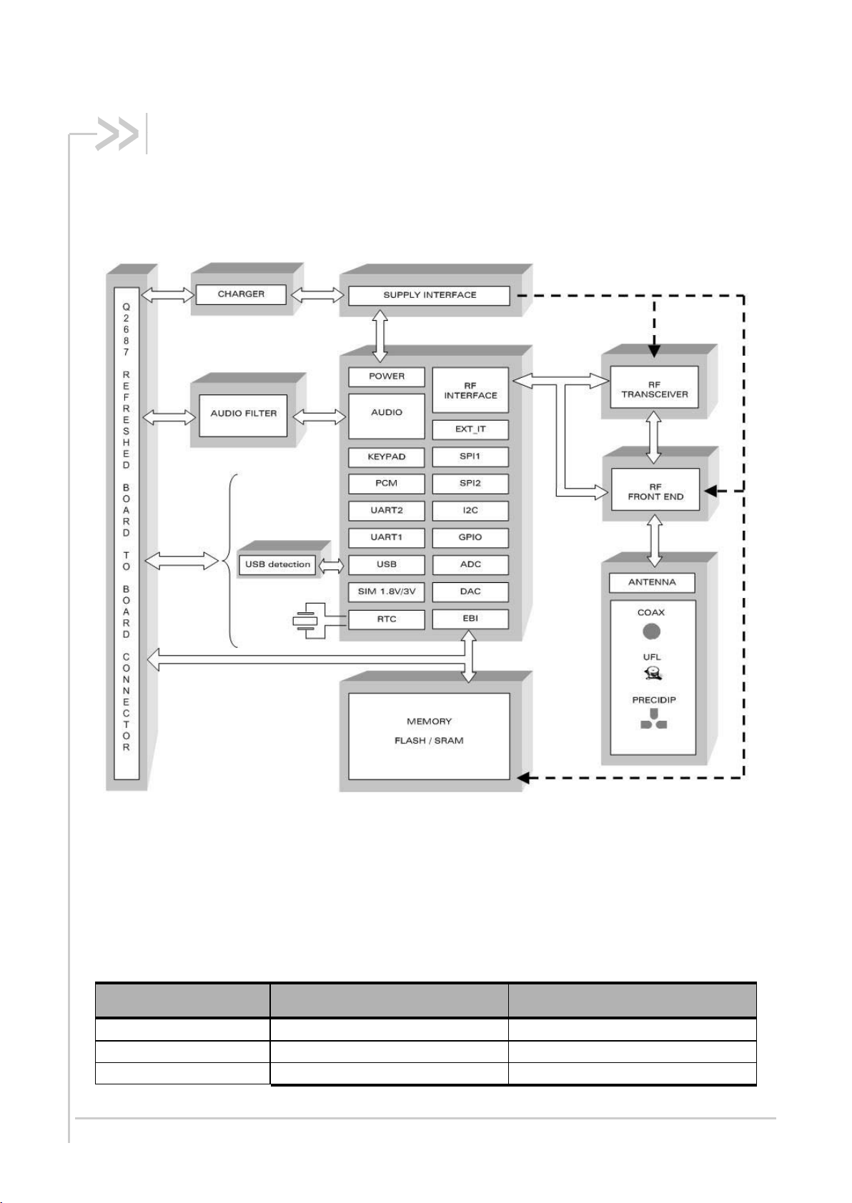
The global architecture of the Q2687 Refreshed Embedded Module is described in the figure below.
Figure 1. Functional Architecture
2.1.1. RF Functionalities
The Radio Frequency (RF) functionalities of the Q2687 Refreshed embedded module complies with
the Phase II EGSM 900/DCS 1800 and GSM 850/PCS 1900 recommendations. The frequency range
for the transmit band and receive band are given in the table below.
Table 2: List of RF Frequency Ranges
WA_DEV_Q26RD_PTS_001 Rev 002 April 20, 2010 20
Page 21

Product Technical Specification and
Customer Design Guideline
Functional Specifications
RF Bandwidth
Transmit Band ( Tx)
Receive Band (Rx)
PCS 1900
1850 to 1910 MHz
1930 to 1990 MHz
The Radio Frequency (RF) component is based on a specific quad-band chip that includes the
following:
Quad-band LNAs (Low Noise Amplifier)
Digital Low-IF Receiver
Offset PLL/PL (Phase Locked Loop and Polar Loop) transmitter
Frequency synthesizer
Digitally controlled crystal oscillator (DCXO)
Tx/Rx FEM (Front-End module) for quad-band GSM/GPRS/EGPRS
2.1.2. Baseband Functionalities
The digital part of the Q2687 Refreshed embedded module is composed of a PCF5213 PHILIPS
chip. This chipset uses a 0.18µm mixed technology CMOS, which allows massive integration as well
as low current consumption.
2.2. Operating System
The Q2687 Refreshed Embedded Module is Sierra Wireless Software Suite compliant. With the Sierra
Wireless Software Suite, customers can embed their own applications with the Q2687 Refreshed
embedded module and turn the Q2687 Refreshed embedded module into a solution for their specific
market need.
The operating system allows for the Q2687 Refreshed Embedded Module to be controlled by AT
commands. However, some interfaces in the Q2687 Refreshed embedded module may still not be
available even with AT command control as these interfaces are dependent on the peripheral devices
connected to the Q2687 Refreshed embedded module.
WA_DEV_Q26RD_PTS_001 Rev 002 April 20, 2010 21
Page 22
3. Technical Specifications
3.1. Power Supply
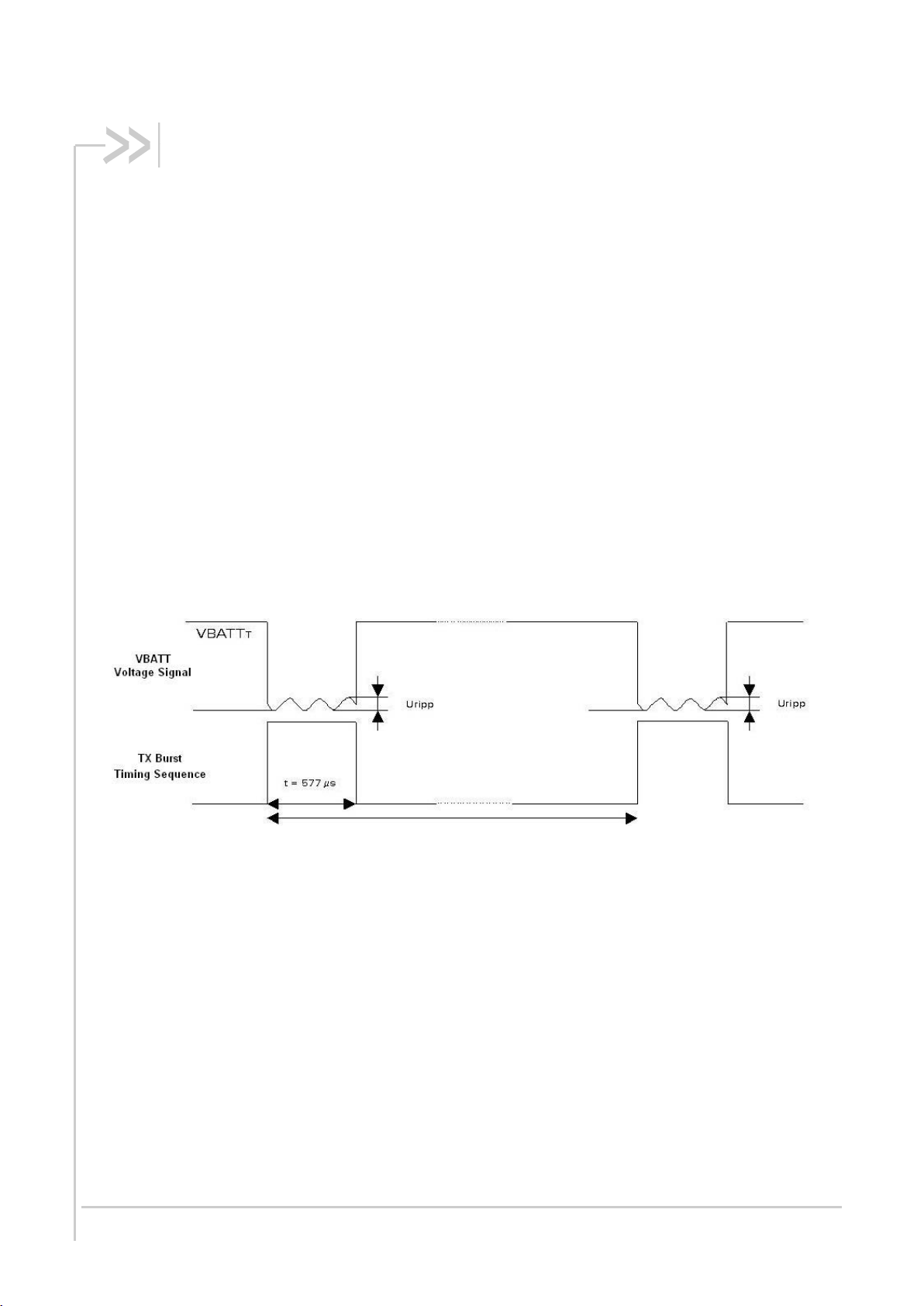
The power supply is one of the key issues in the design of a GSM terminal. Due to the burst emission
in GSM/GPRS, the power supply must be able to deliver high current peaks in a short time. During
these peaks, the ripple (U
Input Power Supply Voltage).
Listed below are the corresponding radio burst rates in connected mode:
GSM/GPRS class 2 terminals emit 577µs radio bursts every 4.615ms (see Figure 2 Power
Supply During Burst Emission)
GPRS class 10 terminals emit 1154µs radio bursts every 4.615ms
In connected mode, the RF Power Amplifier current (2.0A peak in GSM /GPRS mode) flows with a
ratio of:
1/8 of the time (around 577µs every 4.615ms for GSM /GPRS cl 2 – 2RX/1TX)
) on the supply voltage must not exceed a certain limit (refer to Table 3:
ripp
and
2/8 of the time (around 1154µs every 4.615ms for GSM /GPRS cl 10 – 3RX/2TX)
with the rising time at around 10µs.
Figure 2. Power Supply During Burst Emission
Only VBATT (external power supply source) input is necessary to supply the Q2687 Refreshed
embedded module. VBATT also provides for the following functions:
Directly supplies the RF components with 3.6V. (Note that it is essential to keep a minimum
voltage ripple at this connection in order to avoid any phase error or spectrum modulation
degradation. On the other hand, insufficient power supply could dramatically affect some RF
performances such as TX power, modulation spectrum, EMC performance, spurious emission
and frequency error.)
Internally used to provide through several regulators, the power supplies VCC_2V8 and
VCC_1V8, which are needed for the baseband signals.
The Q2687 Refreshed embedded module shielding case is the grounding. The ground must be
connected on the motherboard through a complete layer on the PCB.
The following table describes the electrical characteristics of the input power supply voltage that will
guarantee nominal functioning of the Q2687 Refreshed embedded module.
WA_DEV_Q26RD_PTS_001 Rev 002 April 20, 2010 22
Page 23
Product Technical Specification and
Customer Design Guideline
Technical Specifications
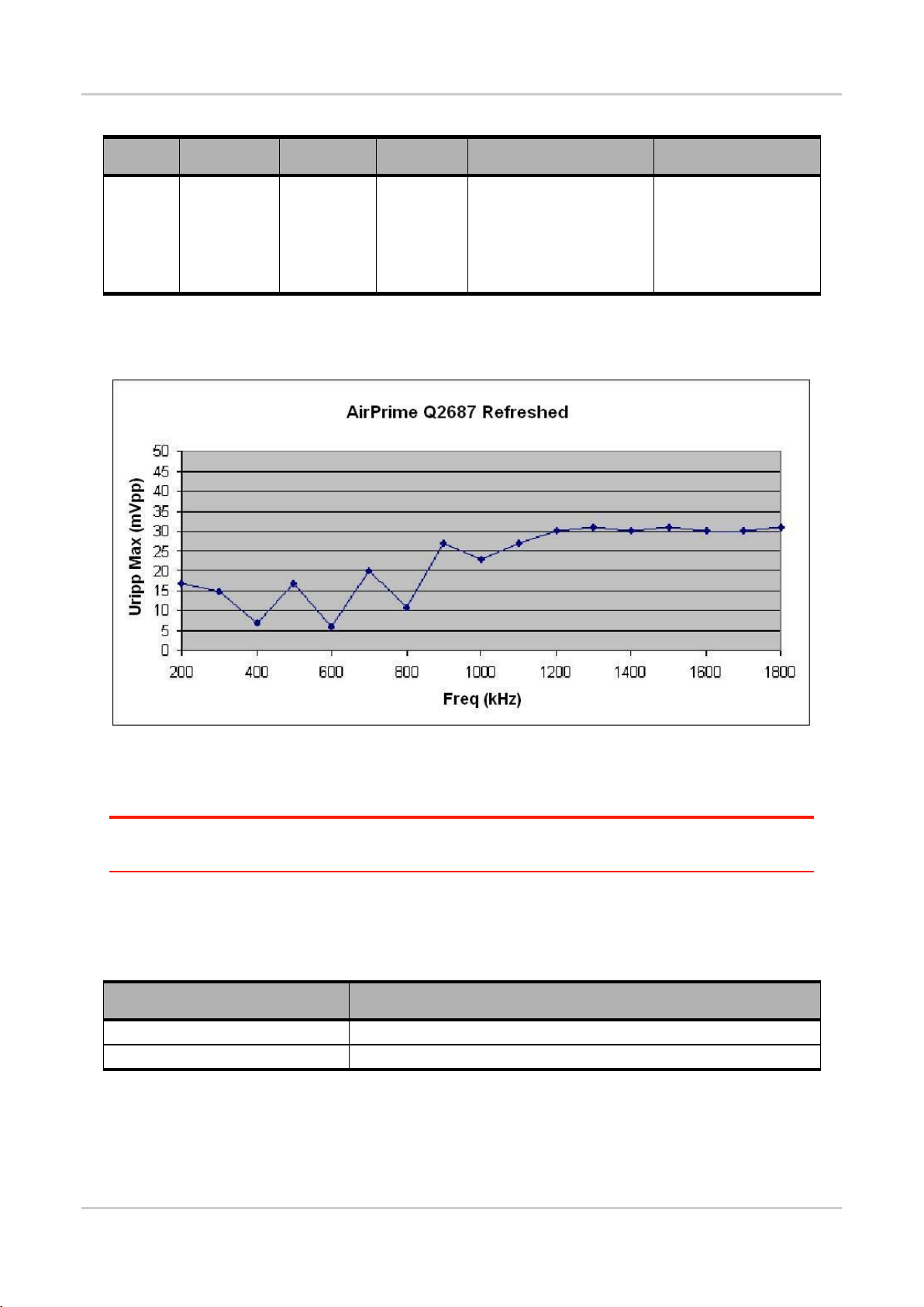
Table 3: Input Power Supply Voltage
V
MI N
V
NO M
V
MA X
Ripple M ax (U
ri pp
)
I
pe ak
M ax
VBATT
3.2V
1,2
3.6V
4.8V
250mVpp (freq < 10kHz)
40mVpp (10kHz < freq <
100kHz)
5mVpp (freq > 100kHz)
(TBC)
2.0A
Signal
Pin Number
VBATT
1, 2, 3, 4
GND
Shielding
1: This value must be guaranteed during the burst (with 2.0A Peak in GSM, GPRS or EGPRS mode)
2: Maximum operating Voltage Standing Wave Ratio (VSW R) 2:1.
Figure 3. Power Supply Ripple Graph (TBC)
When the Q2687 Refreshed embedded module is supplied with a battery, the total impedance
(battery + protections + PCB) should be less than 150 m.
Caution: When the Q2687 Refreshed embedded module is in Alarm mode or Off mode, no voltage has to be
applied on any pin of the 100-pin connector except on VBATT (pins 1 to 4), BAT-RTC (pin 7) for RTC
operation or ON/~OFF (pin 19) to power-ON the Q2687 Refreshed embedded module.
3.1.1. Power Supply Pin-Out
Table 4: Power Supply Pin-Out
The grounding connection is made through the shielding; therefore the four leads must be soldered to
the ground plane.
WA_DEV_Q26RD_PTS_001 Rev 002 April 20, 2010 23
Page 24
Product Technical Specification and
Customer Design Guideline
Technical Specifications
3.1.2. Start-Up Current
Current Pe ak at
Am bien t Temper ature
(25°C)
VBATTmin (3. 2V)
VBATTtyp (3. 6V)
VBATTmax ( 4. 8V)
I
Startup
86 mA
77 mA
64 mA
During the initial second following Power ON, a peak of current appears. This peak of current is called
“I
current” and has a duration of about 161ms (typical) (TBC).
Startup
Figure 4: Start-up Current Waveform shows the current waveform and identifies the peak considered
as the start-up current.
<TBC>
Figure 4. Start-up Current Waveform
In this condition, we can consider the following results:
Table 5: Current Start-Up (TBC)
3.1.3. Decoupling of Power Supply Signals
Decoupling capacitors on VBATT lines are embedded in the Q2687 Refreshed embedded module, so
it should not be necessary to add decoupling capacitors close to the embedded module.
However, in case of EMI/RFI problems, the VBATT signal may require some EMI/RFI decoupling –
parallel 33pF capacitors close to the embedded module or a serial ferrite bead (or both to get better
results). Low frequency decoupling capacitors (22µF to 100µF) can be used to reduce TDMA noise
(217Hz).
Caution: When ferrite beads are used, the recommendation given for the power supply connection must be
carefully followed (high current capacity and low impedance).
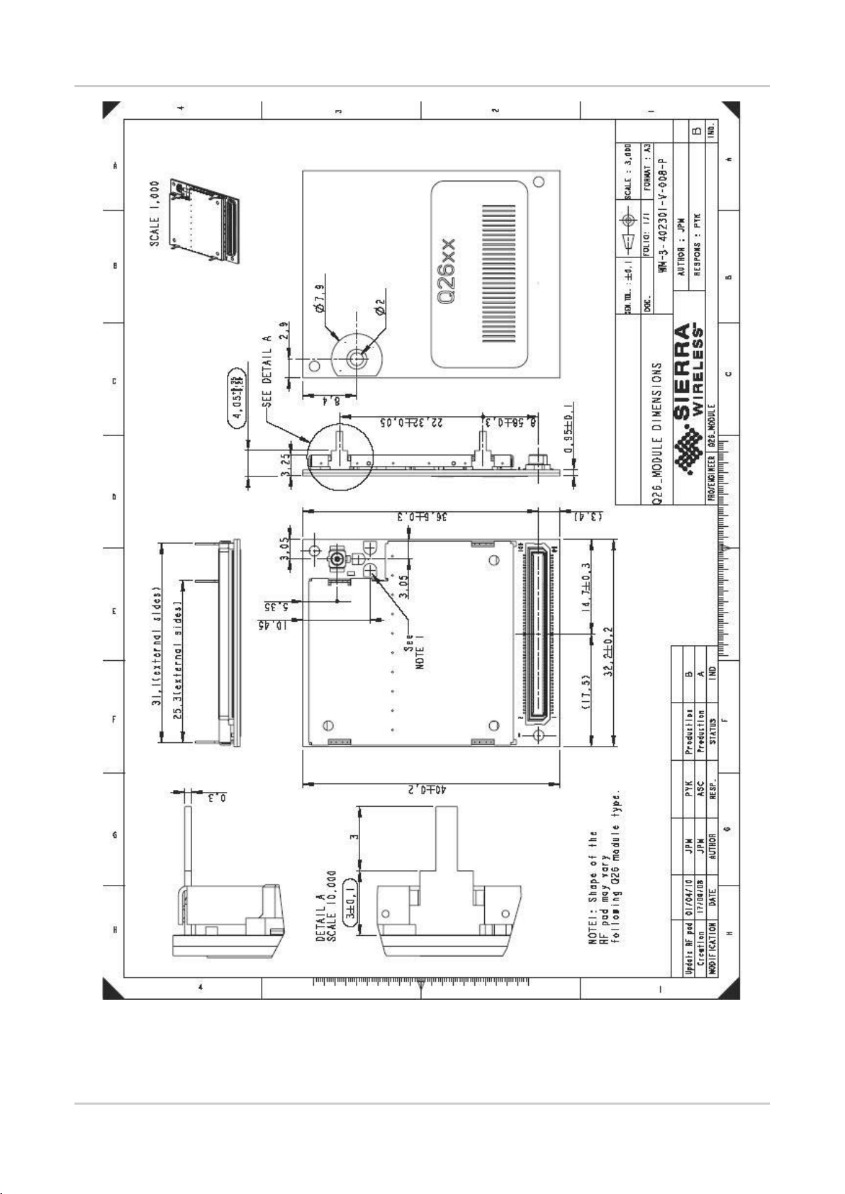
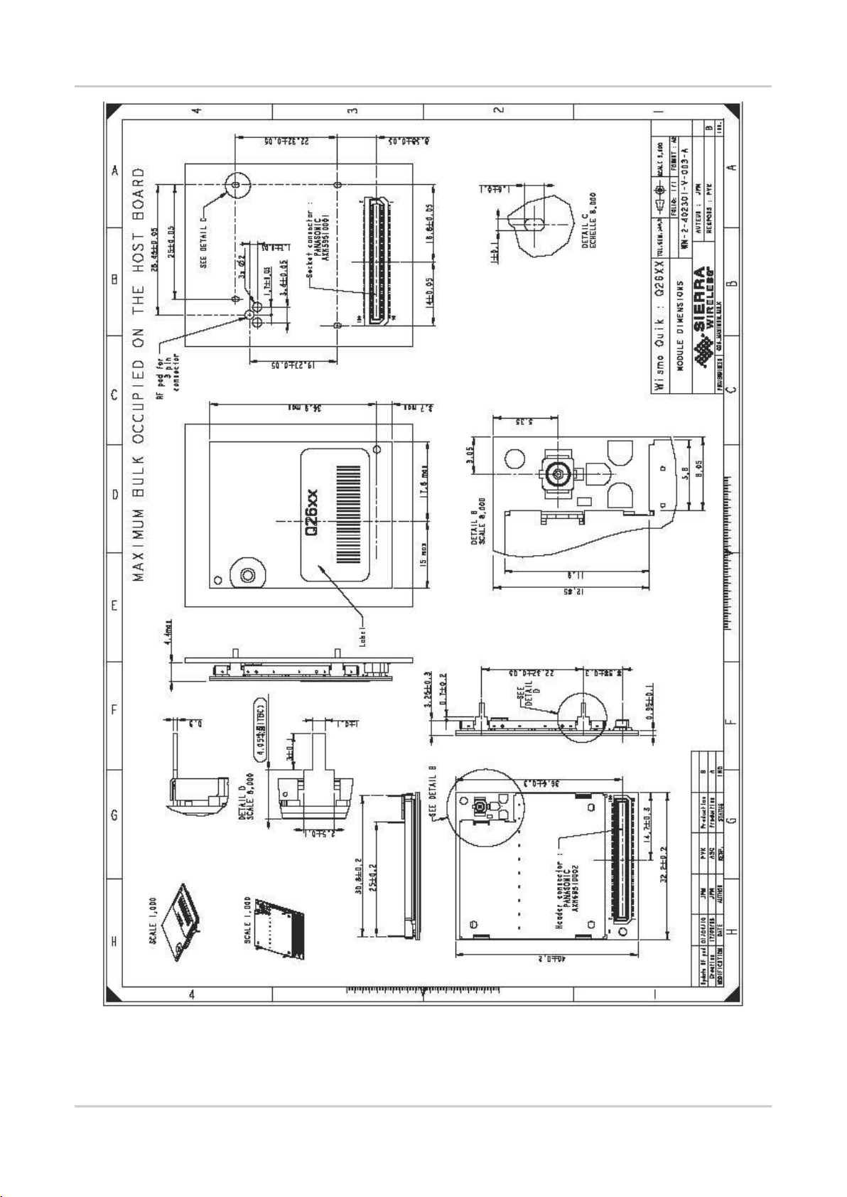
3.2. Mechanical Specifications
The Q2687 Refreshed Embedded Module has a complete self-contained shield and the mechanical
specifications are shown in the figure below, which also specifies the following:
The area needed for the Q2687 Refreshed embedded module to fit in an application
The drill template for the four pads to be soldered on the application board
The dimensions and tolerance for correctly placing the 100-pin female connector on the
application board
It is strongly recommended to plan a free area (no components) around the Q2687 Refreshed
embedded module in order to facilitate the removal/re-assembly of the embedded module on the
application board.
Also take note that when transmitting, the Q2687 Refreshed Embedded Module produces heat (due
to the internal Power Amplifier). This heat will generate a temperature increase and may warm the
application board on which the Q2687 Refreshed embedded module is soldered. This is especially
true for GPRS Class 10 use in low band. The Q2687 Refreshed Embedded Module’s built-in
temperature sensor can be used to monitor the temperature inside the module. For more information,
refer to document [14] AirPrime Q2687 Product Technical Specification.
WA_DEV_Q26RD_PTS_001 Rev 002 April 20, 2010 24
Page 25
Product Technical Specification and
Customer Design Guideline
Technical Specifications
Figure 5. Q2687 Refreshed Embedded Module Mechanical Drawing
WA_DEV_Q26RD_PTS_001 Rev 002 April 20, 2010 25
Page 26
Product Technical Specification and
Customer Design Guideline
Technical Specifications
Figure 6. Maximum Bulk Occupied on the Host Board
WA_DEV_Q26RD_PTS_001 Rev 002 April 20, 2010 26
Page 27

Product Technical Specification and
Customer Design Guideline
Technical Specifications
3.3. Firmware Upgrade
The firmware upgrade process consists of downloading GSM/GPRS/EGPRS software into the
corresponding internal flash memories of the Q2687 Refreshed Intelligent Embedded Module.
Downloading is done through the GSM Main Serial link port (UART1) connected to a PC using the
XMODEM protocol.
A specific AT command, AT+WDWL, is used to start the download. For more information, refer to
document [8] Firmware 7.43 AT Commands Manual (Sierra Wireless Software Suite 2.33).
Access to the following UART1 main serial link signals are required to carry out downloading:
CT103-TXD1
CT104-RXD1
~CT106-CTS1
~CT105-RTS1
GND
Consequently, it is very important to plan and define easy access to these signals during the
hardware design of the application board. For more information about these signals, refer to section
4.7 Main Serial Link (UART1).
WA_DEV_Q26RD_PTS_001 Rev 002 April 20, 2010 27
Page 28
4. Interfaces
Name
Driven by AT commands
Driven by Open AT®
Serial Interface
Parallel Interface
Keyboard Interface
Main Serial Link
Auxiliary Serial Link
SIM Interface
General Purpose IO
Analog to Digital Converter
Analog Audio Interface
PWM / Buzzer Output
Battery Charging Interface
External Interruption
BAT-RTC (Backup Battery)
LED0 signal
Digital Audio Interface (PCM)
USB 2.0 Interface
Caution: Some of the Embedded Module interface signals are multiplexed in order to limit the number of pins
but this architecture includes some restrictions.
4.1. General Purpose Connector (GPC)
A 100-pin connector is provided to interface the Q2687 Refreshed Intelligent Embedded Module with
a board containing either a serial or parallel LCD module; a keyboard, a SIM connector or a battery
connection.
The following table lists the interfaces and signals available on the GPC and specifies whether these
interfaces and signals are driven by AT Command, Open AT® or both.
Table 6: Available Interfaces and Signals
WA_DEV_Q26RD_PTS_001 Rev 002 April 20, 2010 28
Page 29
Product Technical Specification and
Customer Design Guideline
Interfaces
4.1.1. Pin Description
Pin
#
Signal Nam e
I/O
Type
Volt age
I/O*
Reset Stat e
Descri ption
Dealing wi th Unused Pins
Nominal
Mux
1
ADC0/VBATT
VBATT
I Power Supply
2 ADC0/VBATT
VBATT
I Power Supply
3 ADC0/VBATT
VBATT
I Power Supply
4 ADC0/VBATT
VBATT
I Power Supply
5 VCC_1V8
VCC_1V8
O 1.8V Supply Output
NC 6 CHG-IN
CHG-IN
I Charger input
NC
7
BAT-RTC
BAT-RTC
I/O RTC Battery connection
NC
8
CHG-IN
CHG-IN
I Charger input
NC
9
SIM-VCC
1V8 or 3V
O SIM Power Supply
10
VCC_2V8
VCC_2V8
O 2.8V Supply Output
NC
11
SIM-IO
1V8 or 3V
I/O
Pull-up (about
10kΩ)
SIM Data
12
SIMPRES
GPIO18
VCC_1V8
I Z SIM Detection
NC
13
~SIM-RST
1V8 or 3V
O 0 SIM reset Output
14
SIM-CLK
1V8 or 3V
O 0 SIM Clock
15
BUZZER0
Open Drain
O Z Buzzer Output
NC
16
BOOT
VCC_1V8
I Not Used
Add a test point / a jumper/ a switch to
VCC_1V8 (Pin 5) in case Download
Specific mode is used (See product
specification for details)
Refer to the following table for the pin description of the general purpose connector.
Table 7: General Purpose Connector Pin Description
WA_DEV_Q26RD_PTS_001 Rev 002 April 20, 2010 29
Page 30

Product Technical Specification and
Customer Design Guideline
Interfaces
Pin
#
Signal Nam e
I/O
Type
Volt age
I/O*
Reset Stat e
Descri ption
Dealing wi th Unused Pins
Nominal
Mux
17
LED0
Open Drain
O
1 and
Undefined
LED0 Output
NC
18
~RESET
VCC_1V8
I/O RESET Input
NC or add a test point
19
ON/~OFF
VBATT
I ON / ~OFF Control
20
ADC1/BATTEMP
Analog
I Analog temperature
Pull to GND
21
ADC2
Analog
I Analog to Digital Input
Pull to GND
22
GPIO31/ SPI1
Load
VCC_2V8
I/O Z
NC
23
SPI1-CLK
GPIO28
VCC_2V8
O Z SPI1 Clock
NC
24
SPI1-I
GPIO30
VCC_2V8
I Z SPI1 Data Input
NC
25
SPI1-IO
GPIO29
VCC_2V8
I/O Z SPI1 Data Input / Output
NC
26
SPI2-CLK
GPIO32
VCC_2V8
O Z SPI2 Clock
NC
27
SPI2-IO
GPIO33
VCC_2V8
I/O Z SPI2 Data Input / Output
NC
28
GPIO35/SPI2Load
VCC_2V8
I/0 Z
NC
29
SPI2-I
GPIO34
VCC_2V8
I Z SPI2 Data Input
NC
30
CT104-RXD2
GPIO15
VCC_1V8
O Z Auxiliary RS232 Receive
Add a test point for debugging
31
CT103-TXD2
GPIO14
VCC_1V8
I Z Auxiliary RS232 Transmit
(TXD2) Pull-up to VCC_1V8 with 100kΩ
and add a test point for debugging
32
~CT106-CTS2
GPIO16
VCC_1V8
O Z Auxiliary RS232 Clear To Send
(CTS2) Add a test point for debugging
33
~CT105-RTS2
GPIO17
VCC_1V8
I Z Auxiliary RS232 Request To Send
(RTS2) Pull-up to VCC_1V8 with 100kΩ
and add a test point for debugging
34
MIC2N
Analog
I Micro 2 Input Negative
NC
35
SPK1P
Analog
O Speaker 1 Output Positive
NC
36
MIC2P
Analog
I Micro 2 Input Positive
NC
37
SPK1N
Analog
O Speaker 1 Output Negative
NC
38
MIC1N
Analog
I Micro 1 Input Negative
NC
WA_DEV_Q26RD_PTS_001 Rev 002 April 20, 2010 30
Page 31

Product Technical Specification and
Customer Design Guideline
Interfaces
Pin
#
Signal Nam e
I/O
Type
Volt age
I/O*
Reset Stat e
Descri ption
Dealing wi th Unused Pins
Nominal
Mux
39
SPK2P
Analog
O Speaker 2 Output Positive
NC
40
MIC1P
Analog
I Micro 1 Input Positive
NC
41
SPK2N
Analog
O Speaker 2 Output Negative
NC
42
A1
VCC_1V8
O Address bus 1
NC
43
GPIO0
32kHz
VCC_2V8
I/O
32 kHz
NC
44
SCL1
GPIO26
Open Drain
O Z I²C Clock
NC
45
GPIO19
VCC_2V8
I/O Z
NC
46
SDA1
GPIO27
Open Drain
I/O Z I²C Data
NC
47
GPIO21
VCC_2V8
I/O
Undefined
NC
48
GPIO20
VCC_2V8
I/O
Undefined
NC
49
INT1
GPIO25
VCC_2V8
I Z Interruption 1 Input
If INT1 is not used, it should be
configured as GPIO
50
INT0
GPIO3
VCC_1V8
I Z Interruption 0 Input
If INT0 is not used, it should be
configured as GPIO
51
GPIO1
** VCC_1V8
I/O
Undefined
NC
52
VPAD-USB
VPAD-USB
I USB Power supply input
NC
53
GPIO2
** VCC_1V8
I/O
Undefined
NC
54
USB-DP
VPAD-USB
I/O USB Data
NC
55
GPIO23
** VCC_2V8
I/O Z
NC
56
USB-DM
VPAD-USB
I/O USB Data
NC
57
GPIO22
** VCC_2V8
I/O Z
NC
58
GPIO24
VCC_2V8
I/O Z
NC
59
COL0
GPIO4
VCC_1V8
I/O
Pull-up
Keypad column 0
NC
60
COL1
GPIO5
VCC_1V8
I/O
Pull-up
Keypad column 1
NC
61
COL2
GPIO6
VCC_1V8
I/O
Pull-up
Keypad column 2
NC
62
COL3
GPIO7
VCC_1V8
I/O
Pull-up
Keypad column 3
NC
WA_DEV_Q26RD_PTS_001 Rev 002 April 20, 2010 31
Page 32

Product Technical Specification and
Customer Design Guideline
Interfaces
Pin
#
Signal Nam e
I/O
Type
Volt age
I/O*
Reset Stat e
Descri ption
Dealing wi th Unused Pins
Nominal
Mux
63
COL4
GPIO8
VCC_1V8
I/O
Pull-up
Keypad column 4
NC
64
ROW4
GPIO13
VCC_1V8
I/O 0 Keypad Row 4
NC
65
ROW3
GPIO12
VCC_1V8
I/O 0 Keypad Row 3
NC
66
ROW2
GPIO11
VCC_1V8
I/O 0 Keypad Row 2
NC
67
ROW1
GPIO10
VCC_1V8
I/O 0 Keypad Row 1
NC
68
ROW0
GPIO9
VCC_1V8
I/O 0 Keypad Row 0
NC
69
~CT125-RI
GPIO42
VCC_2V8
O
Undefined
Main RS232 Ring Indicator
NC
70
~CT109-DCD1
GPIO43
VCC_2V8
O
Undefined
Main RS232 Data Carrier Detect
NC
71
CT103-TXD1
GPIO36
VCC_2V8
I Z Main RS232 Transmit
(TXD1) Pull-up to VCC_2V8 with 100kΩ
and add a test point for firmware update
72
~CT105-RTS1
GPIO38
VCC_2V8
I Z Main RS232 Request To Send
(RTS1) Pull-up to VCC_2V8 with 100kΩ
and add a test point for firmware update
73
CT104-RXD1
GPIO37
VCC_2V8
O 1 Main RS232 Receive
(RXD1) Add a test point for firmware
update
74
~CT107-DSR1
GPIO40
VCC_2V8
O Z Main RS232 Data Set Ready
NC
75
~CT106-CTS1
GPIO39
VCC_2V8
O Z Main RS232 Clear To Send
(CTS1) Add a test point for firmware
update
76
~CT108-2-DTR1
GPIO41
VCC_2V8
I Z Main RS232 Data Terminal Ready
(DTR1) Pull-up to VCC_2V8 with 100kΩ
77
PCM-SYNC
VCC_1V8
O
Pull-down
PCM Frame Synchro
NC
78
PCM-IN
VCC_1V8
I
Pull-up
PCM Data Input
NC
79
PCM-CLK
VCC_1V8
O
Pull-down
PCM Clock
NC
80
PCM-OUT
VCC_1V8
O
Pull-up
PCM Data Output
NC
81
/OE-R/W
VCC_1V8
O Output Enable/ Read not write
NC
82
DAC0
Analog
O Digital to Analog Output
NC
83
/CS3
VCC_1V8
O Chip Select 3
NC
84
/WE-E
VCC_1V8
O Write Enable
NC
85
D0
VCC_1V8
I/O Data for Peripheral
NC
WA_DEV_Q26RD_PTS_001 Rev 002 April 20, 2010 32
Page 33

Product Technical Specification and
Customer Design Guideline
Interfaces
Pin
#
Signal Nam e
I/O
Type
Volt age
I/O*
Reset Stat e
Descri ption
Dealing wi th Unused Pins
Nominal
Mux
86
D15
VCC_1V8
I/O Data for Peripheral
NC
87
D1
VCC_1V8
I/O Data for Peripheral
NC
88
D14
VCC_1V8
I/O Data for Peripheral
NC
89
D2
VCC_1V8
I/O Data for Peripheral
NC
90
D13
VCC_1V8
I/O Data for Peripheral
NC
91
D3
VCC_1V8
I/O Data for Peripheral
NC
92
D12
VCC_1V8
I/O Data for Peripheral
NC
93
D4
VCC_1V8
I/O Data for Peripheral
NC
94
D11
VCC_1V8
I/O Data for Peripheral
NC
95
D5
VCC_1V8
I/O Data for Peripheral
NC
96
D10
VCC_1V8
I/O Data for Peripheral
NC
97
D6
VCC_1V8
I/O Data for Peripheral
NC
98
D9
VCC_1V8
I/O Data for Peripheral
NC
99
D7
VCC_1V8
I/O Data for Peripheral
NC
100
D8
VCC_1V8
I/O Data for Peripheral
NC
* The I/O direction information is only for the nominal signal. When the signal is configured in GPIO, it can always be an Input or an Output.
** For more information about multiplexing these signals, refer to section 4.3 General Purpose Input/Output.
Refer to section 4.2 Electrical Information for Digital I/O for open drain, 2V8 and 1V8 voltage characteristics and reset state definitions.
WA_DEV_Q26RD_PTS_001 Rev 002 April 20, 2010 33
Page 34

Product Technical Specification and
Customer Design Guideline
Interfaces
4.1.2. Pin Out Differences
Pin #
Q2686
Q2687
Q2687 Refreshed
Signal
Name
Functi on
Value
Signal
Name
Functi on
Value
Signal
Name
Functi on
Value
42
Reserved
Not in Use
-
A1
Address Bus
1V8
A1
Address Bus
1V8
51
GPIO1
General
Purpose IO
1V8
CS2
/A25
/GPIO1
Chip Select,
Address bus,
General
Purpose IO
1V8
CS2
/A25
/GPIO1
Chip Select,
Address bus,
General
Purpose IO
1V8
53
GPIO2
General
Purpose IO
1V8
A24 / GPIO2
Address bus,
General
Purpose IO
1V8
A24 / GPIO2
Address bus,
General
Purpose IO
1V8
83
NC-5
Not Connected
-
/CS3
Chip Select 3
1V8
/CS3
Chip Select 3
1V8
81,
84100
NC
Not Connected
-
Parallel
Interface
Parallel Bus
Interface
1V8
Parallel
Interface
Parallel Bus
Interface
1V8
Although the Q Series Embedded Modules are compatible, one must be careful with regards to their specific signal differences. The following table
enumerates the pin out differences between the Q2686, Q2687 and the Q2687 Refreshed embedded modules.
Table 8: Signal Comparison between the Q Series Intelligent Embedded Modules
WA_DEV_Q26RD_PTS_001 Rev 002 April 20, 2010 34
Page 35

Product Technical Specification and
Customer Design Guideline
Interfaces
4.2. Electrical Information for Digital I/O
Parame ter
I/O Type
Mi nimum
Typical
Maximum
Condit ion
Internal 2.8V power supply
VCC_2V8
2.74V
2.8V
2.86V
Input / Output
Pin
VIL
CMOS
-0.5V*
0.84V
VIH
CMOS
1.96V
3.2V*
VOL
CMOS
0.4V
IOL = - 4 mA
VOH
CMOS
2.4V
IOH = 4 mA
IOH 4mA
IOL - 4mA
Parame ter
I/O Type
Mi nimum
Typical
Maximum
Condit ion
Internal 1.8V power supply
VCC_1V8
1.76V
1.8V
1.94V
Input / Output
Pin
VIL
CMOS
-0.5V*
0.54V
VIH
CMOS
1.33V
2.2V*
VOL
CMOS
0.4V
IOL = - 4 mA
VOH
CMOS
1.4V
IOH = 4 mA
IOH 4mA
IOL - 4mA
Signal Nam e
Parame ter
I/O Type
Mi nimum
Typical
Maximum
Condit ion
LED0
VOL
Open Drain
0.4V
IOL
Open Drain
8mA
BUZZER0
VOL
Open Drain
0.4V
IOL
Open Drain
100mA
SDA1 / GPIO27
and
SCL1 / GPIO26
V
TOL
Open Drain
3.3V
Tolerated voltage
VIH
Open Drain
2V
VIL
Open Drain
0.8V
VOL
Open Drain
0.4V
There are three types of digital I/Os on the Q2687 Refreshed Embedded Module:
2.8 volt CMOS
1.8 volt CMOS
Open drain
Refer to the tables below for the electrical characteristics of these three digital I/Os.
Table 9: Electrical Characteristic of a 2.8 Volt Type (2V8) Digital I/O
* Absolute maximum ratings
All 2.8V I/O pins do not accept input signal voltages above the maximum voltage specified above;
except for the UART1 interface, which is 3.3V tolerant.
Table 10: Electrical Characteristic of a 1.8 Volt Type (1V8) Digital I/O
* Absolute maximum ratings
Table 11: Open Drain Output Type
WA_DEV_Q26RD_PTS_001 Rev 002 April 20, 2010 35
Page 36

Product Technical Specification and
Customer Design Guideline
Interfaces
Signal Nam e
Parame ter
I/O Type
Mi nimum
Typical
Maximum
Condit ion
IOL
Open Drain
3mA
Parame ter
Defi nition
0
Set to GND
1
Set to supply 1V8 or 2V8 depending on I/O type
Pull-down
Internal pull-down with ~60kΩ resistor
Pull-up
Internal pull-up with ~60kΩ resistor to supply 1V8 or 2V8 depending on I/O type
Z
High impedance
Undefined
Caution: Undefined must not be used in an application if a special state is required at
reset. These pins may be toggling a signal(s) during reset.
The reset states of the I/Os are given in each interface description chapter. Definitions of these states
are given in the table below.
Table 12: Reset State Definition
WA_DEV_Q26RD_PTS_001 Rev 002 April 20, 2010 36
Page 37

Product Technical Specification and
Customer Design Guideline
Interfaces
4.3. General Purpose Input/Output
Pin
Number
Signal
I/O
I/O Type
Reset Stat e
Multiplexed With
43
GPIO0
I/O
2V8
Undefined
32kHz***
51
GPIO1
I/O
1V8
Undefined
A25/~CS2*
53
GPIO2
I/O
1V8
Undefined
A24*
50
GPIO3
I/O
1V8 Z INT0
59
GPIO4
I/O
1V8
Pull up
COL0
60
GPIO5
I/O
1V8
Pull up
COL1
61
GPIO6
I/O
1V8
Pull up
COL2
62
GPIO7
I/O
1V8
Pull up
COL3
63
GPIO8
I/O
1V8
Pull up
COL4
68
GPIO9
I/O
1V8 0 ROW0
67
GPIO10
I/O
1V8 0 ROW1
66
GPIO11
I/O
1V8 0 ROW2
65
GPIO12
I/O
1V8 0 ROW3
64
GPIO13
I/O
1V8 0 ROW4
31
GPIO14
I/O
1V8 Z CT103 / TXD2
30
GPIO15
I/O
1V8 Z CT104 / RXD2
32
GPIO16
I/O
1V8 Z ~CT106 / CTS2
33
GPIO17
I/O
1V8 Z ~CT105 / RTS2
12
GPIO18
I/O
1V8 Z SIMPRES
45
GPIO19
I/O
2V8 Z Not mux
48
GPIO20
I/O
2V8
Undefined
Not mux
47
GPIO21
I/O
2V8
Undefined
Not mux
57
GPIO22
I/O
2V8 Z Not mux**
55
GPIO23
I/O
2V8 Z Not mux**
58
GPIO24
I/O
2V8 Z Not mux
49
GPIO25
I/O
2V8 Z INT1
44
GPIO26
I/O
Open drain
Z
SCL1
46
GPIO27
I/O
Open drain
Z
SDA1
23
GPIO28
I/O
2V8 Z SPI1-CLK
25
GPIO29
I/O
2V8 Z SPI1-IO
24
GPIO30
I/O
2V8 Z SPI1-I
22
GPIO31
I/O
2V8 Z
The Q2687 Refreshed Embedded Module provides up to 44 General Purpose I/O. They are used to
control any external device such as a LCD or a Keyboard backlight.
4.3.1. Pin Description
Refer to the following table for the pin description of the general purpose input/output interface.
Table 13: GPIO Pin Description
WA_DEV_Q26RD_PTS_001 Rev 002 April 20, 2010 37
Page 38

Product Technical Specification and
Customer Design Guideline
Interfaces
Pin
Number
Signal
I/O
I/O Type
Reset Stat e
Multiplexed With
26
GPIO32
I/O
2V8 Z SPI2-CLK
27
GPIO33
I/O
2V8 Z SPI2-IO
29
GPIO34
I/O
2V8 Z SPI2-I
28
GPIO35
I/O
2V8 Z
71
GPIO36
I/O
2V8 Z CT103 / TXD1
73
GPIO37
I/O
2V8 1 CT104 / RXD1
72
GPIO38
I/O
2V8 Z ~CT105 / RTS1
75
GPIO39
I/O
2V8 Z ~CT106 / CTS1
74
GPIO40
I/O
2V8 Z ~CT107 / DSR1
76
GPIO41
I/O
2V8 Z ~CT108-2 / DTR1
69
GPIO42
I/O
2V8
Undefined
~CT125 / RI1
70
GPIO43
I/O
2V8
Undefined
~CT109 / DCD1
* If the parallel bus is used, these pins will be mandatory for the parallel bus functionality. Refer to section 4.5
Parallel Interface.
** If a Bluetooth module is used with the Q2687 Refreshed Embedded Module, this GPIO must be reserved.
*** W ith the Sierra Wireless Software Suite 2. For more details, refer to document [8] Firmware 7.43 AT
Commands Manual (Sierra Wireless Software Suite 2.33).
Refer to section 4.2 Electrical Information for Digital I/O for open drain, 2V8 and 1V8 voltage
characteristics and reset state definitions.
WA_DEV_Q26RD_PTS_001 Rev 002 April 20, 2010 38
Page 39

Product Technical Specification and
Customer Design Guideline
Interfaces
4.4. Serial Interface
Oper ation
Maximum
Speed
SPIMode
Duplex
3-wi re Type
4-wi re Type
5-wi re Type
Master
13 Mb/s
0,1,2,3
Half
SPIx-CLK;
SPIx-IO;
GPIOx as CS
SPIx-CLK;
SPIx-IO;
SPIx-I;
GPIOx as CS
SPIx-CLK;
SPIx-IO;
SPIx-I;
GPIOx as CS;
SPIx-LOAD (not muxed
in GPIO)
The Q2687 Refreshed Embedded Module may be connected to an LCD module driver through either
the two SPI buses (3 or 4-wire interface) or through the I2C bus (2-wire interface).
4.4.1. SPI Bus
Both SPI bus interfaces include:
A CLK signal (SPIx-CLK)
An I/O signal (SPIx-IO)
An I signal (SPIx-I)
A CS (Chip Select) signal complying with the standard SPI bus (any GPIO) (~SPIx-CS)
An optional Load signal (only the SPIx-LOAD signal)
4.4.1.1. Characteristics
The following lists the features available on the SPI bus.
Master mode operation
The CS signal must be any GPIO
The LOAD signal (optional) is used for word handling mode (only the SPIx-LOAD signal)
SPI speed is from 102Kbit/s to 13Mbit/s in master mode operation
3 or 4-wire interface (5-wire interface is possible with the optional SPIx-LOAD signal)
SPI-mode configuration: 0 to 3 (for more details, refer to document [8] Firmware 7.43 AT
Commands Manual (Sierra Wireless Software Suite 2.33))
1 to 16 bits data length
4.4.1.2. SPI Configuration
Table 14: SPI Bus Configuration
Refer to section 4.4.1.6 Application for more information on the signals used and their corresponding
configurations.
WA_DEV_Q26RD_PTS_001 Rev 002 April 20, 2010 39
Page 40

Product Technical Specification and
Customer Design Guideline
Interfaces
4.4.1.3. SPI Waveforms
Signal
Descri ption
Mi nimum
Typical
Maximum
Unit
CLK-cycle
SPI clock frequency
0.102
13
MHz
Data-OUT delay
Data out ready delay time
10
ns
Data-IN-setup
Data in setup time
2
ns
Data-OUT-hold
Data out hold time
2
ns
The figure below shows the waveforms for SPI transfers with a 4-wire configuration in master mode 0.
Figure 7. SPI Timing Diagram (Mode 0, Master, 4 wires)
Table 15: SPI Bus AC Characteristics
WA_DEV_Q26RD_PTS_001 Rev 002 April 20, 2010 40
Page 41

Product Technical Specification and
Customer Design Guideline
Interfaces
The following figure shows the waveform for SPI transfer with the LOAD signal configuration in master
Pin
Number
Signal
I/O
I/O Type
Reset
Stat e
Descri ption
Multiplexed With
22
SPI1-LOAD
O
2V8 Z SPI load
GPIO31
23
SPI1-CLK
O
2V8 Z SPI Serial Clock
GPIO28
24
SPI1-I
I
2V8 Z SPI Serial input
GPIO30
25
SPI1-IO
I/O
2V8 Z SPI Serial input/output
GPIO29
Pin
Number
Signal
I/O
I/O Type
Reset
Stat e
Descri ption
Multiplexed With
26
SPI2-CLK
O
2V8 Z SPI Serial Clock
GPIO32
27
SPI2-IO
I/O
2V8 Z SPI Serial input/output
GPIO33
28
SPI2-LOAD
O
2V8 Z SPI load
GPIO35
29
SPI2-I
I
2V8 Z SPI Serial input
GPIO34
mode 0 (chip select is not represented).
Figure 8. SPI Timing Diagram with LOAD Signal (Mode 0, Master, 4 wires)
4.4.1.4. SPI1 Pin Description
Refer to the following table for the SPI1 pin description.
Table 16: SPI1 Pin Description
Refer to section 4.2 Electrical Information for Digital I/O for open drain, 2V8 and 1V8 voltage
characteristics and reset state definitions.
4.4.1.5. SPI2 Pin Description
Refer to the following table for the SPI2 pin description.
Table 17: SPI2 Pin Description
WA_DEV_Q26RD_PTS_001 Rev 002 April 20, 2010 41
Page 42

Product Technical Specification and
Customer Design Guideline
Interfaces
Refer to section 4.2 Electrical Information for Digital I/O for open drain, 2V8 and 1V8 voltage
characteristics and reset state definitions.
4.4.1.6. Application
4.4.1.6.1. 3-wire Application
For the 3-wire configuration, only the SPIx-I/O is used as both input and output.
Figure 9. Example of a 3-wire SPI Bus Application
The SPIx-I line is not used in a 3-wire configuration. Instead, this can be left open or used as a GPIO
for other application functionality.
One pull-up resistor, R1, is needed to set the SPIx-CS level during the reset state. Except for R1, no
other external component is needed is the electrical specifications of the customer application comply
with the Q2687 Refreshed embedded module interface electrical specifications.
Note that the value of R1 depends on the peripheral plugged to the SPIx interface.
4.4.1.6.2. 4-wire Application
For the 4-wire configuration, the input and output data lines are dissociated. SPIx-I/O is used as
output only and SPIx-I is used as input only.
Figure 10. Example of a 4-wire SPI Bus Application
One pull-up resistor, R1, is needed to set the SPIx-CS level during the reset state. Except for R1, no
other external component is needed if the electrical specifications of the customer application comply
with the Q2687 Refreshed embedded module SPIx interface electrical specifications.
WA_DEV_Q26RD_PTS_001 Rev 002 April 20, 2010 42
Page 43

Product Technical Specification and
Customer Design Guideline
Interfaces
4.4.1.6.3. 5-wire Application
Signal
Descri ption
Mi nimum
Typical
Maximum
Unit
SCL1-freq
I²C clock frequency
100 400
kHz
T-start
Hold time START condition
0.6
µs
T-stop
Setup time STOP condition
0.6
µs
T-free
Bus free time, STOP to
START
1.3
µs
T-high
High period for clock
0.6
µs
T-data-hold
Data hold time
0 0.9
µs
T-data-setup
Data setup time
100
ns
For the 5-wire configuration, SPIx-I/O is used as output only and SPIx-I is used as input only. The
dedicated SPIx-LOAD signal is also used. This is an additional signal in more than a Chip Select (any
other GPIOx).
4.4.2. I2C Bus
The I2C Bus interface includes a CLK signal (SCL1) and a data signal (SDA1) complying with a
100kbit/s-standard interface (standard mode: s-mode).
The I2C bus is always in master mode operation.
The maximum speed transfer is 400Kbit/s (fast mode: f-mode).
For more information on the I2C bus, see document [21] “I2C Bus Specification”, Version 2.0, Philips
Semiconductor 1998.
4.4.2.1. I2C Waveforms
The figure below shows the I2C bus waveform in master mode configuration.
Figure 11. I2C Timing Diagram (master)
Table 18: I2C AC Characteristics
WA_DEV_Q26RD_PTS_001 Rev 002 April 20, 2010 43
Page 44

Product Technical Specification and
Customer Design Guideline
Interfaces
4.4.2.2. I2C Pin Description
Pin
Number
Signal
I/O
I/O Type
Reset
Stat e
Descri ption
Multiplexed With
44
SCL1
O
Open drain
Z
Serial Clock
GPIO26
46
SDA1
I/O
Open drain
Z
Serial Data
GPIO27
Refer to the following table for the I2C pin description.
Table 19: I2C Pin Description
Refer to section 4.2 Electrical Information for Digital I/O for open drain, 2V8 and 1V8 voltage
characteristics and reset state definitions.
4.4.2.3. Application
Figure 12. Example1 of an I2C Bus Application
The two lines, SCL1 and SDA1, both need to be pulled-up to the VI
2
C voltage. Although the VI2C
voltage is dependent on the customer application component connected to the I2C bus, it must comply
with the Q2687 Refreshed embedded module electrical specifications.
The VCC_2V8 (pin 10) of the Q2687 Refreshed embedded module can be used to connect the pullup resistors if the I2C bus voltage is 2.8V.
Figure 13. Example2 of an I2C Bus Application
The I2C bus complies with both the standard mode (baud rate = 100Kbit/s) and the fast mode (baud
rate = 400Kbit/s). The value of the pull up resistors varies depending on the mode used. When using
Fast mode, it is recommended to use 1KΩ resistors to ensure compliance with the I2C specifications.
When using Standard mode, a higher resistance value can be used to save power consumption.
WA_DEV_Q26RD_PTS_001 Rev 002 April 20, 2010 44
Page 45

Product Technical Specification and
Customer Design Guideline
Interfaces
4.5. Parallel Interface
3CS
WE
OE
/RW
Pin
Number
Signal
I/O
I/O
Type
Reset
Stat e
Descri ption
Multiplexed
With
42
A1 O 1V8
1
This signal has 2 functions: external
Address or byte enable 2 for 16 or 32
bits devices.
Another name is used: A1_BE2
Not mux
51
/CS2
I/O
1V8
Undefined
User Chip Select 2
A25/GPIO1
53
A24
I/O
1V8
Undefined
Address line for external
device/Command selection
GPIO2
81
/OE-R/W
O
1V8
1
Output enable signal (Intel mode);
read not write signal (Motorola mode)
Not mux
The Q2687 Refreshed Intelligent Embedded Module may be connected to a NAND memory through
the 16-bit 1.8V parallel bus interface. The VCC_1V8 (pin 5) of the Q2687 Refreshed embedded
module can be used to supply the power to this interface.
The following lists the features available on the parallel interface.
Up to 128MB address range per chip select (CSand
)
Support for 8, 16, and 32 bit (multiplexed synchronous mode) devices
Byte enabled signals for 16 bit and 32 bit operations
Fully programmable timings based on AHB (a division of the ARM clock at 26 MHz ) cycles
(except for synchronous mode which is based on CLKBURST cycles at 26 MHz only):
individually selectable timings for read and write
0 to 7 clock cycles for setup
1 to 32 clock cycles for access cycle
1 to 8 clock cycles for page access cycle
0 to 7 clock cycles for hold
1 to 15 clock cycles for turnaround
Page mode Flash memory support
page size of 4, 8, 16 or 32
Burst mode Flash memory support up to AHB (26 MHz) clock frequency (for devices sensitive
to rising edge of the clock only)
AHB, AHB/2, AHB/4 or AHB/8 burst clock output
burst size of 4, 8, 16, 32
automatic CLKBURST power-down between accesses
Intel mode (
and
) and Motorola mode (E and
) control signals
Synchronous write mode
Synchronous multiplexed data/address mode (x32 mode)
Adaptation to word, half word, and byte accesses to the external devices
4.5.1. Pin Description
Refer to the following table for the pin description of the Parallel Interface.
Table 20: Parallel Interface Pin Description
WA_DEV_Q26RD_PTS_001 Rev 002 April 20, 2010 45
Page 46

Product Technical Specification and
Customer Design Guideline
Interfaces
Pin
Number
Signal
I/O
I/O
Type
Reset
Stat e
Descri ption
Multiplexed
With
83
/CS3
O
1V8 1 User Chip select 3
Not mux
84
/WE-E
O
1V8
1
Write enable Signal (Intel mode)
enable signal (Motorola mode)
Not mux
85
D0
I/O
1V8
Pull down
Bidirectional data and address line
Not mux
86
D15
I/O
1V8
Pull down
Bidirectional data and address line
Not mux
87
D1
I/O
1V8
Pull down
Bidirectional data and address line
Not mux
88
D14
I/O
1V8
Pull down
Bidirectional data and address line
Not mux
89
D2
I/O
1V8
Pull down
Bidirectional data and address line
Not mux
90
D13
I/O
1V8
Pull down
Bidirectional data and address line
Not mux
91
D3
I/O
1V8
Pull down
Bidirectional data and address line
Not mux
92
D12
I/O
1V8
Pull down
Bidirectional data and address line
Not mux
93
D4
I/O
1V8
Pull down
Bidirectional data and address line
Not mux
94
D11
I/O
1V8
Pull down
Bidirectional data and address line
Not mux
95
D5
I/O
1V8
Pull down
Bidirectional data and address line
Not mux
96
D10
I/O
1V8
Pull down
Bidirectional data and address line
Not mux
97
D6
I/O
1V8
Pull down
Bidirectional data and address line
Not mux
98
D9
I/O
1V8
Pull down
Bidirectional data and address line
Not mux
99
D7
I/O
1V8
Pull down
Bidirectional data and address line
Not mux
100
D8
I/O
1V8
Pull down
Bidirectional data and address line
Not mux
CS
2CS
3CS
BE
2BE
OE
OE_/RW
WE
WE
ADV
Refer to section 4.2 Electrical Information for Digital I/O for open drain, 2V8 and 1V8 voltage
characteristics and reset state definitions.
4.5.2. Electrical Characteristics
4.5.3. Asynchronous Access
For all timing diagrams in the following section, the notations hereafter are used:
ADR is used for address bus A24, A1 or D[15:0] when used as address lines
DATA is used for D[15:0] when used as DATA lines
is used for
is used for A1_
and R/W are used for
and E are used for
or
(Double function on A1 pin)
_E
signal (not available on 100-pin connector) is the address valid signal
WA_DEV_Q26RD_PTS_001 Rev 002 April 20, 2010 46
Page 47

Product Technical Specification and
Customer Design Guideline
Interfaces
ADV
Signal
Descri ption
Mi nimum
Typical
Maximum
Unit
T
ADR_DELAY
ADR delay time from
CS
active
3
ns
T
DATA_SETUP
DATA to OE setup time
18
ns
T
DATA_HOLD
DATA hold time after OE
inactive
3 4
ns
T
DATA_DELAY
DATA delay time from CS
active
5
ns
T
DATA_SECURE
DATA hold time after
WE
inactive or CS inactive
-5
[1]
ns
T
ADV_DELAY
ADV delay time from
CS
active and inactive
3
ns
T
WE_DELAY
WE
delay time from CS
active
3
[2]
ns
Figure 14. Asynchronous Access
The
signal is mentioned here because synchronous mode devices may require the signal to
be asserted when an asynchronous access is performed.
Refer to the table below for the AC characteristics of asynchronous accesses.
Table 21: AC Characteristics of Asynchronous Accesses
WA_DEV_Q26RD_PTS_001 Rev 002 April 20, 2010 47
Page 48

Product Technical Specification and
Customer Design Guideline
Interfaces
Signal
Descri ption
Mi nimum
Typical
Maximum
Unit
T
OE_DELAY
OE
delay time from CS
active
3
[2]
ns
T
BE_DELAY
BE
delay time from CS
active
3
ns
[1] This timing forces to program at least one cycle for asynchronous
CS
2CS
3CS
BE
2BE
OE
OE_/RW
WE
WE
ADV
BAA
WAIT
[2] These maximum delays also depends on the setting of registers
4.5.4. Synchronous Access
For all timing diagrams in the following section, the notations hereafter are used:
ADR is used for address bus as A24, A1 or D[15:0] when used as address lines
DATA is used for D[15:0] when used as data lines
is used for
or
is used for A1_
and R/W are used for
and E are used for
(Double function on A1 pin)
_E
CLKBURST is the internal clock at 26MHz (not available on connector pin-out)
signal (not available on 100-pin connector) is the address valid signal
signal (not available on 100-pin connector) is the burst address advance for
synchronous operations
signal (not available on 100-pin connector) is the wait signal for synchronous
operation
WA_DEV_Q26RD_PTS_001 Rev 002 April 20, 2010 48
Page 49

Product Technical Specification and
Customer Design Guideline
Interfaces
Figure 15. Synchronous Access
Figure 16. Read Synchronous Timing
WA_DEV_Q26RD_PTS_001 Rev 002 April 20, 2010 49
Page 50

Product Technical Specification and
Customer Design Guideline
Interfaces
Signal
Descri ption
Mi nimum
Typical
Maximum
Unit
T
DATA_DELAY
CLKBURTS falling edge to
DATA valid delay
4
ns
T
WE_SETUP
WE
to CLKBURST setup
time
7
ns
T
BE_DELAY
CLKBURST falling edge to
BE
delay
4
ns
T
CLKBURST
CLKBURST clock : period
time
38.4
ns
T
ADR_SETUP
Address bus setup time
7
ns
T
ADR_HOLD
Address bus hold time
19
ns
T
ADR_TRISTATE
Address bus tristate time
10
ns
T
DATA_SETUP
Data bus setup time
5
ns
T
DATA_HOLD
Data bus hold time
3
ns
T
CS_SETUP
Chip select setup time
7
ns
T
ADV_SETUP
ADV
setup time
7
ns
T
ADV_HOLD
ADV
hold time
7
ns
T
OE_DELAY
Output Enable delay time
13
T
BAA_DELAY
BAA
delay time
13
ns
T
WAIT_SETUP
Wait setup time
5
ns
Figure 17. Write Synchronous Timing
Refer to the table below for the AC characteristics of the synchronous accesses.
Table 22: AC Characteristics of Synchronous Accesses
WA_DEV_Q26RD_PTS_001 Rev 002 April 20, 2010 50
Page 51

Product Technical Specification and
Customer Design Guideline
Interfaces
Signal
Descri ption
Mi nimum
Typical
Maximum
Unit
T
WAIT_HOLD
Wait hold time
5
ns
4.5.5. Additional Information Regarding Address Size
Address Bu s Si ze
Address Lines
Chip Select Available
Notes
1
A1
/CS2, /CS3
2 A1, A24
/CS2, /CS3
3 A1, A24, A25
/CS3
A25 is multiplexed with /CS2
Bus
The following table establishes the possible configurations depending on address bus size requested
on parallel interface.
Table 23: Address Bus Size Details
Note that some signals are multiplexed. It is thus possible to have the following configurations:
CS3*, A1, GPIO1, GPIO2
CS3*, A1, A24, GPIO1
CS3*, A1, A24, A25;
CS3*, CS2*, A1, GPIO2
CS3*, CS2*, A1, A24
4.5.6. Application
Figure 18. Example of a Parallel Bus Application (NAND Memory)
When interfaced with a NAND memory, VCC_1V8 (pin 5) can be used to supply the power to the
NAND.
WA_DEV_Q26RD_PTS_001 Rev 002 April 20, 2010 51
Page 52

Product Technical Specification and
Customer Design Guideline
Interfaces
4.6. Keyboard Interface
Pin
Number
Signal
I/O
I/O Type
Reset
Stat e
Descri ption
Multiplexed With
59
COL0
I/O
1V8
Pull-up
Column scan
GPIO4
60
COL1
I/O
1V8
Pull-up
Column scan
GPIO5
61
COL2
I/O
1V8
Pull-up
Column scan
GPIO6
62
COL3
I/O
1V8
Pull-up
Column scan
GPIO7
63
COL4
I/O
1V8
Pull-up
Column scan
GPIO8
64
ROW4
I/O
1V8 0 Row scan
GPIO13
65
ROW3
I/O
1V8 0 Row scan
GPIO12
66
ROW2
I/O
1V8 0 Row scan
GPIO11
67
ROW1
I/O
1V8 0 Row scan
GPIO10
68
ROW0
I/O
1V8 0 Row scan
GPIO9
This interface provides 10 connections:
5 rows (ROW0 to ROW4)
and
5 columns (COL0 to COL4)
Scanning is digital and debouncing is performed in the Q2687 Refreshed Embedded Module. No
discreet components like resistors or capacitors are needed when using this interface.
The keyboard scanner is equipped with the following:
Internal pull-down resistors for the rows
Pull-up resistors for the columns
Note that current only flows from the column pins to the row pins. This allows transistors to be used in
place of the switch for power-on functions.
4.6.1. Pin Description
Refer to the following table for the pin description of the keyboard interface.
Table 24: Keyboard Interface Pin Description
Refer to section 4.2 Electrical Information for Digital I/O for open drain, 2V8 and 1V8 voltage
characteristics and reset state definitions.
With the Sierra Wireless Software Suite 2, when the keyboard service is used, the set of multiplexed
signals becomes unavailable for any other purpose. In the same way, if one or more GPIOs (from the
table above) are allocated elsewhere, the keyboard service becomes unavailable.
WA_DEV_Q26RD_PTS_001 Rev 002 April 20, 2010 52
Page 53

Product Technical Specification and
Customer Design Guideline
Interfaces
4.6.2. Application
Figure 19. Example of a Keyboard Implementation
WA_DEV_Q26RD_PTS_001 Rev 002 April 20, 2010 53
Page 54

Product Technical Specification and
Customer Design Guideline
Interfaces
4.7. Main Serial Link (UART1)
Pin
Number
Signal *
I/O
I/O Type
Reset
Stat e
Descri ption
Multiplexed
With
69
~CT125/RI1
O
2V8
Undefined
Ring Indicator
GPIO42
70
~CT109/DCD1
O
2V8
Undefined
Data Carrier Detect
GPIO43
71
CT103/TXD1
I
2V8 Z Transmit serial data
GPIO36
72
~CT105/RTS1
I
2V8 Z Request To Send
GPIO38
73
CT104/RXD1
O
2V8 1 Receive serial data
GPIO37
74
~CT107/DSR1
O
2V8 Z Data Set Ready
GPIO40
75
~CT106/CTS1
O
2V8 Z Clear To Send
GPIO39
76
~CT108-2/DTR1
I
2V8 Z Data Terminal Ready
GPIO41
Shielding
leads
CT102/GND
GND
Ground
The main serial link (UART1) is used for communication between the Q2687 Refreshed embedded
module and a PC or host processor. It consists of a flexible 8-wire serial interface that complies with
V24 protocol signalling, but not with the V28 (electrical interface) due to its 2.8V interface.
To get a V24/V28 (i.e. RS-232) interface, an RS-232 level shifter device is required as described in
section 4.7.2 Level Shifter Implementation.
The signals used by UART1 are as follows:
TX data (CT103/TXD1)
RX data (CT104/RXD1)
Request To Send (~CT105/RTS1)
Clear To Send (~CT106/CTS1)
Data Terminal Ready (~CT108-2/DTR1)
Data Set Ready (~CT107/DSR1)
Data Carrier Detect (~CT109/DCD1)
Ring Indicator (CT125/RI1)
4.7.1. Pin Description
Refer to the following table for the pin description of the UART1 interface.
Table 25: UART1 Pin Description
* According to PC view
Refer to section 4.2 Electrical Information for Digital I/O for open drain, 2V8 and 1V8 voltage
characteristics and reset state definitions.
With the Sierra Wireless Software Suite 2, when the UART1 service is used, the set of multiplexed
signals becomes unavailable for any other purpose. In the same way, if one or more GPIOs (from the
table above) are allocated elsewhere, the UART1 service becomes unavailable.
The maximum baud rate of UART1 is 921kbit/s with the Sierra Wireless Software Suite 2.33.
The rise and fall times of the reception signals (mainly CT103/TXD1) must be less than 300ns.
The UART1 interface is 2.8V type, but it is 3V tolerant.
WA_DEV_Q26RD_PTS_001 Rev 002 April 20, 2010 54
Page 55

Product Technical Specification and
Customer Design Guideline
Interfaces
Tip: The Q2687 Refreshed embedded module is designed to operate using all the serial interface signals
and it is recommended to use ~CT105/RTS1 and ~CT106/CTS1 for hardware flow control in order to
avoid data corruption or loss during transmissions.
4.7.2. Level Shifter Implementation
The level shifter must be a 2.8V with V28 electrical signal compliance.
Figure 20. Example of an RS-232 Level Shifter Implementation for UART1
Note: The U1 chip also protects the Q2687 Refreshed embedded module against ESD at 15KV (air
discharge).
4.7.2.1. Recommended Components
R1, R2 :15KΩ
C1, C2, C3, C4, C5 :1uF
C6 :100nF
C7 :6.8uF TANTAL 10V CP32136 AVX
U1 :ADM3307EACP ANALOG DEVICES
J1 :SUB-D9 female
R1 and R2 are only necessary during the Reset state to force the ~CT1125-RI1 and ~CT109-DCD1
signals to HIGH level.
The ADM3307EACP chip is able to speed up to 921Kb/s. If others level shifters are used, ensure that
their speeds are compliant with the UART1 speed.
The ADM3307EACP can be powered by the VCC_2V8 (pin 10) of the Q2687 Refreshed embedded
module or by an external regulator at 2.8 V.
If the UART1 interface is connected directly to a host processor, it is not necessary to use level
shifters. The interface can be connected as defined in the following sub-section.
WA_DEV_Q26RD_PTS_001 Rev 002 April 20, 2010 55
Page 56

Product Technical Specification and
Customer Design Guideline
Interfaces
4.7.3. V24/CMOS Possible Designs
Figure 21. Example of V24/CMOS Serial Link Implementation for UART1
Note that the design presented above is a basic one and that a more flexible design to access the
serial link with all modem signals is presented below.
Figure 22. Example of a Full Modem V24/CMOS Serial Link Implementation for UART1
It is recommended to add a 15kΩ pull-up resistor on the ~CT125-RI1 and ~CT109-DCD1 signals to
set them to HIGH level during the reset state.
Caution: In case the Power Down mode (Wavecom 32K mode) is to be activated using the Sierra Wireless
Software Suite, the DTR pin must be wired to a GPIO. Refer to document [8] Firmware 7.43 AT
Commands Manual (Sierra Wireless Software Suite 2.33) for more information regarding using the
Sierra Wireless Software Suite to activate Wavecom 32K mode.
WA_DEV_Q26RD_PTS_001 Rev 002 April 20, 2010 56
Page 57

Product Technical Specification and
Customer Design Guideline
Interfaces
4.7.4. 5-wire Serial Interface
The signals used in this interface are as follows:
CT103/TXD1
CT104/RXD1
~CT105/RTS1
~CT106/CTS1
~CT108-2/DTR1
The signal ~CT108-2/DTR1* must be managed following the V24 protocol signaling if slow (or fast)
idle mode is to be used.
The other signals and their multiplexed GPIOs are not available.
Refer to the technical appendixes of document [8] Firmware 7.43 AT Commands Manual (Sierra
Wireless Software Suite 2.33) for more information.
4.7.5. 4-wire Serial Interface
The signals used in this interface are as follows:
CT103/TXD1
CT104/RXD1
~CT105/RTS1
~CT106/CTS1
The signal ~CT108-2/DTR1* must be configured from low level.
The other signals and their multiplexed GPIOs are not available.
Refer to the technical appendixes of document [8] Firmware 7.43 AT Commands Manual (Sierra
Wireless Software Suite 2.33) for more information.
4.7.6. 2-wire Serial Interface
Caution: Although this case is possible for a connected external chip, it is not recommended (and forbidden for
AT command or modem use).
The flow control mechanism has to be managed from the customer side. The signals used in this
interface are as follows:
CT103/TXD1
CT104/RXD1
Signals ~CT108-2/DTR1 and ~CT105/RTS1 must be configured from low level.
Signals ~CT105/RTS1 and ~CT106/CTS1 are not used; default hardware flow control on UART1
should be de-activated using AT command AT+IFC=0,0. Refer to document [8] Firmware 7.43 AT
Commands Manual (Sierra Wireless Software Suite 2.33).
The other signals and their multiplexed GPIOs are not available.
Refer to the technical appendixes of document [8] Firmware 7.43 AT Commands Manual (Sierra
Wireless Software Suite 2.33) for more information.
WA_DEV_Q26RD_PTS_001 Rev 002 April 20, 2010 57
Page 58

Product Technical Specification and
Customer Design Guideline
Interfaces
4.8. Auxiliary Serial Link (UART2)
Pin
Number
Signal *
I/O
I/O Type
Reset
Stat e
Descri ption
Multiplexed With
30
CT104/RXD2
O
1V8 Z Receive serial data
GPIO15
31
CT103/TXD2
I
1V8 Z Transmit serial data
GPIO14
32
~CT106/CTS2
O
1V8 Z Clear To Send
GPIO16
33
~CT105/RTS2
I
1V8 Z Request To Send
GPIO17
The auxiliary serial link (UART2) is used for communications between the Q2687 Refreshed
embedded module and external devices. It consists of a flexible 4-wire serial interface that complies
with V24 protocol signaling, but not with the V28 (electrical interface) due to its 1.8V interface.
To get a V24/V28 (i.e. RS-232) interface, an RS-232 level shifter device is required as described in
section 4.8.2 Level Shifter Implementation.
Refer to documents [20] Bluetooth Interface Application Note and [8] Firmware 7.43 AT Commands
Manual (Sierra Wireless Software Suite 2.33) for more information about the Bluetooth application on
the auxiliary serial interface (UART2).
The signals used by UART1 are as follows:
TX data (CT103/TXD2)
RX data (CT104/RXD2)
Request To Send (~CT105/RTS2)
Clear To Send (~CT106/CTS2)
4.8.1. Pin Description
Refer to the following table for the pin description of the UART2 interface.
Table 26: UART2 Pin Description
* According to PC view
Refer to section 4.2 Electrical Information for Digital I/O for open drain, 2V8 and 1V8 voltage
characteristics and reset state definitions.
The maximum baud rate of UART2 is 921kbit/s with the Sierra Wireless Software Suite 2.33.
Tip: The Q2687 Refreshed embedded module is designed to operate using all the serial interface signals
and it is recommended to use ~CT105/RTS2 and ~CT106/CTS2 for hardware flow control in order to
avoid data corruption during transmissions.
WA_DEV_Q26RD_PTS_001 Rev 002 April 20, 2010 58
Page 59

Product Technical Specification and
Customer Design Guideline
Interfaces
4.8.2. Level Shifter Implementation
The voltage level shifter must be a 1.8V with V28 electrical signal compliance.
Figure 23. Example of RS-232 Level Shifter Implementation for UART2
4.8.2.1. Recommended Components
Capacitors
C1 :220nF
C2, C3, C4 :1µF
Inductor
L1 :10µH
RS-232 Transceiver
U1 :LINEAR TECHNOLOGY LTC® 2804IGN
J1 :SUB-D9 female
The LTC2804 can be powered by the VCC_1V8 (pin 5) of the Q2687 Refreshed embedded module or
by an external regulator at 1.8 V.
The UART2 interface can be connected directly to others components if the voltage interface is 1.8V.
WA_DEV_Q26RD_PTS_001 Rev 002 April 20, 2010 59
Page 60

Product Technical Specification and
Customer Design Guideline
Interfaces
4.8.3. 4-wire Serial Interface
The signals used in this interface are as follows:
CT103/TXD2
CT104/RXD2
~CT105/RTS2
~CT106/CTS2
The other signals and their multiplexed GPIOs are not available.
Refer to the technical appendixes of document [8] Firmware 7.43 AT Commands Manual (Sierra
Wireless Software Suite 2.33) for more information.
4.8.4. 2-wire Serial Interface
Caution: Although this case is possible for a connected external chip, it is not recommended (and forbidden for
AT command or modem use).
The flow control mechanism has to be managed from the customer side. The signals used in this
interface are as follows:
CT103/TXD2
CT104/RXD2
Signals ~CT105/RTS2 and ~CT106/CTS2 are not used; default hardware flow control on UART2
should be de-activated using AT command AT+IFC=0,0. Refer to document [8] Firmware 7.43 AT
Commands Manual (Sierra Wireless Software Suite 2.33).
The signal ~CT105/RTS2* must be configured from low level.
The other signals and their multiplexed GPIOs are not available.
Refer to the technical appendixes of document [8] Firmware 7.43 AT Commands Manual (Sierra
Wireless Software Suite 2.33) for more information.
WA_DEV_Q26RD_PTS_001 Rev 002 April 20, 2010 60
Page 61

Product Technical Specification and
Customer Design Guideline
Interfaces
4.9. SIM Interface
Pin
Number
Signal
I/O
I/O Type
Reset
Stat e
Descri ption
Multiplexed With
9
SIM-VCC
O
2V9 / 1V8
SIM Power Supply
Not mux
11
SIM-IO
I/O
2V9 / 1V8
*Pull-up
SIM Data
Not mux
12
SIMPRES
I
1V8 Z SIM Card Detect
GPIO18
13
~SIM-RST
O
2V9 / 1V8
0
SIM Reset
Not mux
14
SIM-CLK
O
2V9 / 1V8
0
SIM Clock
Not mux
Parame ter
Condit ions
Mi nimum
Typical
Maximum
Unit
SIM-IO VIH
IIH = ± 20µA
0.7xSIMVCC
V
SIM-IO VIL
IIL = 1mA
0.4
V
~SIM-RST, SIM-CLK
VOH
Source current = 20µA
0.9xSIMVCC
V
SIM-IO VOH
Source current = 20µA
0.8xSIMVCC
~SIM-RST, SIM-IO,
SIM-CLK VOL
Sink current = -200µA
0.4
V
SIM-VCC Output
Voltage
SIMVCC = 2.9V
IVCC= 1mA
2.84
2.9
2.96
V
The Subscriber Identification Module (SIM) may be directly connected to the Q2687 Refreshed
embedded module via this dedicated interface. This interface controls either a 3V or a 1V8 SIM and it
is fully compliant with GSM 11.11 recommendations concerning SIM functions.
The five signals used by this interface are as follows:
SIM-VCC: SIM power supply
~SIM-RST: reset
SIM-CLK: clock
SIM-IO: I/O port
SIMPRES: SIM card detect
4.9.1. Pin Description
Refer to the following table for the pin description of the SIM interface.
Table 27: SIM Pin Description
* SIM-IO pull-up is about 10kΩ.
Refer to section 4.2 Electrical Information for Digital I/O for open drain, 2V8 and 1V8 voltage
characteristics and reset state definitions.
4.9.2. Electrical Characteristics
Refer to the following table for the electrical characteristics of the SIM interface.
Table 28: Electrical Characteristics of the SIM Interface
WA_DEV_Q26RD_PTS_001 Rev 002 April 20, 2010 61
Page 62

Product Technical Specification and
Customer Design Guideline
Interfaces
Parame ter
Condit ions
Mi nimum
Typical
Maximum
Unit
SIMVCC = 1.8V
IVCC= 1mA
1.74
1.8
1.86
V
SIM-VCC current
VBATT = 3.6V
10
mA
SIM-CLK Rise/Fall
Time
Loaded with 30pF
20 ns
~SIM-RST, Rise/Fall
Time
Loaded with 30pF
20 ns
SIM-IO Rise/Fall
Time
Loaded with 30pF
0.7 1 µs
SIM-CLK Frequency
Loaded with 30pF
3.25
MHz
Note: When SIMPRES is used, a low to high transition means that a SIM card is inserted and a high to low
Pin Number
Signal
Descri ption
1
VCC
SIM-VCC
transition means that the SIM card is removed.
4.9.3. Application
Figure 24. Example of a Typical SIM Socket Implementation
It is recommended to add Transient Voltage Suppressor diodes (TVS) on the signal(s) connected to
the SIM socket in order to prevent any ElectroStatic Discharge.
TVS diodes with low capacitance (less than 10pF) have to be connected on SIM-CLK and SIM-IO
signals to avoid any disturbance of the rising and falling edge. These types of diodes are mandatory
for the Full Type Approval and should be placed as close to the SIM socket as possible.
4.9.3.1. SIM Socket Pin Description
The following table lists the SIM socket pin description.
Table 29: SIM Socket Pin Description
WA_DEV_Q26RD_PTS_001 Rev 002 April 20, 2010 62
Page 63

Product Technical Specification and
Customer Design Guideline
Interfaces
Pin Number
Signal
Descri ption
2
RST
~SIM-RST
3
CLK
SIM-CLK
4
CC4
SIMPRES with 100 k pull down resistor
5
GND
GROUND
6
VPP
Not connected
7
I/O
SIM-IO
8
CC8
VCC_1V8 of the Q2687 Refreshed embedded module
(pin 5)
4.9.3.2. Recommended Components
R1 :100KΩ
C1 :470pF
C2 :100nF
Note: Note that this capacitor, C2, on the SIM-VCC line must not exceed 330nF.
D1 :ESDA6V1SC6 from ST
D2 :DALC208SC6 from SGS-THOMSON/ST Microelectronics
J1 :ITT CANNON CCM03 series (Refer to section 11.2 SIM Card Reader.)
WA_DEV_Q26RD_PTS_001 Rev 002 April 20, 2010 63
Page 64

Product Technical Specification and
Customer Design Guideline
Interfaces
4.10. USB 2.0 Interface
Pin
Number
Signal
I/O
I/O Type
Descri ption
52
VPAD-USB
I
VPAD_USB
USB Power Supply
54
USB-DP
I/O
VPAD_USB
Differential data interface positive
56
USB-DM
I/O
VPAD_USB
Differential data interface negative
Parame ter
Mi nimum
Typical
Maximum
Unit
VPAD-USB, USB-DP, USB-DM
3
3.3
3.6 V VPAD_USB Input current consumption
8
mA
A 4-wire USB slave interface is available on the Q2687 Refreshed embedded module that complies
with USB 2.0 protocol signaling, but not with the electrical interface due to the 5V interface of VPADUSB.
The signals used by the USB interface are as follows:
VPAD-USB
USB-DP
USB-DM
GND
The USB 2.0 interface also features the following:
12Mbit/s full-speed transfer rate
3.3V type compatible
USB Soft connect feature
Download feature is not supported by USB
CDC 1.1 – ACM compliant
Note: A 5V to 3.3V typical voltage regulator is needed between the external interface power in line (+5V)
and the Q2687 Refreshed embedded module line (VPAD-USB).
4.10.1. Pin Description
Refer to the following table for the pin description of the USB interface.
Table 30: USB Pin Description
4.10.2. Electrical Characteristics
Refer to the following table for the electrical characteristics of the USB interface.
Table 31: Electrical Characteristics of the USB Interface
WA_DEV_Q26RD_PTS_001 Rev 002 April 20, 2010 64
Page 65

Product Technical Specification and
Customer Design Guideline
Interfaces
4.10.3. Application
Figure 25. Example of a USB Implementation
The regulator used is a 3.3V regulator and it is supplied through J1 when the USB wire is plugged.
D1 is an EMI/RFI filter with ESD protection. The internal pull-up resistor of D1 which is used to detect
the interface’s full speed is not connected because it is embedded into the embedded module.
Note that both R1 and C1 have to be close to J1.
4.10.3.1. Recommended Components
R1 :1MΩ
C1, C3 :100nF
C2, C4 :2.2µF
D1 :STF2002-22 from SEMTECH
U1 :LP2985AIM 3.3V from NATIONAL SEMICONDUCTOR
WA_DEV_Q26RD_PTS_001 Rev 002 April 20, 2010 65
Page 66

Product Technical Specification and
Customer Design Guideline
Interfaces
4.11. RF Interface
The RF (radio frequency) interface of the Q2687 Refreshed Embedded Module allows the
transmission of RF signals. This interface has a 50Ω nominal impedance and a 0Ω DC impedance.
4.11.1. RF Connections
The antenna cable and connector should be selected in order to minimize loss in the frequency bands
used for GSM 850/900MHz and 1800/1900MHz. The maximum value of loss considered between the
Q2687 Refreshed embedded module and an external connector is 0.5dB.
The Q2687 Refreshed embedded module does not support an antenna switch for a car kit, but this
function can be implemented externally and can be driven using a GPIO.
4.11.1.1. UFL Connector
A wide variety of cables fitted with UFL connectors from different suppliers may be used. For more
information, refer to section 9.2.5.1 UFL/SMA Connector.
4.11.1.2. Soldered Solution
The soldered solution will preferably be based on an RG178 coaxial cable. For more information, refer
to section 9.2.5.2 Coaxial Cable.
4.11.1.3. Precidip Connector
This connector is compatible with Precidip and is dedicated for board-to-board applications and must
be soldered on the customer board. The recommended supplier is as follows:
Preci-dip SA for the Precidip connector (reference: 9PM-SS-0003-02-248//R1)
For more information, refer to section 9.2.5.3 Precidip Connector.
4.11.2. RF Performance
The RF performance is compliant with ETSI GSM 05.05 recommendations.
The main receiver parameters are:
GSM850 Reference Sensitivity = -109 dBm typical (Static & TUHigh)
E-GSM900 Reference Sensitivity = -109 dBm typical (Static & TUHigh)
DCS1800 Reference Sensitivity = -108 dBm typical (Static & TUHigh)
PCS1900 Reference Sensitivity = -108 dBm typical (Static & TUHigh)
Selectivity @ 200 kHz: > +9 dBc
Selectivity @ 400 kHz: > +41 dBc
Linear dynamic range: 63 dB
Co-channel rejection: >= 9 dBc
The main transmitter parameters are:
Maximum output power (EGSM & GSM850): 33 dBm +/- 2 dB at ambient temperature
WA_DEV_Q26RD_PTS_001 Rev 002 April 20, 2010 66
Page 67

Product Technical Specification and
Customer Design Guideline
Interfaces
Maximum output power (GSM1800 & PCS1900): 30 dBm +/- 2 dB at ambient temperature
Characteri stic
E-GSM 900
DCS 1800
GSM 850
PCS 1900
TX Fre quency
880 to
915 MHz
1710 to 1785
MHz
824 to
849 MHz
1850 to
1910 MHz
RX Frequen cy
925 to
960 MHz
1805
to 1880 MHz
869 to
894 MHz
1930 to
1990 MHz
Im pedance
50Ω
VSWR
RX m ax
1.5:1
TX m ax
1.5:1
Typical Radiat ed Gain
0dBi in one direction at least
Minimum output power (EGSM & GSM850): 5 dBm +/- 5 dB at ambient temperature
Minimum output power (GSM1800 & PCS1900): 0 dBm +/- 5 dB at ambient temperature
4.11.3. Antenna Specifications
The antenna must meet the requirements specified in the table below.
The optimum operating frequency depends on the application. A dual-band, tri-band or quad-band
antenna should operate in these frequency bands and have the following characteristics.
Table 32: Antenna Specifications
Note: Sierra Wireless recommends a maximum VSWR of 1.5:1 for both TX and RX bands. Even so, all
aspects of this specification will be fulfilled even with a maximum VSWR of 2:1.
For the list of antenna recommendations, refer to section 11.5 Antenna Cable.
4.11.3.1. Application
The antenna should be isolated as much as possible from analog and digital circuitry (including
interface signals).
On applications with an embedded antenna, poor shielding could dramatically affect the receiving
sensitivity. Moreover, the power radiated by the antenna could affect the application (TDMA noise, for
instance).
As a general recommendation, all components or chips operated at high frequencies
(microprocessors, memories, DC/DC converter) or other active RF parts should not be placed too
close to the Q2687 Refreshed embedded module. In the event that this happens, the correct power
supply layout and shielding should be designed and validated.
Components near RF connections or unshielded feed lines must be prohibited.
RF lines must be kept as short as possible to minimize loss.
WA_DEV_Q26RD_PTS_001 Rev 002 April 20, 2010 67
Page 68

Product Technical Specification and
Customer Design Guideline
Interfaces
4.12. Analog Audio Interface
Pin
Number
Signal
I/O
I/O Type
Descri ption
40
MIC1P
I
Analog
Microphone 1 positive input
38
MIC1N
I
Analog
Microphone 1 negative input
36
MIC2P
I
Analog
Microphone 2 positive input
34
MIC2N
I
Analog
Microphone 2 negative input
35
SPK1P
O
Analog
Speaker 1 positive output
37
SPK1N
O
Analog
Speaker 1 negative output
39
SPK2P
O
Analog
Speaker 2 positive output
41
SPK2N
O
Analog
Speaker 2 negative output
The Q2687 Refreshed Embedded Module supports two microphone inputs and two speaker outputs.
It also includes an echo cancellation and a noise reduction feature which allows for an improved
quality of hands-free functionality.
In some cases, ESD protection must be added on the audio interface lines.
4.12.1. Pin Description
The following table lists the pin description of the analog audio interface.
Table 33: Analog Audio Pin Description
4.12.2. Microphone Features
The microphone can be connected in either differential or single-ended mode. However, it is strongly
recommended to use a differential connection in order to reject common mode noise and TDMA
noise. When using a single-ended connection, be sure to have a very good ground plane, very good
filtering, as well as shielding in order to avoid any disturbance on the audio path. Also note that using
a single-ended connection decreases the audio input signal by 6dB as compared to using a
differential connection.
The gain of both MIC inputs are internally adjusted and can be tuned using AT commands. For more
information on AT commands, refer to document [8] Firmware 7.43 AT Commands Manual (Sierra
Wireless Software Suite 2.33).
4.12.2.1. MIC1 Microphone Input
By default, MIC1 input is single-ended, but can be configured in differential mode.
The MIC1 input does not include an internal bias making it the standard input for an external headset
or a hands-free kit. If an electret microphone is used, there must be external biasing that corresponds
with the characteristics of the electret microphone used.
AC coupling is already embedded in the Q2687 Refreshed embedded module.
WA_DEV_Q26RD_PTS_001 Rev 002 April 20, 2010 68
Page 69

Product Technical Specification and
Customer Design Guideline
Interfaces
Figure 26. MIC1 Equivalent Circuits
Parame ter
Mi nimum
Typical
Maximum
Unit
DC Characteristics
N/A V
AC Characteristics
200 Hz<F<4 kHz
Z1
70
120
160
k
Working voltage
( MIC1P-MIC1N)
AT+VGT*=3500
(1)
13.8
18.6**
mVrms
AT+VGT*=2000
(1)
77.5
104**
mVrms
AT+VGT*=700
(1)
346
465**
mVrms
Maximum rating voltage
(MIC1P or MIC1N)
Positive
+7.35
V
Negative
-0.9
Refer to the following table for the electrical characteristics of MIC1.
Table 34: Electrical Characteristics of MIC1
* The input voltage depends on the input micro gain set by AT command. Refer to document [8] Firmware 7.43
AT Commands Manual (Sierra Wireless Software Suite 2.33).
** This value is obtained with digital gain = 0, for frequency = 1 kHz
(1) This value is given in dB, but it’s possible to toggle it to index value. Refer to document [8] Firmware 7.43 AT
Commands Manual (Sierra Wireless Software Suite 2.33) for more information.
Caution: The voltage input value for MIC1 cannot exceed the maximum working voltage; otherwise, clipping
will appear.
4.12.2.1.1. MIC1 Differential Connection Example
Figure 27. Example of a MIC1 Differential Connection with LC Filter
WA_DEV_Q26RD_PTS_001 Rev 002 April 20, 2010 69
Page 70

Product Technical Specification and
Customer Design Guideline
Interfaces
Audio quality can be very good without a filter (L1, L2, C2, C3 and C4), depending on the design. But
Component
Value
Notes
R1
4.7kΩ
For Vbias equal to 2.8V.
R2, R3
820Ω
R4
1kΩ C1
12pF to 33pF
Must be tuned depending on the design.
C2, C3, C4
47pF
Must be tuned depending on the design.
C5
2.2uF +/- 10%
L1, L2
100nH
Must be tuned depending on the design.
if there is EMI perturbation, this filter can reduce TDMA noise. Note though that this filter is not
mandatory. If the filter is not to be used, the capacitors must be removed and the coil replaced by 0Ω
resistors as shown in the following diagram.
Figure 28. Example of a MIC1 Differential Connection without an LC Filter
Capacitor C1 is highly recommended to eliminate TDMA noise and it must be connected close to the
microphone.
Although Vbias can be VCC_2V8 (pin 10) of the Q2687 Refreshed embedded module, it is
recommended to use another 2V to 3V power supply voltage instead. This is because Vbias must be
kept as “clean” as possible to avoid bad performance when a single-ended connection is used.
Caution: TDMA noise may degrade quality when VCC_2V8 is used.
The following table lists the recommended components to use in creating the LC filter.
Table 35: Recommended Components for a MIC1 Differential Connection
WA_DEV_Q26RD_PTS_001 Rev 002 April 20, 2010 70
Page 71

Product Technical Specification and
Customer Design Guideline
Interfaces
4.12.2.1.2. MIC1 Single-Ended Connection Example
Figure 29. Example of a MIC1 Single-Ended Connection with LC Filter
The single-ended design is not recommended for improving TDMA noise rejection as it is usually
difficult to eliminate TDMA noise from a single-ended design.
It is recommended to use an LC filter (L1 and C2) to eliminate TDMA noise. Note though that this filter
is not mandatory. If the filter is not to be used, the capacitor C2 must be removed and the coil
replaced by 0Ω resistors as shown in the following diagram.
Figure 30. Example of a MIC1 Single-Ended Connection without an LC Filter
The capacitor, C1, is highly recommended to eliminate TDMA noise and it must be connected close to
the microphone.
Although Vbias can be VCC_2V8 (pin 10) of the Q2687 Refreshed embedded module, it is
recommended to use another 2V to 3V power supply voltage instead. This is because Vbias must be
kept as “clean” as possible to avoid bad performance when a single-ended connection is used.
WA_DEV_Q26RD_PTS_001 Rev 002 April 20, 2010 71
Page 72

Product Technical Specification and
Customer Design Guideline
Interfaces
Caution: TDMA noise may degrade quality when VCC_2V8 is used.
Component
Value
Notes
R1
4.7kΩ
For Vbias equal to 2.8V.
R2
820Ω
C1
12pF to 33pF
Must be tuned depending on the design.
C2
47pF
Must be tuned depending on the design.
L1
100nH
Must be tuned depending on the design.
Parame ter
Mi nimum
Typical
Maximum
Unit
Parameters
Internal biasing
DC Characteristics
MIC2+
2
2.1
2.2 V Output current
0.5
1.5
mA
R2
1650
1900
2150
AC Characteristics
200 Hz<F<4 kHz
Z2 MIC2P
(MIC2N=Open)
1.1
1.3
1.6
k
Z2 MIC2N
(MIC2P=Open)
Z2 MIC2P
(MIC2N=GND)
0.9
1.1
1.4
Z2 MIC2N
(MIC2P=GND)
Impedance
between MIC2P
and MIC2N
1.3
1.6
2
Working voltage
AT+VGT*=3500
(1)
13.8
18.6***
mVrms
AT+VGT*=2000
(1)
77.5
104***
The following table lists the recommended components to use in creating the LC filter.
Table 36: Recommended Components for a MIC1 Single-Ended Connection
4.12.2.2. MIC2 Microphone Input
By default, MIC2 input is differential, but can be configured in single-ended mode.
The MIC2 input already includes biasing for an electret microphone and the electret microphone may
be directly connected to this input.
AC coupling is already embedded in the Q2687 Refreshed embedded module.
Figure 31. MIC2 Equivalent Circuits
Refer to the following table for the electrical characteristics of MIC2.
Table 37: Electrical Characteristics of MIC2
WA_DEV_Q26RD_PTS_001 Rev 002 April 20, 2010 72
Page 73

Product Technical Specification and
Customer Design Guideline
Interfaces
Parame ter
Mi nimum
Typical
Maximum
Unit
( MIC2P-MIC2N)
AT+VGT*=700
(1)
346
466***
Maximum rating voltage
(MIC2P or MIC2N)
Positive
+7.35**
V
Negative
-0.9
* The input voltage depends of the input micro gain set by AT command. Refer to document [8] Firmware 7.43
AT Commands Manual (Sierra Wireless Software Suite 2.33).
** Because MIC2P is internally biased, it is necessary to use a coupling capacitor to connect an audio signal
provided by an active generator. Only a passive microphone can be directly connected to the MIC2P and MIC2N inputs.
*** This value is obtained with digital gain = 0, for frequency = 1 kHz
(1) This value is given in dB, but it’s possible to toggle it to index value. Refer to document [8] Firmware 7.43 AT
Commands Manual (Sierra Wireless Software Suite 2.33).
Caution: The voltage input value for MIC2 cannot exceed the maximum working voltage; otherwise, clipping
will appear.
4.12.2.2.1. MIC2 Differential Connection Example
Figure 32. Example of a MIC2 Differential Connection with LC Filter
Audio quality can be very good without a filter (L1, L2, C2, C3 and C4), depending on the design. But
if there is EMI perturbation, this filter can reduce TDMA noise. Note though that this filter is not
mandatory. If the filter is not to be used, the capacitors must be removed and the coil replaced by 0Ω
resistors as shown in the following diagram.
WA_DEV_Q26RD_PTS_001 Rev 002 April 20, 2010 73
Page 74

Product Technical Specification and
Customer Design Guideline
Interfaces
Figure 33. Example of a MIC2 Differential Connection without an LC Filter
Component
Value
Notes
C1
12pF to 33pF
Must be tuned depending on the design.
C2, C3, C4
47pF
Must be tuned depending on the design.
L1, L2
100nH
Must be tuned depending on the design.
Capacitor C1 is highly recommended to eliminate TDMA noise and it must be connected close to the
microphone.
The following table lists the recommended components to use in creating the LC filter.
Table 38: Recommended Components for a MIC2 Differential Connection
4.12.2.2.2. MIC2 Single-Ended Connection Example
Figure 34. Example of a MIC2 Single-Ended Connection with LC Filter
WA_DEV_Q26RD_PTS_001 Rev 002 April 20, 2010 74
Page 75

Product Technical Specification and
Customer Design Guideline
Interfaces
The single-ended design is not recommended for improving TDMA noise rejection as it is usually
Component
Value
Notes
C1
12pF to 33pF
Must be tuned depending on the design.
C2 Must be tuned depending on the design.
L1 Must be tuned depending on the design.
difficult to eliminate TDMA noise from a single-ended design.
The internal input resistor value becomes 1150Ω due to the connection of MIC2N to the ground.
It is recommended to use an LC filter (L1 and C2) to eliminate TDMA noise. Note though that this filter
is not mandatory. If the filter is not to be used, the capacitor C2 must be removed and the coil
replaced by 0Ω resistors as shown in the following diagram.
Figure 35. Example of a MIC2 Single-Ended Connection without an LC Filter
The capacitor, C1, is highly recommended to eliminate TDMA noise and it must be connected close to
the microphone.
The following table lists the recommended components to use in creating the LC filter.
Table 39: Recommended Components for a MIC2 Single-Ended Connection
4.12.3. Speaker Features
There are two different speaker channels, SPK1 and SPK2, available on the Q2687 Refreshed
embedded module. The connection on SPK1 is fixed as single-ended, but SPK2 may be configured in
either differential or single-ended mode.
However, as with the microphone connection, it is strongly recommended to use a differential
connection in order to reject common mode noise and TDMA noise. Furthermore, using a singleended connection entails losing power (the power is divided by 4 in a single-ended connection) as
compared to using a differential connection.
Note that when using a single-ended connection, a very good ground plane, very good filtering, as
well as shielding is needed in order to avoid any disturbance on the audio path.
WA_DEV_Q26RD_PTS_001 Rev 002 April 20, 2010 75
Page 76

Product Technical Specification and
Customer Design Guideline
Interfaces
The gain of each speaker output channel is internally adjusted and can be tuned using AT commands.
Parame ter
Typical
Unit
Connection
Z (SPK1P, SPK1N)
16 or 32
Single-ended mode
Z (SPK2P, SPK2N)
4 Single-ended mode
Z (SPK2P, SPK2N)
8 Differential mode
Parame ter
Mi nimum
Typical
Maximum
Unit
Biasing voltage
- 1.30
V
Output swing
voltage
RL=16: AT+VGR=1600**; single-ended
-
1.7 - Vpp
For more information on AT commands, refer to document [8] Firmware 7.43 AT Commands Manual
(Sierra Wireless Software Suite 2.33).
No discreet components like resistors or capacitors are needed when using this interface.
The following table lists the typical values of both speaker outputs.
Table 40: Speaker Information
4.12.3.1. Speakers Output Power
The maximum power output of SPK1 and SPK2 are not similar because of the difference in their
configuration. Because SPK2 can be connected in differential mode, it can provide more power
compared to SPK1 which only allows single-ended connections. The maximal specifications given
below are available with the maximum power output configuration values set by AT command, and
the typical values are recommended.
Caution: It is mandatory not to exceed the maximal speaker output power and the speaker load must be in
accordance with the gain selection (gain is controlled by AT command). Exceeding beyond the
specified maximal output power may damage the Q2687 Refreshed embedded module.
4.12.3.2. SPK1 Speaker Output
SPK1 only allows for a single-ended connection.
Figure 36. SPK1 Equivalent Circuits
Refer to the following table for the electrical characteristics of SPK1.
Table 41: Electrical Characteristics of SPK1
WA_DEV_Q26RD_PTS_001 Rev 002 April 20, 2010 76
Page 77

Product Technical Specification and
Customer Design Guideline
Interfaces
Parame ter
Mi nimum
Typical
Maximum
Unit
RL=32; AT+VGR=1600**; single-ended
-
1.9
2.75
Vpp
RL
Load resistance
14.5
32
-
IOUT
Output current;
single-ended;
peak value
RL=16
-
40
85
mA
RL=32
-
22 - mA
POUT
RL=16; AT+VGR*=1600**
-
25 mW
RL=32; AT+VGR*=1600**
-
16
27
mW
RPD
Output pull-down
resistance at power-down
28
40
52
k
* The output voltage depends of the output speaker gain set by AT command. Refer to document [8] Firmware
Parame ter
Mi nimum
Typical
Maximum
Unit
Biasing voltage
SPK2P and SPK2N
1.30
V
Output swing
voltage
RL=8: AT+VGR=-1000*;
single ended
- - 2
Vpp
RL=8: AT+VGR=-1000*;
differential
- - 4
Vpp
RL=32: AT+VGR=-1000*;
single ended
- - 2.5
Vpp
RL=32: AT+VGR=-1000*;
differential
- - 5
Vpp
7.43 AT Commands Manual (Sierra Wireless Software Suite 2.33).
** This value is given in dB, but it’s possible to toggle it to index value. Refer to document [8] Firmware 7.43 AT
Commands Manual (Sierra Wireless Software Suite 2.33).
4.12.3.3. SPK2 Speaker Output
SPK2 can have either a single-ended or a differential connection.
Figure 37. SPK2 Equivalent Circuits
Refer to the following table for the electrical characteristics of SPK2.
Table 42: Electrical Characteristics of SPK2
WA_DEV_Q26RD_PTS_001 Rev 002 April 20, 2010 77
Page 78

Product Technical Specification and
Customer Design Guideline
Interfaces
Parame ter
Mi nimum
Typical
Maximum
Unit
RL
Load resistance
6 8 -
IOUT
Output current; peak value;
RL=8
- - 180
mA
POUT
RL=8; AT+VGR=-1000*;
- - 250
mW
RPD
Output pull-down resistance
at power-down
28
40
52
k
VPD
Output DC voltage at powerdown
- - 100
mV
* The output voltage depends of the output speaker gain set by AT command. This value is given in dB, but it’s
possible to toggle it to index value. Refer to document [8] Firmware 7.43 AT Commands Manual (Sierra Wireless Software
Suite 2.33).
If a singled-ended connection is used with SPK2, only one of either SPK2 has to be chosen. The
result is a maximal output power divided by 4.
4.12.3.4. Differential Connection Example
Figure 38. Example of an SPK Differential Connection
The impedance of the speaker amplifier output in differential mode is R 1 +/-10%.
Note that the connection between the speaker and the Q2687 Refreshed embedded module pins
must be designed to keep the serial impedance lower than 3Ω when it is connected in differential
mode.
4.12.3.5. Single-Ended Connection Example
Figure 39. Example of an SPK Single-Ended Connection
Take note of the following when connecting the speaker in single-ended mode:
6.8µF < C1 < 47µF (depending on the characteristics of the speaker and the output power)
C1 = C2
R1 = Zhp
WA_DEV_Q26RD_PTS_001 Rev 002 April 20, 2010 78
Page 79

Product Technical Specification and
Customer Design Guideline
Interfaces
Again, note that using a single-ended connection includes losing power (-6dB) as compared to a
differential connection.
In the case of a 32Ω speaker, a cheaper and smaller solution can be implemented where R1 = 82Ω
and C2 = 6.8µF (ceramic).
Note that the connection between the speaker and the Q2687 Refreshed embedded module pins
must be designed to keep the serial impedance lower than 1.5Ω when it is connected in single-ended
mode.
Lastly, when the SPK1 channel is used, only SPK1P is useful in a single-ended connection and
SPK1N can be left open.
4.12.3.6. Recommended Characteristics
Type :10mW, electro-magnetic
Impedance
Z = 8Ω for hands-free (SPK2)
Z = 32Ω for headset kit (SPK1)
Sensitivity :110dB SPL minimum (0dB = 20µPa)
Frequency response must be compatible with GSM specifications
WA_DEV_Q26RD_PTS_001 Rev 002 April 20, 2010 79
Page 80

Product Technical Specification and
Customer Design Guideline
Interfaces
4.13. Digital Audio Interface (PCM)
The Digital Audio Interface (PCM) interface allows connectivity with standard audio peripherals. It can
be used, for example, to connect an external audio codec.
The programmability of this interface allows addressing a large range of audio peripherals.
The signals used by the Digital Audio Interface are as follows:
PCM-SYNC (output): The frame synchronization signal delivers an 8kHz frequency pulse
that synchronizes the frame data in and the frame data out.
PCM-CLK (output): The frame bit clock signal controls data transfer with the audio
peripheral.
PCM-OUT (output): The frame “data out” relies on the selected configuration mode.
PCM-IN (input): The frame “data in” relies on the selected configuration mode.
The Digital Audio Interface also features the following:
IOM-2 compatible device on physical level
Master mode only with 6 slots by frame, user only on slot 0
Bit rate single clock mode at 768kHz only
16 bits data word MSB first only
Linear Law only (no compression law)
Long Frame Synchronization only
Push-pull configuration on PCM-OUT and PCM-IN
Note that the digital audio interface configuration cannot differ from those specified above.
WA_DEV_Q26RD_PTS_001 Rev 002 April 20, 2010 80
Page 81

Product Technical Specification and
Customer Design Guideline
Interfaces
4.13.1. PCM Waveforms
The following figures describe the PCM Frame and Sampling waveforms.
Figure 40. PCM Frame Waveform
Figure 41. PCM Sampling Waveform
Refer to the following table for the AC characteristics of the digital audio interface.
WA_DEV_Q26RD_PTS_001 Rev 002 April 20, 2010 81
Page 82

Product Technical Specification and
Customer Design Guideline
Interfaces
Table 43: AC Characteristics of the Digital Audio Interface
Signal
Descri ption
Mi nimum
Typical
Maximum
Unit
Tsync_low +
Tsync_high
PCM-SYNC period
125 µs
Tsync_low
PCM-SYNC low time
93 µs
Tsync_high
PCM-SYNC high time
32 µs
TSYNC-CLK
PCM-SYNC to PCM-CLK
time
-154
ns
TCLK-cycle
PCM-CLK period
1302
ns
TIN-setup
PCM-IN setup time
50
ns
TIN-hold
PCM-IN hold time
50
ns
TOUT-delay
PCM-OUT delay time
20
ns
Pin
Number
Signal
I/O
I/O Type*
Reset Stat e
Descri ption
77
PCM-SYNC
O
1V8
Pull-down
Frame synchronization 8kHz
78
PCM-IN*
I
1V8
Pull-up
Data input
79
PCM-CLK
O
1V8
Pull-down
Data clock
80
PCM-OUT
O
1V8
Pull-up
Data output
4.13.2. Pin Description
Refer to the following table for the pin description of the digital audio (PCM) interface.
Table 44: PCM Interface Pin Description
* When using analog audio interface, the PCM_In signal should be in HZ.
Refer to section 4.2 Electrical Information for Digital I/O for open drain, 2V8 and 1V8 voltage
characteristics and reset state definitions.
WA_DEV_Q26RD_PTS_001 Rev 002 April 20, 2010 82
Page 83

Product Technical Specification and
Customer Design Guideline
Interfaces
4.14. Battery Charging Interface
The Q2687 Refreshed embedded module supports one battery charging circuit, two algorithms and
one hardware charging mode (pre-charging) for the following battery types:
Ni-Cd (Nickel-Cadmium)
Ni-Mh (Nickel-Metal Hydride)
Li-Ion (Lithium-Ion) with the embedded PCM (Protection Circuit Module) algorithm 1
Note: Li-Ion batteries must be used with embedded PCM (protection circuit module).
The Q2687 Refreshed embedded module charging circuit is composed of a transistor switch which
connects the CHG-IN signal (pins 6 and 8) to the VBATT signal (pins 1, 2, 3 and 4). This switch is
then controlled by the two charging algorithms – algorithm 0 and algorithm 1.
Caution: Voltage is forbidden on the CHG-IN signal if no battery is connected to the VBATT signal.
The charger DC power supply must have an output current limited to 800mA and that the maximum
charger output current provided to the battery must also correspond to the battery’s electrical
characteristics.
The algorithms control the frequency and the connected time of the switching. During the charging
procedure, the battery charging level is monitored and when the Li-Ion algorithm is used, the battery
temperature is also monitored via the ADC1/BAT-TEMP input.
Figure 42. Battery Charging Diagram
One more charging procedure provided by the Q2687 Refreshed embedded module is the hardware
charging mode which is also called “pre-charging”. This is a special charging mode as it is only
activated when the Q2687 Refreshed embedded module is OFF. The goal of this charging mode is to
avoid battery damage by preventing the battery from being discharged to a level that is lower than the
specified minimum battery level. Control of this mode is managed by hardware.
WA_DEV_Q26RD_PTS_001 Rev 002 April 20, 2010 83
Page 84

Product Technical Specification and
Customer Design Guideline
Interfaces
To use the battery charging functionality of the Q2687 Refreshed embedded module, 3 hardware
parts are needed:
Charger Power Supply – this provides a DC current power supply limited to 800mA, with a
voltage range that corresponds to the battery and the Q2687 Refreshed embedded module
specifications.
Battery – the battery charging functionality must only be used with a rechargeable battery.
The three supported battery types are: Ni-Cd, Ni-Mh and Li-Ion.
Analog Temperature Sensor – this is only used for Li-Ion batteries to monitor their
temperatures. This sensor is composed of an NTC sensor and several resistors.
4.14.1. Charging Algorithms
OASiS provides the charging algorithms for Li-ion, Ni-Mh and Ni-Cd type batteries.
Algorithm 0 is used for Ni-Mh and Ni-Cd type batteries, while algorithm 1 is used for Li-Ion type
batteries. Temperature monitoring is only performed when using algorithm 1.
Both charging algorithms are controlled by two AT commands:
AT+WBCI
AT+WBCM
These two AT commands are used to set the charging battery parameters, select the type of battery
and starts/stops the battery charging. Refer to document [8] Firmware 7.43 AT Commands Manual
(Sierra Wireless Software Suite 2.33) for more information about these AT commands.
Note: In the following sub-sections, the parameters in bold and italic type can be modified with the
AT+WBCM command.
4.14.1.1. Ni-Cd/Ni-Mh Charging Algorithm
This algorithm measures the battery voltage when the DC switch is open (T2). If the voltage is below
BattLevelMax, the switch is closed (T1) to charge the battery. The switch is then re-opened for a time
specified by TPulseInCharge (typically 100ms) and then the switch is closed again.
When the battery voltage has reached BattLevelMax, the software monitors the battery voltage
(typically every 5seconds; defined by TPulseOutCharge) and the switch state is left open for time T3.
Figure 43. Ni-Cd/Ni-Mh Charging Waveform
Refer to the following table for the electrical characteristics of the Ni-Cd and Ni-Mh battery timing
charge.
WA_DEV_Q26RD_PTS_001 Rev 002 April 20, 2010 84
Page 85

Product Technical Specification and
Customer Design Guideline
Interfaces
Table 45: Electrical Characteristics of Ni-Cd/Ni-Mh Battery Timing Charge
Parame ter
Mi nimum
Typical
Maximum
Unit
T1 1 s
T2 0.1 s
T3 5 s
T1, T2, T3 and BattLevelMax may be configured using AT commands. For more information, refer to
document [8] Firmware 7.43 AT Commands Manual (Sierra Wireless Software Suite 2.33).
Note: Only the battery level, and not the temperature, is monitored by the software.
4.14.1.2. Li-Ion Charging Algorithm
The Li-Ion algorithm provides battery temperature monitoring, which is highly recommended to
prevent battery damage during the charging phase.
The Li-Ion charger algorithm can be broken down into three phases:
1. Beginning of pulse charge – this is the beginning of the alternating pulse charge (1second) and
rest (100ms).
2. Constant current charge – this is when the battery voltage reaches DedicatedVoltStart (4.1V
on the graph below, but specified as 4.0V as default value).
3. End of pulse charge – this is when the rest period lasts longer because the voltage has
exceeded BattLevelMax (4.3V by default) during the rest period.
The three phases can be seen on the following waveform for full charging:
Figure 44. Li-Ion Full Charging Waveform
In the diagram above, the charge was done with an empty battery in order to know the maximum
duration of a full charge; and in this specific example, complete charging took more than an hour.
WA_DEV_Q26RD_PTS_001 Rev 002 April 20, 2010 85
Page 86

Product Technical Specification and
Customer Design Guideline
Interfaces
The charging stops when the battery voltage has exceeded 4.3V (by default) and when the rest time
Parame ter
Mi nimum
Typical
Maximum
Unit
Phase 1 switching
Closed
Always
s
Phase 2 switching
Open
0.1 s
Closed
1
s
Phase 3 switching
Open
0.1 10 s Closed
1
s
between pulses has reached 10seconds. For more information, refer to section 4.14.1.2.2 Rest in
Between Pulses in Phase 3.
Caution: If the Li-Ion battery is locked by its PCM when it is plugged for the first time, charging will not take
place. The Q2687 Refreshed embedded module cannot release the PCM protection inside the Lithium
battery pack.
The following table lists the electrical characteristics of the Li-Ion battery timing charge.
Table 46: Electrical Characteristics of Li-Ion Battery Timing Charge
4.14.1.2.1. Pulse Appearance in Phase 2
The pulse is always 1second long and does not depend on the battery voltage. The pulse charge
starts when while charging, the battery voltage reaches DedicatedVoltStart. At the beginning of the
pulse charge, the battery voltage looks like a square signal with a 91% duty cycle.
Figure 45. Phase 2 Pulse
This lasts for as long as the voltage has not exceeded BattLevelMax while resting.
WA_DEV_Q26RD_PTS_001 Rev 002 April 20, 2010 86
Page 87

Product Technical Specification and
Customer Design Guideline
Interfaces
Figure 46. Phase 2 Rest
4.14.1.2.2. Rest in Between Pulses in Phase 3
At the end of the charge when the battery is almost full, the rest period between the two pulses lasts
as long as the voltage stays beyond 4.2V.
When this happens, the pulse length remains the same but the rest time between the two pulses
increases regularly until it reaches 10 seconds. (The minimum rest time is 100ms.)
If this period lasts more than 10 seconds, then the charge stops (as the battery is then fully charged).
Figure 47. Phase 3 Switch
WA_DEV_Q26RD_PTS_001 Rev 002 April 20, 2010 87
Page 88

Product Technical Specification and
Customer Design Guideline
Interfaces
4.14.2. Pre-Charging
Pin
Number
Signal
I/O
I/O Type
Descri ption
6, 8
CHG-IN
I
Analog
Current source input
20
ADC1/BAT-TEMP
I
Analog
A/D converter
Parame ter
Mi nimum
Typical
Maximum
Unit
Charging operating temperature
0 50
°C
ADC1/BAT-TEMP
(pin 20 )
Maximum output code
1635
LSB
Sampling rate
216 S/s
Input Impedance (R)
1M
Input signal range
0 2
V
CHG-IN (pin 6, 8 )
Voltage (for I=Imax)
4.6* V Voltage (for I=0)
6* V Current Imax
400**
800
mA
When a DC power supply is connected to the CHG-IN input and if the battery voltage is between
2.8V* and 3.2V, a constant current of 50mA is provided to the battery to prevent it from being
discharged below the specified minimum battery level.
When the battery is able to supply the Q2687 Refreshed embedded module, it is automatically
powered on and the software algorithm is activated to finish the charge.
When pre-charging is launched, LED0 blinks automatically.
Note: * For the Lithium-ion battery, the minimum voltage must be higher than the PCM lock level. Take note
that if the voltage goes below the PCM lock level (in this case, 2.8V), charging is not guaranteed.
4.14.3. Temperature Monitoring
Temperature monitoring is only available for the Li-Ion battery with algorithm 1. ADC1/BAT-TEMP (pin
20) input must be used to sample the analog temperature signal provided by an NTC temperature
sensor. The minimum and maximum temperature range may be set by AT command.
Refer to the following table for the pin description of the battery charging interface.
Table 47: Battery Charging Interface Pin Description
Refer to the following table for the electrical characteristics of the battery charging interface.
Table 48: Electrical Characteristics of the Temperature Monitoring Feature
* To be configured as specified by the battery manufacturer.
** Be careful as this value has to be selected in function of the power consumption mode used. Refer to the power
consumption tables in section 6 Power Consumption for more information.
4.14.4. Recharging
When battery charging has stopped because the maximum battery level has been reached and the
charger has been left plugged in, the charging algorithm will not authorize a new charge to start until 5
minutes after the voltage difference has reached 103mV.
WA_DEV_Q26RD_PTS_001 Rev 002 April 20, 2010 88
Page 89

Product Technical Specification and
Customer Design Guideline
Interfaces
4.14.5. Application
The VCC_2V8 voltage provided by the Q2687 Refreshed embedded module can be used to polarize
the NTC sensor. However, additional resistors (R1 and R2) must be used to adjust the maximum
voltage from the ADC input to 2V.
If another polarized voltage is used, the resistors must be adjusted accordingly.
Note that it is not recommended to use the VCC_1V8 voltage.
Figure 48. Example of an ADC Application
The R(t) resistor is the NTC and should be placed close to the battery. Usually, it is integrated into the
battery.
4.14.5.1. Temperature Computation Method
The following computations and values represent the ambient temperature in °C.
The resistor value depends on the temperature:
to represents the ambient temperature (+25°C) associated to R(to) which is the nominal
resistor
B is the thermal sensibility (4250K)
t represents the temperature in °C
WA_DEV_Q26RD_PTS_001 Rev 002 April 20, 2010 89
Page 90

Product Technical Specification and
Customer Design Guideline
Interfaces
Parame ter
Mi nimum
Typical
Maximum
Unit
Remarks
Input voltage
90 265
Vrms
Input frequency
45 65
Hz
Output voltage
limit
6 V No load
Output voltage
limit
4.6 V Io max
Output current
(1) 1C(2) (3)
mA Output Voltage
150
mVpp
Io max
Ripple
Vout=5.3V
For more information about NTC equations, refer to your NTC provider specifications.
4.14.6. Charger Recommendations
The following table specifies the charger recommendations.
Table 49: Charger Recommendations
(1) See the cell battery specifications for current charging conditions.
(2) 1C = Nominal capacity (of the battery cell).
(3) See the cell battery specifications for current charging conditions. T1 and D1 must be chosen according to the
nominal capacity battery cell.
It is recommended to let the output voltage (Vo) drop to less than 1.18V in less than 1second when
the AC/DC adapter is unplugged.
WA_DEV_Q26RD_PTS_001 Rev 002 April 20, 2010 90
Page 91

Product Technical Specification and
Customer Design Guideline
Interfaces
4.15. Temperature Sensor Interface
A temperature sensor is implanted in the Q2687 Refreshed embedded module which is used to detect
the temperature in the embedded module. The software can be used to report the temperature via
ADC4. For more details about ADC4, refer to document [8] Firmware 7.43 AT Commands Manual
(Sierra Wireless Software Suite 2.33).
The following waveform describes the characteristic of this function.
The average step of the Q2687 Refreshed is 13mV/°C and the formula for computing the temperature
sensor output is as follows:
VTemp (V) = -0.013 x Temperature (°C) + 1.182
Figure 49. Temperature Sensor Characteristics
WA_DEV_Q26RD_PTS_001 Rev 002 April 20, 2010 91
Page 92

5. Signals and Indicators
Pin
Number
Signal
I/O
I/O Type
Descri ption
19
ON/OFF
I
CMOS
Embedded Module Power-ON
Parame ter
I/O Type
Mi nimum
Maximum
Unit
VIL
CMOS
VBATT x 0.2
V
VIH
CMOS
VBATT x 0.8
VBATT
V
5.1. ON/~OFF Signal
This input is used to switch the Q2687 Refreshed embedded module ON or OFF.
A HIGH level signal must be provided on the ON/~OFF pin to switch the Q2687 Refreshed embedded
module ON. The voltage of this signal has to be maintained higher than 0.8 x VBATT for a minimum
of 1500ms. This signal can be left at HIGH level until switched off.
To switch the Q2687 Refreshed embedded module OFF, the ON/~OFF signal must be reset and an
AT+CPOF command must be sent to the embedded module.
5.1.1. Pin Description
Refer to the following table for the pin description of the ON/~OFF signal.
Table 50: ON/~OFF Signal Pin Description
Refer to section 4.2 Electrical Information for Digital I/O for open drain, 2V8 and 1V8 voltage
characteristics and reset state definitions.
5.1.2. Electrical Characteristics
Refer to the following table for the electrical characteristics of the ON/~OFF signal.
Table 51: Electrical Characteristics of the ON/~OFF Signal
Caution: All external signals must be inactive when the embedded module is OFF to avoid any damage when
starting and to allow the embedded module to start and stop correctly.
5.1.3. Power-ON
Once the embedded module is supplied through VBATT, the application must set the ON/OFF signal
to high to start the embedded module power-ON sequence. The ON/OFF signal must be held high
during a minimum delay of T
this delay, an internal mechanism maintains the embedded module in power-ON condition.
on/off-hold
(minimum hold delay on the ON/~OFF signal) to power-ON. After
During the power-ON sequence, an internal reset is automatically performed by the embedded
module for 40ms (typical). During this phase, any external reset should be avoided.
WA_DEV_Q26RD_PTS_001 Rev 002 April 20, 2010 92
Page 93

Product Technical Specification and
Customer Design Guideline
Signals and Indicators
Once initialization is completed (timing is SIM and network dependent), the AT interface answers the
application with "OK". For further details, refer to document [8] Firmware 7.43 AT Commands Manual
(Sierra Wireless Software Suite 2.33).
Figure 50. Power-ON Sequence (no PIN code activated)
The duration of the firmware power-ON sequence depends on the need to perform a recovery
sequence if power has been lost during a flash memory modification.
Listed below are the other factors that have a minor influence on the power-ON sequence:
The number of parameters stored in EEPROM by the AT commands received so far
The ageing of the hardware components, especially the flash memory
The temperature conditions
The recommended way to release the ON/~OFF signal is to use either an AT command or WIND
indicators: the application has to detect the end of the power-up initialization and release the
ON/~OFF signal afterwards.
To release the ON/~OFF signal, either of the following methods may be used:
Using AT Command
An AT command is sent to the application. Once the initialization is complete, the AT
interface will answer with «OK».
Note: If the application manages hardware flow control, the AT command can be sent during the
initialization phase.
Using WIND Indicators
If configured to do so, an unsolicited “+WIND: 3” message is returned after initialization.
Note that the generation of this message is either enabled or disabled using AT
command.
For more information on these commands, refer to document [8] Firmware 7.43 AT Commands
Manual (Sierra Wireless Software Suite 2.33).
Proceeding thus, by software detection, will always prevent the application from releasing the
ON/~OFF signal too early.
If WIND indicators are disabled or AT commands are unavailable or not used, it is still possible to
release the ON/~OFF signal after a delay that is long enough (T
has already completed its power-up initialization.
WA_DEV_Q26RD_PTS_001 Rev 002 April 20, 2010 93
on/off-hold
) to ensure that the firmware
Page 94

Product Technical Specification and
Customer Design Guideline
Signals and Indicators
Firm ware
T
on /o ff- ho ld
Safe Evaluations of t he Firmwar e Power-Up Time
Firmware 7.43 (Sierra Wireless Software
Suite 2.33)
8s
The table below gives the minimum values of T
Table 52: T
Minimum Values
on/off-hold
on/off-hold
:
The value in the table above take the worst cases into account: power-loss recovery operations, slow
flash memory operations in high temperature conditions, and so on. But they are safe because they
are large enough to ensure that ON/~OFF is not released too early.
The typical power-up initialization time figures for best case conditions (no power-loss recovery, fast
and new flash memory, etc.) is approximately 3.5 seconds in every firmware version. Note that
releasing the ON/~OFF signal after this delay does not guarantee that the application will actually
start-up (for example, the power plug has been pulled off during a flash memory operation, like a
phone book entry update or an AT&W command).
The ON/~OFF signal can be left at a HIGH level until switched OFF. But this is not recommended as it
will prevent the AT+CPOF command from performing a clean power-OFF.
When using a battery as power source, it is not recommended to let the ON/OFF signal high.
If the battery voltage is too low and the ON/~OFF signal is at LOW level, an internal mechanism
switches the embedded module OFF. This automatic process prevents the battery from being over
discharged and optimizes its life span.
During the power-ON sequence, an internal reset is automatically performed by the embedded
module for 40 ms (typical). Any external reset should be avoided during this phase.
5.1.4. Power-OFF
Caution: All external signals must be inactive when the embedded module is OFF to avoid any damage when
starting.
To properly power-OFF the embedded module, the application must reset the ON/OFF signal and
then send the AT+CPOF command to unregister the module from the network and switch the
embedded module OFF.
Once the response "OK" is returned by the embedded module, the external power supply can be
switched OFF.
WA_DEV_Q26RD_PTS_001 Rev 002 April 20, 2010 94
Page 95

Product Technical Specification and
Customer Design Guideline
Signals and Indicators
Figure 51. Power-OFF Sequence
If the ON/~OFF pin is maintained at ON (High Level), then the embedded module cannot be switched
OFF.
Connecting a charger on the embedded module has exactly the same effect as connecting the
ON/~OFF signal. Specifically, the embedded module will not power-OFF after the AT+CPOF
command, unless the charger is disconnected.
5.1.5. Application
The ON/~OFF input (pin 19) is used to switch ON (ON/~OFF=1) or OFF (ON/~OFF=0) the Q2687
Refreshed embedded module.
A high level signal has to be provided on the ON/~OFF pin to switch the embedded module ON.
The level of the voltage of this signal has to be maintained at 0.8 x VBATT for a minimum of 2000ms.
This signal can be left at HIGH level until switched OFF.
Figure 52. Example of ON/~OFF Pin Connection
WA_DEV_Q26RD_PTS_001 Rev 002 April 20, 2010 95
Page 96

Product Technical Specification and
Customer Design Guideline
Signals and Indicators
5.2. Reset Signal (~RESET)
This signal is used to force a reset procedure by providing the embedded module with a LOW level for
at least 200µs. This signal must be considered as an emergency reset only. A reset procedure is
already driven by the internal hardware during the power-up sequence.
This signal may also be used to provide a reset to an external device (at power-ON only). If no
external reset is necessary, this input may be left open. If used (emergency reset), it must be driven
either by an open collector or an open drain.
The embedded module remains in reset mode as long as the ~RESET signal is held LOW.
Note that an operating system reset is preferred to a hardware reset.
Caution: This signal should only be used for EMERGENCY resets.
5.2.1. Reset Sequence
To activate the "emergency" reset sequence, the ~RESET signal must be set to LOW for a minimum
of 200µs. As soon as the reset is completed, the AT interface returns "OK" to the application.
Figure 53. Reset Sequence Waveform
At power-up, the ~RESET time (Rt) is carried out after switching the embedded module ON. It is
generated by the internal voltage supervisor.
The ~RESET time is provided by the internal RC component. To keep the same time, it is not
recommended to connect another R or C component <resistor or capacitor> on the ~RESET signal.
Only a switch or an open drain gate is recommended.
Ct is the cancellation time required for the embedded module initialization. Ct is automatically carried
out after hardware reset.
WA_DEV_Q26RD_PTS_001 Rev 002 April 20, 2010 96
Page 97

Product Technical Specification and
Customer Design Guideline
Signals and Indicators
Pin
Number
Signal
I/O
I/O Type
Descri ption
18
~RESET
I/O
Open
Drain
1V8
Embedded Module Reset
Parame ter
Mi nimum
Typical
Maximum
Unit
Input Impedance (R)*
100
k
Input Impedance (C)
10n F
~RESET time (Rt)1
200
µs
~RESET time (Rt)2 at power up only
20
40
100
ms
Cancellation time (Ct)
34 ms
VH**
0.57
V
VIL 0
0.57
V
VIH
1.33
V
5.2.2. Pin Description
Refer to the following table for the pin description of the reset signal.
Table 53: Reset Signal Pin Description
Refer to section 4.2 Electrical Information for Digital I/O for open drain, 2V8 and 1V8 voltage
characteristics and reset state definitions.
5.2.3. Electrical Characteristics
Refer to the following table for the electrical characteristics of the reset signal.
Table 54: Electrical Characteristics of the Reset Signal
* Internal pull-up
** VH: Hysterisis Voltage
1 This reset time is the minimum to be carried out on the ~RESET signal when the power supply is already
stabilized.
2 This reset time is internally carried out by the embedded module power supply supervisor only when the
embedded module power supplies are powered ON.
5.2.4. Application
The ~RESET input (pin 18) is used to force a reset procedure by providing a LOW level for at least
200µs.
This signal has to be considered as an emergency reset only: a reset procedure is automatically
driven by an internal hardware during the power-ON sequence.
This signal can also be used to provide a reset to an external device (it then behaves as an output).
If no external reset is necessary this input can be left open.
If used (emergency reset), it has to be driven by an open collector or an open drain output (due to the
internal pull-up resistor embedded into the embedded module) as shown in the diagram below.
WA_DEV_Q26RD_PTS_001 Rev 002 April 20, 2010 97
Page 98

Product Technical Specification and
Customer Design Guideline
Signals and Indicators
Reset Comm and
~Reset (Pi n 18)
Oper ating Mode
1 0 Reset activated
0 1 Reset inactive
Figure 54. Example of ~Reset Pin Connection with Switch Configuration
Figure 55. Example of ~Reset Pin Connection with Transistor Configuration
An open collector or open drain transistor can be used. If an open collector is chosen, T1 can be a
ROHM DTC144EE.
Table 55: Reset Settings
WA_DEV_Q26RD_PTS_001 Rev 002 April 20, 2010 98
Page 99

Product Technical Specification and
Customer Design Guideline
Signals and Indicators
BOOT
Oper ating Mode
Comment
Leave open
Normal use
No download
Leave open
Download XMODEM
AT command for Download AT+WDWL*
1
Download specific
Need Sierra Wireless PC software
Pin
Number
Signal
I/O
I/O Type
Descri ption
16
BOOT
I
1V8
Download mode selection
5.3. BOOT Signal
A specific BOOT control pin is available to download to the Q2687 Refreshed embedded module (only
if the standard XMODEM download, controlled with AT command, is not possible).
A specific PC software program, provided by Sierra Wireless, is needed to perform this specific
download.
The BOOT pin must be connected to VCC_1V8 for this specific download.
Table 56: BOOT Settings
* Refer to document [8] Firmware 7.43 AT Commands Manual (Sierra Wireless Software Suite 2.33) for more
information about this AT c ommand.
5.3.1. Pin Description
Refer to the following table for the pin description of the Boot signal.
Table 57: Boot Signal Pin Description
Refer to section 4.2 Electrical Information for Digital I/O for open drain, 2V8 and 1V8 voltage
characteristics and reset state definitions.
For more information about using AT commands to manipulate this signal, refer to document [8]
Firmware 7.43 AT Commands Manual (Sierra Wireless Software Suite 2.33).
Note that this BOOT pin must be left open for normal use or XMODEM download.
However, in order to render the development and maintenance phases easier, it is highly
recommended to set a test point, either a jumper or a switch on the VCC_1V8 (pin 5) power supply.
Figure 56. Example of BOOT Pin Implementation
WA_DEV_Q26RD_PTS_001 Rev 002 April 20, 2010 99
Page 100

Product Technical Specification and
Customer Design Guideline
Signals and Indicators
Pin
Number
Signal
I/O
I/O Type
Descri ption
7
BAT-RTC
I/O
Supply
RTC Back-up supply
5.4. BAT-RTC (Backup Battery)
The Q2687 Refreshed embedded module provides an input/output to connect a Real Time Clock
power supply.
This pin is used as a back-up power supply for the internal Real Time Clock. The RTC is supported by
the Q2687 Refreshed embedded module when VBATT is available, but a backup power supply is
needed to save date and time when VBATT is switched off (VBATT = 0V).
Figure 57. Real Time Clock Power Supply
If RTC is not used, this pin can be left open. If VBATT is available, the back-up battery can be
charged by the internal 2.5V power supply regulator.
The back-up power supply can be provided by any of the following:
A super capacitor
A non-rechargeable battery
A rechargeable battery
5.4.1. Pin Description
Refer to the following table for the pin description of the BAT-RTC interface.
Table 58: BAT-RTC Pin Description
WA_DEV_Q26RD_PTS_001 Rev 002 April 20, 2010 100
 Loading...