

Page 1
WISMO Quik Q2400 series
Q2406 and Q2426
Product Specification
Reference:
Revision:
Date:
WM_PRJ_Q2400_PTS_002
003
th
14
April 2003
confidential ©
This document is the sole and exclusive property of WAVECOM. Not to be distributed or divulged without prior written
agreement.
Ce document est la propriété exclusive de WAVECOM. Il ne peut être communiqué ou divulgué à des tiers sans son
autorisation préalable.
Page : 1 / 61
Page 2
WM_PRJ_Q2400_PTS_002 - 003
Document Information
Revision Date History of the evolution
001 24 Oct 02 Creation (Preliminary version)
002 24 Jan. 03 Remove “Preliminary” status.
Modification in applicable products list:
• Add Q2406D and Q2426D products and Q2406E
and Q2426E products
• Remove Q2406C and Q2426C products
Update sensitivity value for GSM850 and EGSM900 RF
bands.
Update mechanical drawing.
003 14 Apr 03 Extract of Design guidelines information
14th April 2003
confidential ©
This document is the sole and exclusive property of WAVECOM. Not to be distributed or divulged without prior written
agreement.
Ce document est la propriété exclusive de WAVECOM. Il ne peut être communiqué ou divulgué à des tiers sans son
autorisation préalable.
Page : 2 / 61
Page 3

WM_PRJ_Q2400_PTS_002 - 003
14th April 2003
Contents
Document Information...................................................................................................................................................................... 2
Contents.............................................................................................................................................................................................. 3
Caution 6
Trademarks...........................................................................................................................................................................................6
Overview 7
Reference documents....................................................................................................................................................................... 8
1 General description................................................................................................................................................................ 9
1.1 General information.................................................................................................................. 9
1.2 Functional description ............................................................................................................10
1.2.1 RF functionalities.......................................................................................................... 11
1.2.2 Baseband functionalities ..............................................................................................11
1.3 Firmware................................................................................................................................. 12
2 Interfaces ..............................................................................................................................................................................13
2.1 General Purpose Connector (GPC) .......................................................................................13
2.2 Power supply.......................................................................................................................... 14
2.2.1 General description ......................................................................................................14
2.2.2 Power consumption...................................................................................................... 15
2.3 Electrical information for digital I/O......................................................................................... 17
2.4 LCD interface.......................................................................................................................... 18
2.4.1 SPI bus 18
2.4.2 Two-wire interface ........................................................................................................ 18
2.5 SPI Auxiliary bus .................................................................................................................... 18
2.6 Keyboard interface ................................................................................................................. 19
2.7 Main serial link (UART1) ........................................................................................................20
2.8 Auxiliary serial link (UART2)...................................................................................................20
2.9 SIM interface ..........................................................................................................................21
2.9.1 General Description...................................................................................................... 21
2.9.2 SIM 3/5V management................................................................................................. 22
2.10 General Purpose Input/Output ...............................................................................................23
confidential ©
This document is the sole and exclusive property of WAVECOM. Not to be distributed or divulged without prior written
agreement.
Ce document est la propriété exclusive de WAVECOM. Il ne peut être communiqué ou divulgué à des tiers sans son
autorisation préalable.
Page : 3 / 61
Page 4

WM_PRJ_Q2400_PTS_002 - 003
14th April 2003
Activity status indication .........................................................................................................23
2.11
2.12 Analog to Digital Converter (ADC) .........................................................................................24
2.13 Audio interface 25
2.13.1 Microphone inputs ........................................................................................................ 25
2.13.1.1 Common microphone inputs characteristics ........................................................ 25
2.13.1.2 Main Microphone Inputs (MIC2) ........................................................................... 27
2.13.1.3 Auxiliary Microphone Inputs (MIC1) .....................................................................27
2.13.2 Speaker outputs ........................................................................................................... 28
2.13.2.1 Common speaker outputs characteristics ............................................................28
2.13.2.2 Speaker 2 Outputs................................................................................................ 29
2.13.2.3 Speaker 1 Outputs................................................................................................ 29
2.13.3 Buzzer Output .............................................................................................................. 29
2.14 Battery charging interface ......................................................................................................30
2.14.1 Hardware description ................................................................................................... 30
2.14.2 Li-ion charging procedure............................................................................................. 31
2.15 ON / ~OFF ......................................................................................................................32
2.15.1 General description ......................................................................................................32
2.15.2 Operating sequences ...................................................................................................33
2.15.2.1 Power ON .............................................................................................................33
2.15.2.2 Power OFF ........................................................................................................... 34
2.16 BOOT (optional) ..................................................................................................................... 34
2.17 Reset signal (~RST) ...............................................................................................................35
2.17.1 General description ......................................................................................................35
2.17.2 Reset sequence ........................................................................................................... 36
2.18 External Interrupt (~INTR) ......................................................................................................36
2.19 VCC output ......................................................................................................................37
2.20 Real Time Clock Supply (VCC_RTC)..................................................................................... 37
2.21 RF interface ...................................................................................................................... 37
2.21.1 RF connections ............................................................................................................ 38
2.21.1.1 General ................................................................................................................. 38
2.21.1.2 Antenna directly connected to the module: matching circuit ................................38
2.21.2 RF performances.......................................................................................................... 40
2.21.3 Antenna specifications ................................................................................................. 40
3 Technical specifications ...................................................................................................................................................42
3.1 General Purpose Connector pin out description .................................................................... 42
3.2 Environmental Specifications ................................................................................................. 46
3.3 Mechanical specifications.......................................................................................................47
3.3.1 Physical characteristics ................................................................................................ 47
3.3.2 Mechanical drawings.................................................................................................... 47
4 Appendix..................................................................................................................................................................................49
4.1 Wavecom acceptance test ..................................................................................................... 49
4.2 GSM Standard and Recommendations .................................................................................49
4.3 Safety recommendations (for information only) .....................................................................52
4.3.1 RF safety ...................................................................................................................... 52
confidential ©
This document is the sole and exclusive property of WAVECOM. Not to be distributed or divulged without prior written
agreement.
Ce document est la propriété exclusive de WAVECOM. Il ne peut être communiqué ou divulgué à des tiers sans son
autorisation préalable.
Page : 4 / 61
Page 5

WM_PRJ_Q2400_PTS_002 - 003
14th April 2003
4.3.1.1
General ................................................................................................................. 52
4.3.1.2 Exposure to RF energy......................................................................................... 52
4.3.1.3 Efficient terminal operation ................................................................................... 52
4.3.1.4 Antenna care and replacement ............................................................................ 52
4.3.2 General safety .............................................................................................................. 53
4.3.2.1 Driving................................................................................................................... 53
4.3.2.2 Electronic devices................................................................................................. 53
4.3.2.3 Vehicle electronic equipment................................................................................ 53
4.3.2.4 Medical electronic equipment ............................................................................... 53
4.3.2.5 Aircraft .................................................................................................................. 54
4.3.2.6 Children ................................................................................................................ 54
4.3.2.7 Blasting areas ....................................................................................................... 54
4.3.2.8 Potentially explosive atmospheres .......................................................................54
4.4 General Purpose Connector data sheet................................................................................. 55
confidential ©
This document is the sole and exclusive property of WAVECOM. Not to be distributed or divulged without prior written
agreement.
Ce document est la propriété exclusive de WAVECOM. Il ne peut être communiqué ou divulgué à des tiers sans son
autorisation préalable.
Page : 5 / 61
Page 6

WM_PRJ_Q2400_PTS_002 - 003
14th April 2003
Caution
Information furnished herein by Wavecom are accurate and reliable. However no responsibility is
assumed for its use. Please read carefully the safety precautions for a terminal based on WISMO
Quik Q2400 Series.
General information about Wavecom and its range of products is available at the following internet
address: http://www.wavecom.com
Trademarks
Some mentioned products are registered trademarks of their respective companies.
confidential ©
This document is the sole and exclusive property of WAVECOM. Not to be distributed or divulged without prior written
agreement.
Ce document est la propriété exclusive de WAVECOM. Il ne peut être communiqué ou divulgué à des tiers sans son
autorisation préalable.
Page : 6 / 61
Page 7

WM_PRJ_Q2400_PTS_002 - 003
14th April 2003
Overview
This document defines and specifies the WISMO QUIK Q24x6 Series, available under two
GSM/GPRS Class 10 dual-band versions:
• Q2406A: E-GSM/GPRS 900/1800 MHz version with 16 Mbits of Flash memory and 2 Mbits
of SRAM (16/2).
• Q2406B: E-GSM/GPRS 900/1800 MHz version with 32 Mbits of Flash memory and 4 Mbits
of SRAM (32/4).
• Q2406D: E-GSM/GPRS 900/1800 MHz version with 64 Mbits of Flash memory and 8 Mbits
of SRAM (64/8). This configuration will be available for handset application and vertical
application where UART2 is not used.
• Q2406E: E-GSM/GPRS 900/1800 MHz version with 64 Mbits of Flash memory and 4 Mbits
of SRAM (64/4). This configuration will be available for handset application and vertical
application where UART2 is not used.
• Q2426A: GSM/GPRS 850/1900 MHz version with 16 Mbits of Flash memory and 2 Mbits of
SRAM (16/2).
• Q2426B: GSM/GPRS 850/1900 MHz version with 32 Mbits of Flash memory and 4 Mbits of
SRAM (32/4).
• Q2426D: GSM/GPRS 850/1900 MHz version with 64 Mbits of Flash memory and 8 Mbits of
SRAM (64/8). This configuration will be available for handset application and vertical
application where UART2 is not used.
• Q2426E: GSM/GPRS 850/1900 MHz version with 64 Mbits of Flash memory and 4 Mbits of
SRAM (64/4). This configuration will be available for handset application and vertical
application where UART2 is not used.
Note: the WISMO Q24x6 module is an evolution of the Q2403 module with which it is fully hardware
and software compatible (except for power consumption).
confidential ©
This document is the sole and exclusive property of WAVECOM. Not to be distributed or divulged without prior written
agreement.
Ce document est la propriété exclusive de WAVECOM. Il ne peut être communiqué ou divulgué à des tiers sans son
autorisation préalable.
Page : 7 / 61
Page 8

WM_PRJ_Q2400_PTS_002 - 003
Reference documents
[1] WISMO Quik Q2400 Series Customer Design Guidelines
WM_PRJ_Q2400_PTS_005
[2] WISMO Quik Q2400 Series Manufacturing Guide
WM_PRJ_Q2400_PTS_006
[3] AT Commands Interface Guide
WM_ASW_OAT_UGD_004
[4] Wavecom Acceptance and Verification Plan
WAVE Plan, Release 1.4
[5] Q2406 or Q2426 delta with the Q2403
WM_PRJ_Q2400_PTS_004
14th April 2003
confidential ©
This document is the sole and exclusive property of WAVECOM. Not to be distributed or divulged without prior written
agreement.
Ce document est la propriété exclusive de WAVECOM. Il ne peut être communiqué ou divulgué à des tiers sans son
autorisation préalable.
Page : 8 / 61
Page 9

WM_PRJ_Q2400_PTS_002 - 003
14th April 2003
1 General description
1.1 General information
WISMO Quik Q24x6 sub-series is a range of self-contained E-GSM/GSM-GPRS 900/1800 or
850/1900 dual-band modules including the following features:
• 58.4 x 32.2 x 3.9 mm.
• 2 Watts E-GSM 900/GSM 850 radio section running under 3.6 Volts.
• 1 Watt GSM1800/1900 radio section running under 3.6 Volts.
• Digital section running under 2.8 Volts.
• 3V only SIM interface (for 5 V SIM interface with external adaptation, refer to document [1]).
• Real Time Clock with calendar.
• Battery charge management.
• Echo Cancellation + noise reduction.
• Full GSM or GSM/GPRS software stack.
• Hardware GPRS class 10 capable.
• Complete shielding.
• Complete interfacing through a 60-pin connector:
o Power supply,
o Serial link,
o Audio,
o SIM card interface,
o Keyboard,
o LCD (not available with AT commands).
WISMO Quik Q24x6 sub-series has two external connections:
• RF connection pads (to the antenna),
• 60-pin General Purpose Connector (GPC) to Digital, Keyboard, Audio and Supply.
WISMO Quik Q24x6 sub-series is designed to fit in very small terminals and only some custom
functions have to be added to make a complete dual-band solution:
• Keypad and LCD module,
• Earpiece and Microphone,
• Base connector,
• Battery,
• Antenna,
• SIM connector.
confidential ©
This document is the sole and exclusive property of WAVECOM. Not to be distributed or divulged without prior written
agreement.
Ce document est la propriété exclusive de WAVECOM. Il ne peut être communiqué ou divulgué à des tiers sans son
autorisation préalable.
Page : 9 / 61
Page 10
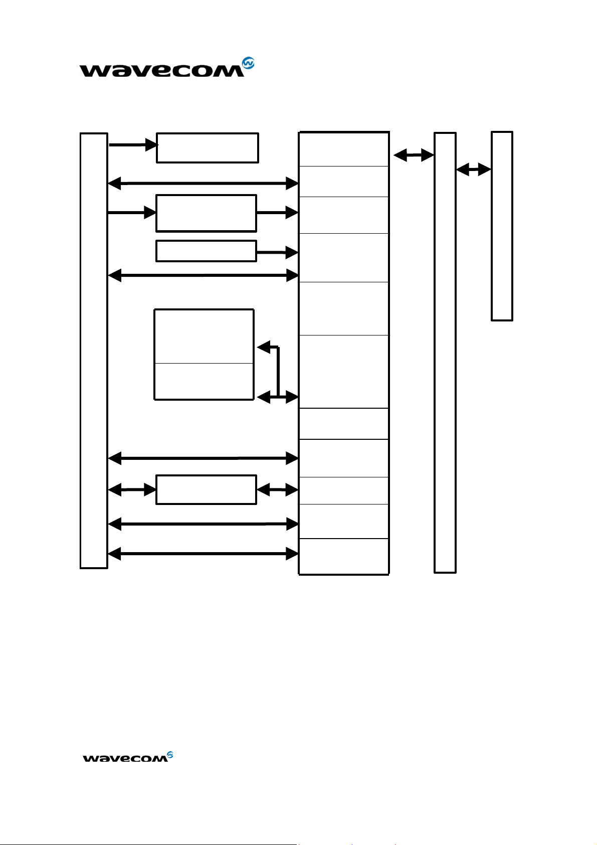
1.2 Functional description
WM_PRJ_Q2400_PTS_002 - 003
14th April 2003
G
E
N
E
R
A
L
P
U
R
P
O
S
E
C
O
N
N
E
C
T
O
R
Pow er Supply
Battery
M anagement
SIM Supply
FLA SH
SRAM
RF Interface
I/O Con t roller
A/D Converter
SIM Controller
CPU
Memory
M anagement
Unit
R.T.C
RF
F
U
N
C
T
I
O
N
S
RF
C
O
N
N
E
C
T
I
O
N
Audio Interface
Figure 1: Functional architecture
GPSI or SPI
Controller
Vocoder
Keyb oard
Controller
UART 1 & 2
confidential ©
This document is the sole and exclusive property of WAVECOM. Not to be distributed or divulged without prior written
agreement.
Ce document est la propriété exclusive de WAVECOM. Il ne peut être communiqué ou divulgué à des tiers sans son
autorisation préalable.
Page : 10 / 61
Page 11

WM_PRJ_Q2400_PTS_002 - 003
14th April 2003
1.2.1 RF functionalities
The Radio Frequency (RF) functionalities comply with the Phase II E-GSM 900/DCS 1800 and GSM
850/PCS 1900 recommendation.
The frequencies are:
Q2406
• Rx (E-GSM 900): 925 to 960 MHz.
• Rx (DCS 1800): 1805 to 1880 MHz.
• Tx (E-GSM 900): 880 to 915 MHz.
• Tx (DCS 1800): 1710 to 1785 MHz.
Q2426
• Rx (GSM 850): 869 to 894 MHz.
• Rx (PCS 1900): 1930 to 1990 MHz.
• Tx (GSM 850): 824 to 849 MHz.
• Tx (PCS 1900): 1850 to 1910 MHz.
The Radio Frequency (RF) part is based on a specific dual band chip including :
• Low-IF Receiver,
• Dual RF (Radio Frequency) synthesizer,
• Digital IF to Baseband Converter,
• Offset PLL (Phase Lock Loop) transmitter,
• 1 (logarithmic) Power Amplifier (PA) controller,
• Dual band Power Amplifier (PA) module.
1.2.2 Baseband functionalities
The digital part of the WISMO Quik Q24x6 sub-series is based on a PHILIPS-VLSI chip (ONE C
GSM/GPRS Kernel).
This chipset is using a 0.25 µm mixed technology CMOS, which allows massive integration as well
as low current consumption.
confidential ©
This document is the sole and exclusive property of WAVECOM. Not to be distributed or divulged without prior written
agreement.
Ce document est la propriété exclusive de WAVECOM. Il ne peut être communiqué ou divulgué à des tiers sans son
autorisation préalable.
Page : 11 / 61
Page 12

WM_PRJ_Q2400_PTS_002 - 003
14th April 2003
1.3 Firmware
WISMO Quik Q24x6 sub-series is designed to be integrated into various types of applications such
as handsets or vertical applications (telemetry, multimedia,…).
For vertical applications, the firmware offers a set of AT commands to control the module (for further
information, refer to document [3]).
Please be aware that some of these interfaces can not be handled when using the WISMO
Quik Q24x6 sub-series driven by AT commands: LCD interface, auxiliary serial link interface
and SPI bus.
AAA TTT
This symbol is used to indicate the interfaces not available with AT commands.
These functions have then to be managed externally i.e using the main processor of the
application.
confidential ©
This document is the sole and exclusive property of WAVECOM. Not to be distributed or divulged without prior written
agreement.
Ce document est la propriété exclusive de WAVECOM. Il ne peut être communiqué ou divulgué à des tiers sans son
autorisation préalable.
Page : 12 / 61
Page 13

WM_PRJ_Q2400_PTS_002 - 003
14th April 2003
2 Interfaces
Note:
Some of the WISMO interface signals are multiplexed in order to limit number of pins but this
architecture implies some limitation.
For example, in case of using SPI bus, 2-wire bus cannot be used.
Warning:
All external signals must be inactive when the WISMO module is OFF to avoid any damage
when starting and allow WISMO module to start correctly.
2.1 General Purpose Connector (GPC)
A 60-pin connector, with 0.5 mm pitch, is provided to interface the WISMO Quik Q24x6 sub-series
with a board containing either a LCD module, or a keyboard, or a SIM connector, or a battery
connection...
The interfaces available on the GPC are described in the next paragraphs.
The GPC is made by KYOCERA / AVX group with the following reference:
14 5087 060 930 861.
The matting connector has the following reference:
24 5087 060 X00 861.
For further details, refer to paragraph 4.4 General Purpose Connector data sheet.
confidential ©
This document is the sole and exclusive property of WAVECOM. Not to be distributed or divulged without prior written
agreement.
Ce document est la propriété exclusive de WAVECOM. Il ne peut être communiqué ou divulgué à des tiers sans son
autorisation préalable.
Page : 13 / 61
Page 14
WM_PRJ_Q2400_PTS_002 - 003
V
V
14th April 2003
2.2 Power supply
2.2.1 General description
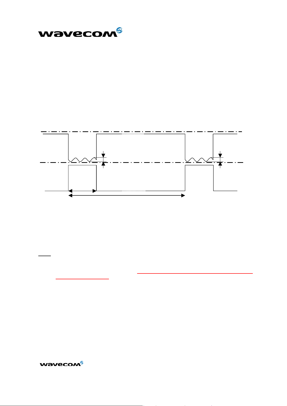
The power supply is one of the key issues in the design of a GSM terminal. Due to the bursted
emission in GSM / GPRS, the power supply must be able to deliver high current peaks in a short
time. During these peaks the ripple (U
in table “Power Supply Voltage” hereafter.
In communication mode, a GSM/GPRS class 2 terminal emits 577 µs radio bursts every 4.615 ms.
In communication mode, a GPRS class 10 terminal emits 1154 µs radio bursts every 4.615 ms.
) on the supply voltage must not exceed the limits specified
ripp
VBA TT
IBATT
(1)
or VDD if connected to VBATT
(1 )
Uripp
t = 577 µs
T = 4.615 ms
Figure 2: Typical power supply voltage in GSM mode
Two different inputs are provided for the power supply:
• the first one, VBATT is used to supply the RF part,
• the second one, VDD is used to supply the baseband part.
Notes
:
• It is possible to connect VBATT to VDD.
Uripp
max
min
• In case of separate power supplies, they have to be in the same state i.e both active or
inactive at the same time.
VBATT: supplies directly the RF components with 3.6 V. It is essential to keep a minimum voltage
ripple at this connection in order to avoid any phase error. The RF Power Amplifier current (2.0 A
peak in GSM /GPRS mode with a 50 Ohms RF output flows with a ratio of:
• 1/8 of the time (around 577 µs every 4.615 ms for GSM/GPRS class 2),
• 2/8 of the time (around 1154 µs every 4.615 ms for GSM/GPRS class 10).
The rising time is around 10 µs.
VDD: supplies the +2.8 V ballast regulators of the WISMO module. It is essential to keep the voltage
over 3.1 volts.
The WISMO module shielding case is the grounding. The ground has to be connected on the mother
board through a complete layer on the PCB.
confidential ©
This document is the sole and exclusive property of WAVECOM. Not to be distributed or divulged without prior written
agreement.
Ce document est la propriété exclusive de WAVECOM. Il ne peut être communiqué ou divulgué à des tiers sans son
autorisation préalable.
Page : 14 / 61
Page 15
WM_PRJ_Q2400_PTS_002 - 003
14th April 2003
Power Supply Voltage
V
VBATT
VDD
V
MIN
3.3 V (*) 3.6 V 4.5 V (**) 50 mVpp for freq<200 kHz
3.1 V 4.5 V 100 mVpp
V
NOM
MAX
Ripple max (U
500 µVpp for freq>200 kHz
ripp
)
(*): This value has to be guaranteed during the burst (with 2.0 A Peak in GSM or GPRS mode).
(**): max operating Voltage Stationary Wave Ratio (VSWR) 2:1.
When supplying the module with a battery, the total impedance (battery+contacts+protections+PCB)
should be < 150 mOhms to limit voltage drop-out within emission burst.
Refer to document [1] for further information about power supply design.
2.2.2 Power consumption
The following information is given assuming a 50 Ω RF output.
Power consumption in OFF mode
(module supplied, OFF state, no software running)
Conditions I
Overall consumption
Off 5 µA 10 µA
I
NOM
MAX
VBATT + VDD
confidential ©
This document is the sole and exclusive property of WAVECOM. Not to be distributed or divulged without prior written
agreement.
Ce document est la propriété exclusive de WAVECOM. Il ne peut être communiqué ou divulgué à des tiers sans son
autorisation préalable.
Page : 15 / 61
Page 16
WM_PRJ_Q2400_PTS_002 - 003
14th April 2003
Power consumption in E-GSM/GPRS 900 MHz and GSM/GPRS 850 MHz mode
class 10
Conditions I
VBATT+VDD
During TX bursts @Pcl5 1.60 A peak 1.8 A peak
During RX bursts
Average 1Rx/1Tx @Pcl5 250 mA 300 mA
Average 1Rx/1Tx @Pcl8 190 mA 200 mA
Average GPRS Cl 10 (3Rx/2Tx)
@Pcl5
Average GPRS Cl 10 (3Rx/2Tx)
@Pcl8
Average Idle mode 3 mA 7 mA
Power Control Level: Pcl5=2 W typ.; Pcl8=0.5 W typ.
Power consumption in GSM/GPRS 1800 MHz and
GSM/GPRS 1900 MHz mode class 10
Conditions I
VBATT+VDD
During TX bursts @Pcl0 1 A peak 1.5 A peak
During RX bursts
Average 1Rx/1Tx @Pcl0 190 mA 235 mA
Average 1Rx/1Tx @Pcl3 150 mA 180 mA
Average GPRS Cl 10 (3Rx/2Tx)
@Pcl0
Average GPRS Cl 10 (3Rx/2Tx)
@Pcl3
I
NOM
MAX
110 mA peak 115 mA peak
400 mA 510 mA
260 mA 300 mA
I
NOM
MAX
130 mA peak 140 mA peak
320 mA 410 mA
240 mA 270 mA
Average Idle mode 2 mA 6.5 mA
Power Control Level: Pcl0=1 W typ.; Pcl3=0.25 W typ.
Power Supply Pinout
Signal Pin number
+VBATT
VDD
GND
55, 57, 58, 59, 60
11
Shielding
The ground connection is done through the shielding the four legs have to be soldered to the
ground plane.
confidential ©
This document is the sole and exclusive property of WAVECOM. Not to be distributed or divulged without prior written
agreement.
Ce document est la propriété exclusive de WAVECOM. Il ne peut être communiqué ou divulgué à des tiers sans son
autorisation préalable.
Page : 16 / 61
Page 17
WM_PRJ_Q2400_PTS_002 - 003
2.3 Electrical information for digital I/O
All digital I/O comply with 3 Volts CMOS.
Operating conditions
Parameter I/O type Min Max Condition
14th April 2003
VIL
VIH
VOL
VOH
CMOS -0.5 V 0.8 V
CMOS 2.1 V 3.0 V
1X 0.2 V I
= -1 mA
OL
2X 0.2 V IOL = -2 mA
3X 0.2 V IOL = -3 mA
1X 2.6 V I
2X 2.6 V I
3X 2.6 V I
= 1 mA
OH
= 2 mA
OH
= 3 mA
OH
confidential ©
This document is the sole and exclusive property of WAVECOM. Not to be distributed or divulged without prior written
agreement.
Ce document est la propriété exclusive de WAVECOM. Il ne peut être communiqué ou divulgué à des tiers sans son
autorisation préalable.
Page : 17 / 61
Page 18
WM_PRJ_Q2400_PTS_002 - 003
A
14th April 2003
2.4 LCD interface
The WISMO Quik Q24x6 sub-series can be connected to a LCD module driver through either a SPI
bus or a two-wire interface.
2.4.1 SPI bus
The SPI bus includes a CLK signal (SPI_CLK), an I/O signal (SPI_IO) and an EN signal (SPI_EN)
complying with SPI bus standard.
Pin description
Signal Pin number I/O I/O type Description
SPI_CLK 10 O 1X SPI Serial Clock
SPI_IO 8 I/O CMOS / 1X SPI Data
SPI_EN * 28 O 1X SPI Enable
* Multiplexed with GPO3.
2.4.2 Two-wire interface
T
T
T
The two-wire interface includes a CLK signal (SCL) and a DATA signal (SDA) complying with a
standard 96 kHz interface. The maximum speed transfer is 400 kbits/s.
Pin description
Signal Pin number I/O I/O type Description
SCL 10 O 1X Serial Clock
SDA 8 I/O CMOS / 1X Serial Data
2.5 SPI Auxiliary bus
A second SPI Chip Enable (called SPI_AUX) has to be used to add a SPI peripheral to the WISMO
Quik Q24x6 sub-series.
Pin description
Signal Pin number I/O I/O type Description
SPI_CLK 10 O 1X SPI Serial Clock
SPI_IO 8 I/O CMOS / 1X SPI Data
SPI_AUX * 26 O 1X SPI Aux. Enable
* Multiplexed with GPO0.
confidential ©
This document is the sole and exclusive property of WAVECOM. Not to be distributed or divulged without prior written
agreement.
Ce document est la propriété exclusive de WAVECOM. Il ne peut être communiqué ou divulgué à des tiers sans son
autorisation préalable.
Page : 18 / 61
Page 19
WM_PRJ_Q2400_PTS_002 - 003
14th April 2003
2.6 Keyboard interface
Warning:
This interface is not FULLY available with AT commands:
An AT command allows to get the input key code (see AT+CMER command description). This
code has then to be processed by the application.
This interface provides 10 connections:
• 5 rows (ROW0 to ROW4),
• 5 columns (COL0 to COL4).
The scanning is a digital one, and the debouncing is done in the WISMO module. No discrete
components like R, C (Resistor, Capacitor) are needed.
Pin description
Signal Pin number I/O I/O type Description
ROW0 13 I/O CMOS / 1X Row scan
ROW1 15 I/O CMOS / 1X Row scan
ROW2 17 I/O CMOS / 1X Row scan
ROW3 19 I/O CMOS / 1X Row scan
ROW4 21 I/O CMOS / 1X Row scan
COL0 23 I/O CMOS / 1X Column scan
COL1 25 I/O CMOS / 1X Column scan
COL2 27 I/O CMOS / 1X Column scan
COL3 29 I/O CMOS / 1X Column scan
COL4 31 I/O CMOS / 1X Column scan
confidential ©
This document is the sole and exclusive property of WAVECOM. Not to be distributed or divulged without prior written
agreement.
Ce document est la propriété exclusive de WAVECOM. Il ne peut être communiqué ou divulgué à des tiers sans son
autorisation préalable.
Page : 19 / 61
Page 20

WM_PRJ_Q2400_PTS_002 - 003
14th April 2003
2.7 Main serial link (UART1)
A flexible 6-wire serial interface is available complying with V24 protocol signaling but not with V28
(electrical interface) due to a 2.8 Volts interface.
The signals are:
• TX data (CT103/TX),
• RX data (CT104/RX),
• Request To Send (CT105/RTS),
• Clear To Send (CT106/CTS),
• Data Terminal Ready (CT108-2/DTR),
• Data Set Ready (CT107/DSR).
The set of serial link signals can be required for GSM DATA services application and is generated
by the general purpose I/O provided by the WISMO module.
The 2 additional signals are Data Carrier Detect (CT109/DCD) and Ring Indicator (CT125/RI).
Pin description
Signal Pin number I/O I/O type Description
CT103/TXD1 39 I CMOS Transmit serial data
CT104/RXD1 32 O 1X Receive serial data
CT105/RTS1 30 I CMOS Request To Send
CT106/CTS1 37 O 1X Clear To Send
CT107/DSR1 36 O 1X Data Set Ready
CT108-2/DTR1 34 I CMOS Data Terminal Ready
CT109/DCD1 * 51 O CMOS / 2X Data Carrier Detect
CT125/RI1 ** 54 O CMOS / 2X Ring Indicator
CT102/GND Shielding legs Ground
* Multiplexed with GPIO3
** Multiplexed with GPIO2.
The rising time and falling time of the reception signals (mainly CT103) have to be less than 200 ns.
The WISMO Quik Q24x6 sub-series has been designed to be operated using all the serial interface
signals. In particular, it is necessary to use RTS and CTS signals for hardware flow control in order
to avoid data corruption during transmission.
2.8 Auxiliary serial link (UART2)
For future applications (e.g. Bluetooth connectivity) an auxiliary serial interface (UART2) will be
available on Q24x6A and Q24x6B products.
confidential ©
This document is the sole and exclusive property of WAVECOM. Not to be distributed or divulged without prior written
agreement.
Ce document est la propriété exclusive de WAVECOM. Il ne peut être communiqué ou divulgué à des tiers sans son
autorisation préalable.
Page : 20 / 61
Page 21

WM_PRJ_Q2400_PTS_002 - 003
14th April 2003
Warning:
The auxiliary serial link (UART2) is not available on Q24x6D and Q24x6E products (version
with 64 Mbits of Flash memory).
Pin description
Signal Pin
number
I/O I/O type Description Multiplexed
with
CT103 / TXD2 18 I 3X Receive serial data GPI
CT104 / RXD2 20 O CMOS Transmit serial data GPO2
CT106 / CTS2 24 I CMOS Clear To Send GPIO0
CT105 / RTS2 35 O 2X Request To Send GPIO5
2.9 SIM interface
2.9.1 General Description
5 signals are available:
• SIM_VCC: SIM power supply.
• SIM_RST: reset.
• SIM_CLK: clock.
• SIM_DATA: I/O port.
• SIM_PRES: SIM card detect.
The SIM interface controls a 3 V SIM card (and a 5 V SIM card through an external SIM driver, refer
to document [1] for more details).
This interface is fully compliant with GSM 11.11 recommendations concerning SIM functions.
Pin description
Signal Pin number I/O I/O type Description
SIM_CLK 3 O 2X SIM Clock
SIM_RST 5 O 2X SIM Reset
SIM_DATA 7 I/O CMOS / 3X SIM Data
SIM_VCC 9 O SIM Power Supply
SIM_PRES 50 I CMOS SIM Card Detect
confidential ©
This document is the sole and exclusive property of WAVECOM. Not to be distributed or divulged without prior written
agreement.
Ce document est la propriété exclusive de WAVECOM. Il ne peut être communiqué ou divulgué à des tiers sans son
autorisation préalable.
Page : 21 / 61
Page 22

WM_PRJ_Q2400_PTS_002 - 003
14th April 2003
Electrical Characteristics
Parameter Conditions Min Typ Max Unit
IIH = ± 20 µA
IIL = 1 mA
Source current =
20 µA
Sink current =
-200 µA
I
<= 6 mA
SIMVCC
0.7xSIM_VCC V
0.3xSIM_VCC V
SIM_VCC – 0.1V V
0.1 V
2.70 2.80 2.85 V
SIM_DATA VIH
SIM_DATA VIL
SIM_RST,
SIM_DATA
SIM_CLK V
OH
SIM_RST,
SIM_DATA
SIM_CLK V
OL
SIM_VCC* Output
Voltage
SIM_CLK
Loaded with 30 pF
50 ns
Rise/Fall Time
SIM_RST,
Loaded with 30 pF
1 µs
SIM_DATA
Rise/Fall Time
SIM_CLK
Loaded with 30 pF
3.25 MHz
Frequency
(*): given for a 3 V interface. An external SIM driver is needed to handle 5 V SIMs.
Note for SIM_PRES connection
:
• When not used SIM_PRES has to be tied to VCC.
• When used, a low to high transition means that the SIM card is inserted and a high to low
transition means that the SIM card is removed.
2.9.2 SIM 3/5V management
1
The WISMO Quik Q24x6 sub-series module is designed to interface with 3 V SIMs only
.
Nevertheless, it is possible to manage 3 V and 5 V SIM cards using an external level shifter (refer to
customer design guidelines [1]). In this case, depending on the type of SIM detected, the module
firmware triggers the GPO0 output signal (pin #26) in order to properly set the external SIM driver
level (3V or 5V).
1
Most of the GSM operators have been providing 3 V SIMs since 1998.
confidential ©
This document is the sole and exclusive property of WAVECOM. Not to be distributed or divulged without prior written
agreement.
Ce document est la propriété exclusive de WAVECOM. Il ne peut être communiqué ou divulgué à des tiers sans son
autorisation préalable.
Page : 22 / 61
Page 23

WM_PRJ_Q2400_PTS_002 - 003
A
2.10 General Purpose Input/Output
The WISMO Quik Q24x6 sub-series provides:
• 6 General Purpose I/O,
• 4 General Purpose Outputs,
• 1 General Purpose Input.
They are used to control any external device such as a LCD or a Keyboard backlight.
Pin description
14th April 2003
Signal Pin
number
GPIO0 24 I/O CMOS / 2X General Purpose I/O CT106/CTS2
GPIO4 53 I/O CMOS / 2X General Purpose I/O
GPIO5 35 I/O CMOS / 2X General Purpose I/O CT105/RTS2
GPO0 26 O 3X General Purpose O SPI_AUX
GPO1 22 O 3X General Purpose O
GPO2 20 O 1X General Purpose O CT104/RXD2
GPI 18 I CMOS General Purpose I CT103/TXD2
GPO3 28 O CMOS General Purpose O SPI_EN
T
T
T
The following GPIOs are not available (reserved) in case of module running with the AT commands
firmware:
Signal Pin
number
GPIO1 52 I/O CMOS / 2X General Purpose I/O FLASH LED(*)
GPIO2 54 I/O CMOS / 2X General Purpose I/O CT125/RI1
I/O I/O type Description Multiplexed with
I/O I/O type Description Multiplexed with
GPIO3 51 I/O CMOS / 2X General Purpose I/O CT109/DCD1
(*) The FLASH LED signal can be used to drive a LED through an open-collector transistor
according to the module activity status.
2.11 Activity status indication
The activity status indication signal can be used to drive a LED through an open-collector transistor
according to the module activity status.
confidential ©
This document is the sole and exclusive property of WAVECOM. Not to be distributed or divulged without prior written
agreement.
Ce document est la propriété exclusive de WAVECOM. Il ne peut être communiqué ou divulgué à des tiers sans son
autorisation préalable.
Page : 23 / 61
Page 24

WM_PRJ_Q2400_PTS_002 - 003
LED status WISMO Quik Q24x6 sub-series status
OFF Module in download mode or module OFF
14th April 2003
ON
Permanent Module switched ON, not registered on the network
Slow flash
Module switched ON, registered on the network
LED ON for 200 ms, OFF
for 2 s
Quick flash
LED ON for 200 ms, OFF
Module switched ON, registered on the network,
communication in progress
for 600 ms
Signal Pin number I/O I/O type Description
FLASH LED 52 I/O CMOS / 2X General Purpose I/O
2.12 Analog to Digital Converter (ADC)
An Analog to Digital Converter is provided by the WISMO module. This converter is a 10-bit
resolution, ranging from 0 to 2.8 V.
Pin description
Signal Pin number I/O I/O type Description
AUXV0 33 I Analog A/D converter
Electrical Characteristics
Parameter Min Max Unit
Resolution 10 bits
Sampling rate 90.3 Ksps/s
Input signal range 0 2.8V V
ADC Reference Accuracy 0.75 2 %
Integral Accuracy +/- 1 LSB
Differential Accuracy +/- 1 LSB
Input Impedance ( R ) 10
MΩ
Input Impedance ( C ) 100 nF
confidential ©
This document is the sole and exclusive property of WAVECOM. Not to be distributed or divulged without prior written
agreement.
Ce document est la propriété exclusive de WAVECOM. Il ne peut être communiqué ou divulgué à des tiers sans son
autorisation préalable.
Page : 24 / 61
Page 25

WM_PRJ_Q2400_PTS_002 - 003
14th April 2003
2.13 Audio interface
Two different microphone inputs and two different speaker outputs are supported.
The WISMO Quik Q24x6 sub-series also includes an echo cancellation feature which allows handsfree function.
In some case, ESD protection must be added on the audio interface lines.
2.13.1 Microphone inputs
The MIC2 inputs already include the biasing for an electret microphone allowing an easy connection
to a handset.
The MIC1 inputs do not include an internal bias. MIC1/SPK1 is then appropriate for a hands-free
system or a handset with biasing external to the module.
2.13.1.1 Common microphone inputs characteristics
The connection can be either differential or single-ended but using a differential connection in order
to reject common mode noise and TDMA noise is strongly recommended. When using a single-
ended connection, be sure to have a very good ground plane, a very good filtering as well as
shielding in order to avoid any disturbance on the audio path.
Internal audio filter characteristics
Frequency Gain
0-150 Hz < -22 dB
150-180 Hz < -11 dB
180-200 Hz < -3 dB
200-3700 Hz 0 dB
>4000 Hz < -60 dB
The gain of MIC inputs is internally adjusted and can be tuned from 30 dB to 51 dB using an AT
command (refer to AT commands documentation [3]).
confidential ©
This document is the sole and exclusive property of WAVECOM. Not to be distributed or divulged without prior written
agreement.
Ce document est la propriété exclusive de WAVECOM. Il ne peut être communiqué ou divulgué à des tiers sans son
autorisation préalable.
Page : 25 / 61
Page 26

WM_PRJ_Q2400_PTS_002 - 003
Microphone gain vs Max input voltage (using controller 1*)
Transmit Gain (dB) Max Vin (mVrms)
+30 43.80
+33 31.01
+36 21.95
+39 15.54
+42 11
+45 7.79
+48 5.51
+51 3.9
(*) for more details, refer to AT commands documentation [3]
Microphone gain vs Max input voltage (using controller 2*)
Transmit Gain (dB) Max Vin (mVrms)
- 6.5 3031
-6.0 2861
14th April 2003
… …
0.0 1434
… …
+9.5 480
+10.0 454
+ 30.3 43.80
+ 30.8 41.36
… …
+ 50.8 4.14
+ 51.3 3.90
(*) for more details, refer to AT commands documentation [3]
confidential ©
This document is the sole and exclusive property of WAVECOM. Not to be distributed or divulged without prior written
agreement.
Ce document est la propriété exclusive de WAVECOM. Il ne peut être communiqué ou divulgué à des tiers sans son
autorisation préalable.
Page : 26 / 61
Page 27

WM_PRJ_Q2400_PTS_002 - 003
14th April 2003
2.13.1.2 Main Microphone Inputs (MIC2)
The MIC2 inputs are differential ones. They already include the convenient biasing for an electret
microphone (0.5 mA and 2 Volts). This electret microphone can be directly connected on these
inputs.
The impedance of the microphone 2 has to be around 2 kΩ. These inputs are the standard ones for
an handset design while MIC1 inputs can be connected to an external headset or a hands-free kit.
AC coupling is already embedded in the module.
Pin description
Signal Pin # I/O I/O type Description
MIC2P 46 I Analog Microphone 2 positive input
MIC2N 48 I Analog Microphone 2 negative input
2.13.1.3 Auxiliary Microphone Inputs (MIC1)
The MIC1 inputs are differential and do not include internal bias. To use these inputs with an electret
microphone, bias has to be generated outside the WISMO Quik Q24x6 sub-series module according
to the characteristic of this electret microphone. These inputs are the standard ones used for an
external headset or a hands-free kit.
The impedance of the microphone 1 has to be around 2 kΩ. These inputs are provided for an
external headset or a hands-free kit.
AC coupling is already embedded in the module.
Pin description
Signal Pin # I/O I/O type Description
MIC1P 42 I Analog Microphone 1 positive input
MIC1N 44 I Analog Microphone 1 negative input
confidential ©
This document is the sole and exclusive property of WAVECOM. Not to be distributed or divulged without prior written
agreement.
Ce document est la propriété exclusive de WAVECOM. Il ne peut être communiqué ou divulgué à des tiers sans son
autorisation préalable.
Page : 27 / 61
Page 28

WM_PRJ_Q2400_PTS_002 - 003
14th April 2003
2.13.2 Speaker outputs
2.13.2.1 Common speaker outputs characteristics
The connection can be differential or single-ended but using a differential connection to reject
common mode noise and TDMA noise is strongly recommended. Morover in single-ended mode, ½
of the power is lost. When using a single-ended connection, be sure to have a very good ground
plane, a very good filtering as well as shielding in order to avoid any disturbance on the audio path.
Speaker outputs SPK1 and SPK2 are push-pull amplifiers and can be loaded down to 150 Ohms
and up to 1 nF (see details in table Speaker gain vs Max output voltage).
Impedance of the speaker amplifier output in differential mode is :
R ≤ 1Ω +/-10 %.
These outputs are differential and the output power can be adjusted by step of 2 dB. The output can
be directly connected to a speaker.
Using a single-ended connection also includes losing half of the output power compared to a
differential connection.
The gain of the speaker outputs is internally adjusted and can be tuned using an AT command.
Speaker gain vs Max output voltage
Receive Gain (dB) (*) Max output level (Vrms)
+2 1.74 150
0 1.38 50
-2 1.099 32
-4 0.873 32
-6 0.693 32
-8 0.551 32
-10 0.437 32
-12 0.347 32
-14 0.276 32
-16 0.219 32
-18 0.174 32
-20 0.138 32
-22 0.110 32
-24 0.087 32
-26 0.069 32
(*) analog gain: might not be significant
Max.speaker load (Ω)
confidential ©
This document is the sole and exclusive property of WAVECOM. Not to be distributed or divulged without prior written
agreement.
Ce document est la propriété exclusive de WAVECOM. Il ne peut être communiqué ou divulgué à des tiers sans son
autorisation préalable.
Page : 28 / 61
Page 29

2.13.2.2 Speaker 2 Outputs
Signal Pin # I/O I/O type Description
SPK2P 45 O Analog Speaker 2 positive output
SPK2N 47 O Analog Speaker 2 negative output
2.13.2.3 Speaker 1 Outputs
Signal Pin # I/O I/O type Description
SPK1P 41 O Analog Speaker 1 positive output
SPK1N 43 O Analog Speaker 1 negative output
2.13.3 Buzzer Output
WM_PRJ_Q2400_PTS_002 - 003
14th April 2003
Pin description
Pin description
The buzzer output (BUZ) is a digital one. A buzzer can be directly connected between this output
and VBATT. The maximum current is 80 mA (PEAK).
Pin description
Signal Pin # I/O I/O type Description
BUZ 49 O Analog
(open collector)
Buzzer output
Operating conditions
Parameter Condition Min Max Unit
VOL I
I
VBATT = VBATTmax 80
PEAK
I
AVERAGE
VBATT = VBATTmax 40
AVERAGE
= 40 mA 0.6
V
mA
mA
confidential ©
This document is the sole and exclusive property of WAVECOM. Not to be distributed or divulged without prior written
agreement.
Ce document est la propriété exclusive de WAVECOM. Il ne peut être communiqué ou divulgué à des tiers sans son
autorisation préalable.
Page : 29 / 61
Page 30

WM_PRJ_Q2400_PTS_002 - 003
14th April 2003
2.14 Battery charging interface
2.14.1 Hardware description
The WISMO module supports one battery charging circuit for Li-Ion batteries.
This circuit uses an interface which consists of a current source inputs (CHG_IN) where the constant
current has to flow in order to charge the battery.
This current value depends on the battery capacity. It is recommended to provide a current equal to
the value of the capacity plus 50 mA. For a 550 mA battery the current will be 600 mA. The
maximum current is 800 mA.
A specific AT command (AT+WBCM), available from 4.3 level, allows to manage the battery charge
(start and stop the charge, enable or disable unsolicited Battery Charge Indications and set the
battery charge parameters).
The WISMO module monitors the battery voltage to detect the end of the charge.
The WISMO module also monitors the temperature of the battery through the BAT_TEMP pin which
has to be connected to a temperature sensor inside the battery (a NTC resistor for instance).
Pin description
Signal Pin number I/O I/O type Description
CHG_IN 1, 2, 4 I Supply Current source input
BAT_TEMP 38 I Analog A/D converter
confidential ©
This document is the sole and exclusive property of WAVECOM. Not to be distributed or divulged without prior written
agreement.
Ce document est la propriété exclusive de WAVECOM. Il ne peut être communiqué ou divulgué à des tiers sans son
autorisation préalable.
Page : 30 / 61
Page 31

WM_PRJ_Q2400_PTS_002 - 003
14th April 2003
Electrical Characteristics
Parameter Min Max Typ Unit
BAT_TEMP resolution 10 bits
BAT_TEMP sampling rate 90.3 Ksps/s
BAT_TEMP Input Impedance ( R ) 4.7
kΩ
BAT_TEMP Input Impedance ( C ) 100 nF
CHG_IN Voltage (for I=Imax) 5.1* 5.5 V
CHG_IN Current 800 mA
BAT_TEMP Input signal range 2.8 Vpp
* To be parametrized as per battery manufacturer
2.14.2 Li-ion charging procedure
A constant current source has to be provided through CHG_IN inputs in order to charge the Li-ion
battery, and BAT_TEMP input has to be connected to a battery temperature sensor. During this
procedure the voltage of the battery is accurately monitored.
The Li-ion charging involves two phases:
• During the first phase, the battery is charged with a constant current until its voltage reaches
4.1 V*,
• During the second phase, the constant current is pulsed by the module. The width and the
frequency of the pulse change during this phase in order to ensure a safety charge.
The battery is considered as fully charged when, after a pulse, the voltage remains at a 4.1 V*
during more than 10 s.
The Li-ion battery must have an included safety circuit to avoid any discharge or overcharge. This
circuit is delivered by the manufacturer inside the battery pack. The impedance of this safety circuit
has to be the lowest possible in order to reduce the drop-out of the voltage. This drop-out is due to
the RF Power Amplifier current (up to 2.0 A). A maximum of 150 mΩ is required.
(*): To be parametrized as per battery manufacturer
confidential ©
This document is the sole and exclusive property of WAVECOM. Not to be distributed or divulged without prior written
agreement.
Ce document est la propriété exclusive de WAVECOM. Il ne peut être communiqué ou divulgué à des tiers sans son
autorisation préalable.
Page : 31 / 61
Page 32

WM_PRJ_Q2400_PTS_002 - 003
14th April 2003
2.15 ON / ~OFF
2.15.1 General description
This input is used to switch ON or OFF the WISMO module.
A high level signal has to be provided on the pin ON/~OFF to switch ON the module.
The level of the voltage of this signal has to be maintained between 2.4 V and VDD during a
minimum of 1 s.
This signal can be left at high level until switch OFF.
To be able to switch OFF the module, the pin ON/~OFF has to be released. Through the firmware,
the module can be switched OFF (using the AT+CPOF command).
Pin description
Signal Pin number I/O I/O type Description
ON/∼OFF
Input Impedance ( R ) 10
Input Impedance ( C ) 50 pF
6 I CMOS Module Power ON/OFF
Electrical Characteristics
Parameter Min Max Unit
kΩ
Operating conditions
Parameter I/O type Min Max Unit
VIL 0 V 0.6 V V
VIH 2.4 V VDD+0.5 V V
confidential ©
This document is the sole and exclusive property of WAVECOM. Not to be distributed or divulged without prior written
agreement.
Ce document est la propriété exclusive de WAVECOM. Il ne peut être communiqué ou divulgué à des tiers sans son
autorisation préalable.
Page : 32 / 61
Page 33

WM_PRJ_Q2400_PTS_002 - 003
A
14th April 2003
2.15.2 Operating sequences
2.15.2.1 Power ON
Once the module is supplied by the power source, the application must set the ON/~OFF signal to
high to start the module power ON sequence.
The ON/~OFF signal must be held for 1 s minimum. After this time, an internal mechanism keeps it
on hold. During the power ON sequence, an internal reset is automatically performed by the module
for 240 ms (typical). During this phase, any external reset should be avoided.
Once the initialisation is complete (timing is SIM and network dependent) the AT interface answers
« OK » to the application
2
. For further details, please refer to the AT commands documentation
(AT+WIND, AT+WAIP)
POW ER SUPPLY
ON/~OFF
INTERN A L RST
Module OFF
I
ST A TE O F T H E M OD ULE
I
= overall current consumption (Base Band + RF part)
BB+RF
BB+RF
< 10 µA
T
on/off-hold
(1 s m in)
T
rst
(240 ms typ)
RESET m od e
I
=20 to 40 mA
BB+RF
SIM and Network dependent
M odule ON
I
<120 mA
BB+RF
(no loc. update)
T answ ers « OK »
Module READY
Figure 3: Power-ON sequence diagram (no PIN code activated)
2
For this, the application has to send AT↵. If the application manages hardware flow control, the AT command can be sent
during the initialisation phase. Another solution is to use the AT+WIND command to get an unsolicited status from the
module.
confidential ©
This document is the sole and exclusive property of WAVECOM. Not to be distributed or divulged without prior written
agreement.
Ce document est la propriété exclusive de WAVECOM. Il ne peut être communiqué ou divulgué à des tiers sans son
autorisation préalable.
Page : 33 / 61
Page 34

WM_PRJ_Q2400_PTS_002 - 003
A
14th April 2003
2.15.2.2 Power OFF
To properly power OFF the module, the application must set the ON/~OFF signal to low and then
send the AT+CPOF command to de-register from the network and switch off the module. Once the
« OK » response is issued by the module, the power supply can be switched off.
POW ER SUPPLY
ON/
OFF
~
AT COM M AND
ST A TE OF T H E M OD U LE
I
= overall current consumption (Base Band + RF part)
BB+RF
Module
READ Y
T+CPOF
Netw ork dependent
OK response
Module OFF
I
<100 µA
BB+RF
Figure 4: Power-OFF sequence diagram
2.16 BOOT (optional)
This input can be used to download a software in the Flash memory of the WISMO module.
For the applications based on AT commands, this is a backup download procedure only (refer to
document [1] Customer Design Guidelines).
The internal boot procedure is started when this pin is low during the reset of the module.
In normal mode this pin has to be left open. In Internal boot mode, low level has to be set through a
1KΩ resistor. If used, this input has to be driven by an open collector or an open drain output:
• BOOT pin 12 = 0, for download mode,
• BOOT pin 12 = 1, for normal mode.
Pin description
Signal Pin number I/O I/O type Description
BOOT 12 I CMOS Flash Downloading
Note : The nominal firmware download procedure is using the X-modem
confidential ©
This document is the sole and exclusive property of WAVECOM. Not to be distributed or divulged without prior written
agreement.
Ce document est la propriété exclusive de WAVECOM. Il ne peut être communiqué ou divulgué à des tiers sans son
autorisation préalable.
Page : 34 / 61
Page 35

WM_PRJ_Q2400_PTS_002 - 003
14th April 2003
2.17 Reset signal (~RST)
2.17.1 General description
This signal is used to force a reset procedure by providing low level during at least 500 µs.
This signal has to be considered as an emergency reset only. A reset procedure is automatically
driven by an internal hardware during the power-up sequence.
This signal can also be used to provide a reset to an external device. It then behaves as an output. If
no external reset is necessary this input can be left open. If used (emergency reset), it has to be
driven by an open collector or an open drain output:
• ∼RST pin 14 = 0, for Module Reset,
• ∼RST pin 14 = 1, for normal mode.
Pin description
Signal Pin number I/O I/O type Description
∼RST
14 I/O SCHMITT Module Reset
Electrical Characteristics
Parameter Min Max Unit
Input Impedance ( R ) 4.7
Input Impedance ( C ) 10 nF
Operating conditions
Parameter Min Max Condition
*VT- 1.1 V 1.2 V
*VT+ 1.7 V 1.9 V
VOL 0.4 V IOL = -50 µA
VOH 2.0 V IOH = 50 µA
* V
Additional comments on RESET:
The RESET process is activated either
Hysteresis thresholds
T-, VT+ :
by the external ~RST signal or by an internal signal (coming
from a RESET generator). This automatic reset is activated at Power-up.
kΩ
The module remains in RESET mode as long as the ~RST signal is held low.
This signal should be used only for “emergency” resets
.
A software reset is always preferred to a hardware reset.
confidential ©
This document is the sole and exclusive property of WAVECOM. Not to be distributed or divulged without prior written
agreement.
Ce document est la propriété exclusive de WAVECOM. Il ne peut être communiqué ou divulgué à des tiers sans son
autorisation préalable.
Page : 35 / 61
Page 36

WM_PRJ_Q2400_PTS_002 - 003
µ
A
14th April 2003
2.17.2 Reset sequence
To activate the « emergency » reset sequence, the ~RST signal has to be set to low for 500 µs
minimum.
As soon as the reset is complete, the AT interface answers « OK » to the application. For this, the
application has to send AT↵. If the application manages hardware flow control, the AT command
can be sent during the initialisation phase. Another solution is to use the AT+WIND command to get
an unsollicited status from the module.
For further details, refer to AT commands documentation [3].
EXTERN A L RST
Module READY
ST A TE OF T H E M OD U LE
M in:500
Typ:2 m s
RESET m od e
I
BB+RF
to 40 mA
SIM and netw ork dependent
s
=20
Module ON
I
<120 m A
BB+RF
w ithout loc update
T answ ers “ OK”
Module READY
Figure 5: Reset sequence diagram
2.18 External Interrupt (~INTR)
The WISMO module provides an external interrupt input ~INTR. This input is very sensitive and an
interrupt is activated on high to low edge. If this signal is not used it can be left open. If used this
input has to be driven by an open collector or an open drain output.
This input is used for instance to power OFF automatically the module.
Pin description
Signal Pin number I/O I/O type Description
~INTR
16 I CMOS External Interrupt
Electrical characteristics
Parameter Min Max Unit
VIL -0.5 0.7 Volt
VIH 2.2 3.0 Volt
confidential ©
This document is the sole and exclusive property of WAVECOM. Not to be distributed or divulged without prior written
agreement.
Ce document est la propriété exclusive de WAVECOM. Il ne peut être communiqué ou divulgué à des tiers sans son
autorisation préalable.
Page : 36 / 61
Page 37

WM_PRJ_Q2400_PTS_002 - 003
14th April 2003
2.19 VCC output
This output can be used to power some external functions. VCC has to be used as a digital power
supply. This power supply is available when the module is ON.
Pin description
Signal Pin number I/O I/O type Description
VCC 40 O Supply Digital supply
Operating conditions
Parameter Condition Min Max Unit
Output voltage
Output Current
I = 10 mA 2.74 2.86 V
10 mA
2.20 Real Time Clock Supply (VCC_RTC)
VCC_RTC input is used to provide a back-up power supply for the internal Real Time Clock. The
RTC is supported by the module when powered on but a back-up power supply is needed to save
date and time information when the module is switched off.
If the RTC is not used this pin can be left open.
Pin description
Signal Pin number I/O I/O type Description
VCC_RTC 56 I/O Supply RTC Back-up supply
Operating conditions
Parameter Condition Min Max Unit
Input voltage 2 2.75 V
Input Current VCC=0 V; t° = +25 °C
3 µA
VCC_RTC=2.5 V
Input Current VCC=0 V; t°:-20 °C / +55 °C
10 µA
VCC_RTC=2.5 V
Output voltage 2.4 2.75 V
Output current 2 mA
2.21 RF interface
The impedance is 50 Ohms nominal and the DC impedance is 0 Ohm.
confidential ©
This document is the sole and exclusive property of WAVECOM. Not to be distributed or divulged without prior written
agreement.
Ce document est la propriété exclusive de WAVECOM. Il ne peut être communiqué ou divulgué à des tiers sans son
autorisation préalable.
Page : 37 / 61
Page 38

WM_PRJ_Q2400_PTS_002 - 003
14th April 2003
2.21.1 RF connections
2.21.1.1 General
There are two possible ways to connect an antenna to the module:
• The antenna can be directly connected to the module on the "Antenna pad" by using a spring
contact.
• The antenna can be connected to the module through a coaxial cable. The coaxial cable is
connected to both the "Round pad" and the "Ground pad".
Spring contact
Two land patterns set on the PCB support the RF connection which can be used by the
application through spring contacts or a soldered RF cable.
Since no standard spring contact is available for WISMO Quik Q24x6 sub-series, this solution
requires a specific part to be developed.
Soldered solution
The soldered solution will preferably be based on a RG178 coaxial cable.
Ground
pad
Antenna
pad
Antenna pad
Antenna connection by spring contact. Antenna connection by coaxial cable.
Figure 6: Antenna connection
Note:
• The WISMO Quik Q24x6 sub-series does not include any antenna switch for a car kit but
this function can be implemented externally and it can be driven using a GPIO.
• The antenna cable and connector should be chosen in order to minimise losses in the
frequency bands used for GSM 850/E-GSM 900MHz and DCS 1800/PCS 1900MHz.
• 0.5 dB can be considered as a maximum value for loss between the module and an external
connector.
2.21.1.2 Antenna directly connected to the module: matching circuit
The goal of the matching circuit is to link the antenna (impedance ZA) to the receiver and transmitter
access of the module (impedance ZL = 50 Ohm real).
confidential ©
This document is the sole and exclusive property of WAVECOM. Not to be distributed or divulged without prior written
agreement.
Ce document est la propriété exclusive de WAVECOM. Il ne peut être communiqué ou divulgué à des tiers sans son
autorisation préalable.
Page : 38 / 61
Page 39

WM_PRJ_Q2400_PTS_002 - 003
14th April 2003
Z
A
M atching
circuit
ZL= 50 Ohm
Receiv er +
WISMO module
Figure 7: Matching circuit
The matching circuit is composed by four elements implemented (see figure above) on the module
connecting the "Antenna pad" to the "Round pad" (access to the receiver and the transmitter).
The four elements of the matching circuit are not yet defined, and depend on each antenna and
mechanical integration.
The matching circuit must be verified for each frequency bandwidth:
:
Q2406
900 MHz (880 to 960 MHz),
1800 MHz (1710 to 1880 MHz).
Q2426
:
850 MHz (824 to 894 MHz),
1900 MHz (1850 to 1990 MHz).
CM2
CM4
CM3
CM1
Figure 8: WISMO Q24x6 sub-series antenna matching circuit (bottom view)
confidential ©
This document is the sole and exclusive property of WAVECOM. Not to be distributed or divulged without prior written
agreement.
Ce document est la propriété exclusive de WAVECOM. Il ne peut être communiqué ou divulgué à des tiers sans son
autorisation préalable.
Page : 39 / 61
Page 40

WM_PRJ_Q2400_PTS_002 - 003
A
14th April 2003
ntenna pad
Round pad
GND
= 50Ω
Z
CM 1 CM 3
L
GND GND
CM 2
CM 4
Figure 9: Electrical diagram for the WISMO Quik Q24x6 sub-series
2.21.2 RF performances
RF performances are compliant with the ETSI recommendation GSM 05.05.
The main parameters for Receiver are:
• GSM850 Reference Sensitivity (Q2426) = -104 dBm Static & TUHigh
• E-GSM900 Reference Sensitivity (Q2406)= -104 dBm Static & TUHigh
• DCS1800 Reference Sensitivity (Q2406)= -102 dBm Static & TUHigh
• PCS1900 Reference Sensitivity (Q2426)= -102 dBm Static & TUHigh
• Selectivity @ 200 kHz: > +9 dBc
• Selectivity @ 400 kHz: > +41 dBc
• Linear dynamic range: 63 dB
• Co-channel rejection: >= 9 dBc
And for Transmitter:
• Maximum output power (E-GSM 900 & GSM850): 33 dBm +/- 2 dB at ambient temperature,
• Maximum output power (DCS1800 & PCS1900): 30 dBm +/- 2 dB at ambient temperature,
• Minimum output power (E-GSM 900 & GSM850): 5 dBm +/- 5 dB at ambient temperature,
• Minimum output power (DCS1800 & PCS1900): 0 dBm +/- 5 dB at ambient temperature.
2.21.3 Antenna specifications
The antenna must fulfil the following requirements:
Frequency depends on application. A dual-Band antenna shall work in these frequency bands and
have the following characteristics:
confidential ©
This document is the sole and exclusive property of WAVECOM. Not to be distributed or divulged without prior written
agreement.
Ce document est la propriété exclusive de WAVECOM. Il ne peut être communiqué ou divulgué à des tiers sans son
autorisation préalable.
Page : 40 / 61
Page 41

Characteristic
WM_PRJ_Q2400_PTS_002 - 003
14th April 2003
Q2406 Q2426
E-GSM 900 DCS 1800 GSM 850 PCS 1900
Frequency TX
Frequency RX
Impedance
Rx max
VSWR
Tx max
Typical radiated
gain
880 to 915 MHz 1710 to 1785
MHz
925 to 960 MHz 1805 to 1880
MHz
0 dBi in one direction at least
824 to 849 MHz 1850 to 1910 MHz
869 to 894 MHz 1930 to 1990 MHz
50 Ohms
1.5 :1
1.5 :1
confidential ©
This document is the sole and exclusive property of WAVECOM. Not to be distributed or divulged without prior written
agreement.
Ce document est la propriété exclusive de WAVECOM. Il ne peut être communiqué ou divulgué à des tiers sans son
autorisation préalable.
Page : 41 / 61
Page 42

WM_PRJ_Q2400_PTS_002 - 003
14th April 2003
3 Technical specifications
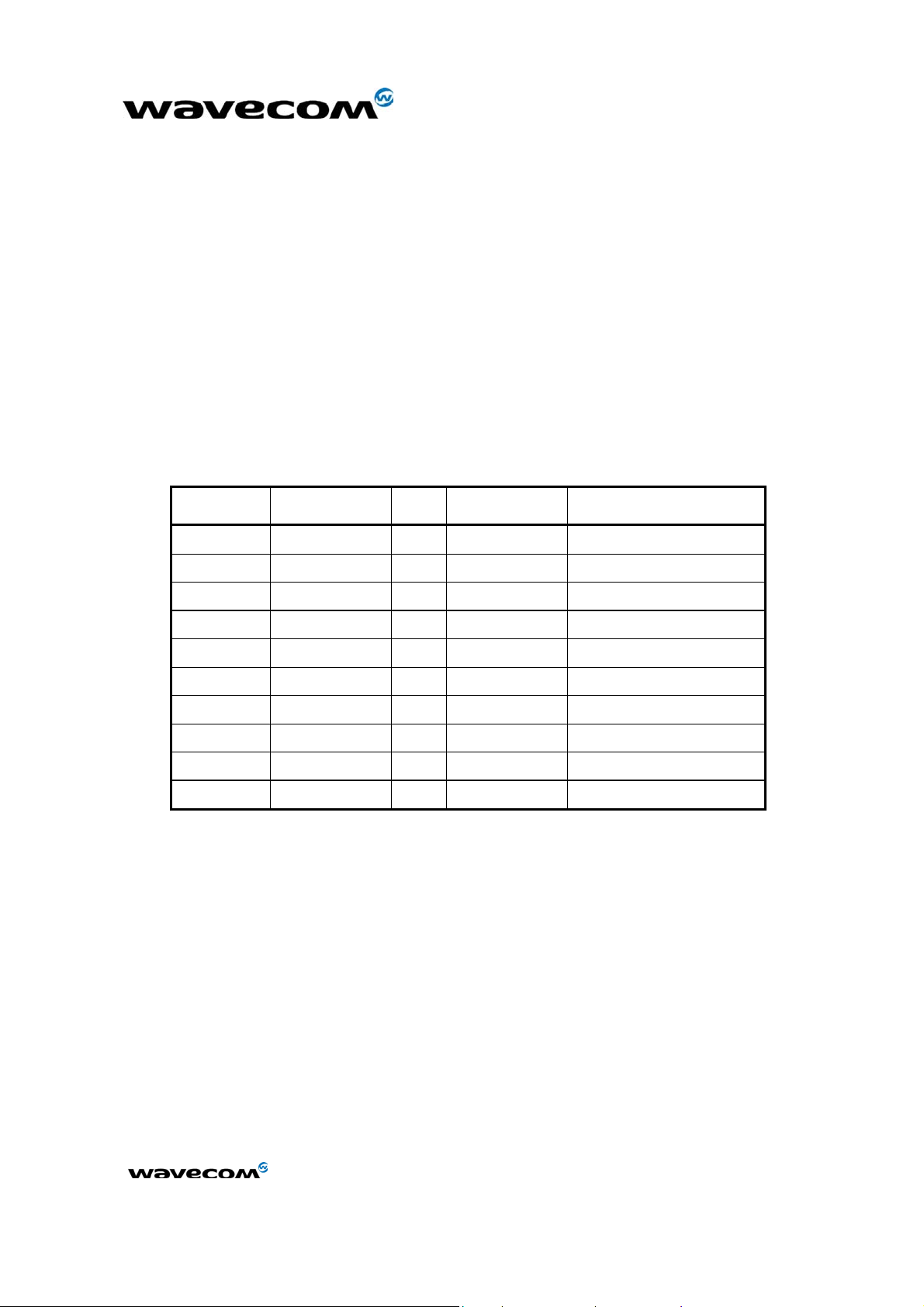
3.1 General Purpose Connector pin out description
Pin # Name I/O I/O type Description Comment
1 CHG_IN I Supply Supply for battery
charging
High current
2 CHG_IN I Supply Supply for battery
High current
charging
3 SIM_CLK O 2 X Clock for SIM interface
4 CHG_IN I Supply Supply for battery
High current
charging
5 SIM_RST O 2 X Reset for SIM interface
6 ON/~OFF I CMOS Power ON/OFF control
7 SIM_DATA I/O CMOS / 3X I/O for SIM interface
8 SDA/SPI_IO I/O CMOS/1X Wire interface or SPI
Serial Data
9 SIM_VCC O Supply SIM card supply 6 mA max
10 SCL/SPI_CLK O 1X Wire interface or SPI
Serial clock
11 VDD I Supply Low power supply 3.1 V minimum or
connected to VBATT
12 BOOT I CMOS BOOT
Pull down through 1 KΩ
for Flash downloading
13 ROW0 I/O CMOS/1X Keyboard Row
14 ~RST I/O SCHMITT Module Reset Active low
15 ROW1 I/O CMOS/1X Keyboard Row
16 ~INTR I CMOS External interrupt
Active low. 100 KΩ
Pull-up inside
17 ROW2 I/O CMOS/1X Keyboard Row
18 GPI or
CT103/TXD2 *
confidential ©
This document is the sole and exclusive property of WAVECOM. Not to be distributed or divulged without prior written
agreement.
Ce document est la propriété exclusive de WAVECOM. Il ne peut être communiqué ou divulgué à des tiers sans son
autorisation préalable.
I CMOS or 3x General Purpose Input or
Aux.serial Link (UART2)
100K Pull-down inside -
Multiplexed
Page : 42 / 61
Page 43

WM_PRJ_Q2400_PTS_002 - 003
14th April 2003
Pin # Name I/O I/O type Description Comment
19 ROW3 I/O CMOS/1X Keyboard Row
20 GPO2 or
CT104/RXD2 *
O 1X or CMOS General Purpose Output or
Aux.serial Link (UART2)
Multiplexed
21 ROW4 I/O CMOS/1X Keyboard Row
22 GPO1 O 3X General Purpose Output
23 COL0 I/O CMOS/1X Keyboard Column
24 GPIO0 or
CT106/CTS2 *
I/O CMOS/2X or
CMOS
General Purpose I/O
or Aux. serial Link
Multiplexed
(UART2)
25 COL1 I/O CMOS/1X Keyboard Column
26 GPO0 or
SPI_AUX
O 3X or
1X
General Purpose Output or
SPI Aux
Or SIM 3 V / 5 V
Multiplexed
27 COL2 I/O CMOS/1X Keyboard Column
28 SPI_EN or GPO3 O 1X or
CMOS
SPI enable or General
Purpose Output
Multiplexed
29 COL3 I/O CMOS/1X Keyboard Column
30 CT105/RTS1 I CMOS Serial link interface
Request To Send
(UART1)
Pull up to VCC with
100 kΩ when not
used
31 COL4 I/O CMOS/1X Keyboard Column
32 CT104/RXD1 O 1X Serial link interface
Receive (UART1)
33 AUXV0 I Analog Auxiliary ADC input 0 Can be tied to GND if
not used
34 CT108-2/DTR1 I CMOS Serial link interface
Data Terminal Ready
(UART1)
35 GPIO5 or
CT105/RTS2 *
I/O CMOS / 2X or 2X General Purpose I/O
or Aux. serial Link
Pull up to VCC with
100 kΩ when not
used
Multiplexed
(UART2)
36 CT107/DSR1 O 1X Serial link interface
Data Set Ready
(UART1)
37 CT106/CTS1 O 1X Serial link interface
Clear To Send
(UART1)
38 BAT_TEMP I Analog ADC input for battery
temperature measurement
39 CT103/TXD1 I CMOS Serial link interface
Transmit
Can be tied to GND if
not used
Pull up to VCC with
100 kΩ when not
confidential ©
This document is the sole and exclusive property of WAVECOM. Not to be distributed or divulged without prior written
agreement.
Ce document est la propriété exclusive de WAVECOM. Il ne peut être communiqué ou divulgué à des tiers sans son
autorisation préalable.
Page : 43 / 61
Page 44

WM_PRJ_Q2400_PTS_002 - 003
14th April 2003
Pin # Name I/O I/O type Description Comment
(UART1) used
40 VCC O Supply 2.8 V digital supply output 10 mA max.
41 SPK1P O Analog Speaker 1
positive output
42 MIC1P I Analog Microphone 1 positive
input
43 SPK1N O Analog Speaker 1
negative output
44 MIC1N I Analog Microphone 1
negative input
45 SPK2P O Analog Speaker 2
positive output
46 MIC2P I Analog Microphone 2
positive input
47 SPK2N O Analog Speaker 2
negative output
48 MIC2N I Analog Microphone 2
negative input
49 BUZ O Analog Buzzer output 80 mA max
50 SIM_PRES I CMOS SIM Card Detect
51 GPIO3 or
I/O
CMOS/2X General Purpose I/O
Multiplexed
CT109/DCD1
O
Serial interface
Data Carrier Detect
(UART1)
52 GPIO1
FLASH LED
I/O CMOS/2X General Purpose I/O
Module State
Multiplexed
53 GPIO4 I/O CMOS/2X General Purpose I/O
54 GPIO2 or
CT125 / RI1
I/O
O
CMOS/2X General Purpose I/O
Serial interface
Multiplexed
Ring Indicator
(UART1)
55 +VBATT Supply Battery Input High current
56 VCC_RTC I/O Supply RTC back-up supply
57 +VBATT Supply Battery Input High current
58 +VBATT Supply Battery Input High current
59 +VBATT Supply Battery Input High current
60 +VBATT Supply Battery Input High current
* Auxiliary Serial link not available on Q24x6D and Q24x6E products
confidential ©
This document is the sole and exclusive property of WAVECOM. Not to be distributed or divulged without prior written
agreement.
Ce document est la propriété exclusive de WAVECOM. Il ne peut être communiqué ou divulgué à des tiers sans son
autorisation préalable.
Page : 44 / 61
Page 45

WM_PRJ_Q2400_PTS_002 - 003
14th April 2003
2
1
59
60
Figure 10: WISMO Quik Q24x6 sub-series pin position (bottom view)
confidential ©
This document is the sole and exclusive property of WAVECOM. Not to be distributed or divulged without prior written
agreement.
Ce document est la propriété exclusive de WAVECOM. Il ne peut être communiqué ou divulgué à des tiers sans son
autorisation préalable.
Page : 45 / 61
Page 46

WM_PRJ_Q2400_PTS_002 - 003
14th April 2003
3.2 Environmental Specifications
Conditions Temperature range
Operating / Full GSM specifications compliant -20 °C to +55 °C
Storage -30 °C to +85 °C
ENVIRONMENTAL CLASSES
TYPE OF TEST STANDARDS STORAGE TRANSPORTATION OPERATING (PORT USE)
Class 1.2 Class 2.3 Class 7.3
Cold IEC 68-2.1 -25° C 72 h -40° C 72 h -20° C (GSM900) 16 h
Dry heat IEC 68-2.2 +70° C 72 h +70° C 72 h +55° C 16 h
Change of temperature IEC 68-2.14 -40° / +30° C 5 cycles -20° / +30° C (GSM900) 3 cycles
Damp heat IEC 68-2.30 +30° C 2 cycles +40° C 2 cycles +40° C 2 cycles
cyclic Db test 90% - 100% RH 90% - 100% RH 90% - 100% RH
Damp heat IEC 68-2.56 +30° C 4 days +40° C 4 days +40° C 4 days
Sinusoidal vibration IEC 68-2.6 5 - 62 Hz : 5 mm / s
Random vibration IEC 68-3.36 20 - 500Hz : - 3 dB / oct 12 - 150Hz : - 3 dB / oct
wide band Fdb test 3 x 10 min 3 x 30 min
Ab test -10° C (GSM1800/1900) 16h
Bb test
Na/Nb test t1 = 3 h -10° / +30° C (GSM1800/1900):
3 cycles t1 = 3 h
variant 1 variant 1 variant 1
Cb test
Fc test 62 - 200Hz : 2 m / s2
3 x 5 sweep cycles
5 - 20 Hz : 0.96 m2 / s3 10 -12 Hz : 0.96 m2 / s3
Electro-Static Discharge (ESD)
:
According to the norm EN 61000-4-2, the maximum ESD level supported by the Q24x6 sub-series is
±4 kV for all the pins including the antenna connector.
Humidity
:
According to IPC/JEDEC J-STD-033, the moisture class of the Q2400 series is level 3. The floor life
from the opening of the sealed bag is 168 hours.
Reflow soldering
:
The WISMO Quik Q2400 series does not support any reflow soldering.
confidential ©
This document is the sole and exclusive property of WAVECOM. Not to be distributed or divulged without prior written
agreement.
Ce document est la propriété exclusive de WAVECOM. Il ne peut être communiqué ou divulgué à des tiers sans son
autorisation préalable.
Page : 46 / 61
Page 47

WM_PRJ_Q2400_PTS_002 - 003
3.3 Mechanical specifications
3.3.1 Physical characteristics
The WISMO Quik Q24x6 Series module has a complete self-contained shield.
• Dimensions : 58.4 x 32.2 x 3.9 mm external dimensions (except shielding pins)
• Weight : <11 g
3.3.2 Mechanical drawings
The next page gives the mechanical specifications of WISMO Quik Q24x6 sub-series.
14th April 2003
confidential ©
This document is the sole and exclusive property of WAVECOM. Not to be distributed or divulged without prior written
agreement.
Ce document est la propriété exclusive de WAVECOM. Il ne peut être communiqué ou divulgué à des tiers sans son
autorisation préalable.
Page : 47 / 61
Page 48

WM_PRJ_Q2400_PTS_002 - 003
14th April 2003
Insert here mechanical drawing
confidential ©
This document is the sole and exclusive property of WAVECOM. Not to be distributed or divulged without prior written
agreement.
Ce document est la propriété exclusive de WAVECOM. Il ne peut être communiqué ou divulgué à des tiers sans son
autorisation préalable.
Page : 48 / 61
Page 49

WM_PRJ_Q2400_PTS_002 - 003
(
14th April 2003
4 Appendix
4.1 Wavecom acceptance test
The WISMO Quik Q24x6 sub-series complies with Wavecom standard acceptance test plan (Refer
to document [4]).
4.2 GSM Standard and Recommendations
The WISMO Quik Q24x6 sub-series is compliant with the following GSM ETSI, 3GPP, GCF and
NAPRD03 recommendations for Phase II.
Specification Reference Title
3GPP TS 45.005 v5.5.0 (2002-08)
Release 5
GSM 02.07 V8.0.0 (1999-07)
Technical Specification Group GSM/EDGE. Radio Access Network;
Radio transmission and reception
Digital cellular telecommunications system (Phase 2+);
Mobile Stations (MS) features (GSM 02.07 version 8.0.0 Release
1999)
GSM 02.60 V8.1.0 (1999-07)
Digital cellular telecommunications system (Phase 2+);
General Packet Radio Service (GPRS); Service description, Stage 1
(GSM 02.60 version 8.1.0 Release 1999)
GSM 03.60 V7.9.0 (2002-09) Technical Specification Group Services and System Aspects;
Digital cellular telecommunications system (Phase 2+); General
Packet Radio Service (GPRS); Service description; Stage 2 (Release
1998)
3GPP TS 43.064 V5.0.0 (2002-04) Technical Specification Group GERAN; Digital cellular
telecommunications system (Phase 2+); General Packet Radio
Service (GPRS); Overall description of the GPRS radio interface;
Stage 2 (Release 5)
3GPP TS 03.22 V8.7.0 (2002-08) Technical Specification Group GSM/EDGE. Radio Access Network;
Functions related to Mobile Station (MS) in idle mode and group
receive mode; (Release 1999)
3GPP TS 03.40 V7.5.0 (2001-12) Technical Specification Group Terminals;
Technical realization of the Short Message Service (SMS)
(Release 1998)
3GPP TS 03.41 V7.4.0 (2000-09) Technical Specification Group Terminals; Technical realization of Cell
Broadcast Service (CBS) (Release 1998)
ETSI EN 300 903 V8.1.1 (2000-11) Digital cellular telecommunications system (Phase 2+);
Transmission planning aspects of the speech service in the GSM
Public Land Mobile Network
confidential ©
This document is the sole and exclusive property of WAVECOM. Not to be distributed or divulged without prior written
agreement.
Ce document est la propriété exclusive de WAVECOM. Il ne peut être communiqué ou divulgué à des tiers sans son
autorisation préalable.
PLMN) system (GSM 03.50 version
Page : 49 / 61
Page 50

WM_PRJ_Q2400_PTS_002 - 003
q
14th April 2003
Specification Reference Title
8.1.1 Release 1999)
3GPP TS 04.06 V8.2.1 (2002-05) Technical Specification Group GSM/EDGE Radio Access Network;
Mobile Station - Base Station System (MS - BSS) interface; Data Link
(DL) layer specification (Release 1999)
3GPP TS 04.08 V7.18.0 (2002-09) Technical Specification Group Core Network;
Digital cellular telecommunications system (Phase 2+);
Mobile radio interface layer 3 specification (Release 1998)
3GPP TS 04.10 V7.1.0 (2001-12) Technical Specification Group Core Networks;
Mobile radio interface layer 3 Supplementary services specification;
General aspects (Release 1998)
3GPP TS 04.11 V7.1.0 (2000-09) Technical Specification Group Core Network; Digital cellular
telecommunications system (Phase 2+); Point-to-Point (PP) Short
Message Service (SMS) support on mobile radio interface
(Release 1998)
3GPP TS 45.005 v5.5.0 (2002-08) Technical Specification Group GSM/EDGE. Radio Access Network;
Radio transmission and reception (Release 5)
3GPP TS 45.008 V5.8.0 (2002-08) Technical Specification Group GSM/EDGE
Radio Access Network; Radio subsystem link control (Release 5)
3GPP TS 45.010 V5.1.0 (2002-08)
Technical Specification Group GSM/EDGE
Radio Access Network; Radio subsystem synchronization (Release 5)
3GPP TS 46.010 V5.0.0 (2002-06) Technical Specification Group Services and System Aspects;
Full rate speech; Transcoding (Release 5)
3GPP TS 46.011 V5.0.0 (2002-06) Technical Specification Group Services and System Aspects;
Full rate speech; Substitution and muting of lost frames for
full rate speech channels (Release 5)
3GPP TS 46.012 V5.0.0 (2002-06) Technical Specification Group Services and System Aspects;
Full rate speech; Comfort noise aspect for full rate speech traffic
channels (Release 5)
3GPP TS 46.031 V5.0.0 (2002-06) Technical Specification Group Services and System Aspects;
Full rate speech; Discontinuous Transmission (DTX) for full rate
speech traffic channels (Release 5)
3GPP TS 46.032 V5.0.0 (2002-06)
Technical Specification Group Services and System Aspects;
Full rate speech; Voice Activity Detector (VAD) for full rate speech
traffic channels (Release 5)
TS 100 913V8.0.0 (1999-08)
Digital cellular telecommunications system (Phase 2+);
General on Terminal Adaptation Functions (TAF) for Mobile Stations
(MS) (GSM 07.01 version 8.0.0 Release 1999)
GSM 09.07 V8.0.0 (1999-08)
This document is the sole and exclusive property of WAVECOM. Not to be distributed or divulged without prior written
agreement.
Ce document est la propriété exclusive de WAVECOM. Il ne peut être communiqué ou divulgué à des tiers sans son
autorisation préalable.
confidential ©
Digital cellular telecommunications system (Phase 2+);
General re
uirements on interworking between the Public Land Mobile
Page : 50 / 61
Page 51

WM_PRJ_Q2400_PTS_002 - 003
Specification Reference Title
Network (PLMN) and the Integrated Services Digital Network (ISDN)
or Public Switched Telephone Network (PSTN) (GSM 09.07 version
8.0.0 Release 1999)
14th April 2003
3GPP TS 51.010-1 v5.0.0 (2002-
09)
Technical Specification Group GSM/EDGE ; Radio Access
Network ;Digital cellular telecommunications system (Phase
2+);Mobile Station (MS) conformance specification; Part 1:
Conformance specification (Release 5)
3GPP TS 51.011 V5.0.0 (2001-
12)
ETS 300 641 (1998-03)
Technical Specification Group Terminals; Specification of the
Subscriber Identity Module - Mobile Equipment (SIM - ME) interface
(Release 5)
Digital cellular telecommunications system (Phase 2);
Specification of the 3 Volt Subscriber Identity Module - Mobile
Equipment (SIM-ME) interface (GSM 11.12 version 4.3.1)
GCF-CC V3.7.1 (2002-08) Global Certification Forum – Certification criteria
NAPRD03 V2.6.0 (2002-06) North America Permanent Reference Document for PTCRB tests
confidential ©
This document is the sole and exclusive property of WAVECOM. Not to be distributed or divulged without prior written
agreement.
Ce document est la propriété exclusive de WAVECOM. Il ne peut être communiqué ou divulgué à des tiers sans son
autorisation préalable.
Page : 51 / 61
Page 52

WM_PRJ_Q2400_PTS_002 - 003
14th April 2003
4.3 Safety recommendations (for information only)
IMPORTANT
FOR THE EFFICIENT AND SAFE OPERATION OF
YOUR GSM APPLICATION BASED ON WISMO Quik Q24x6 Series
PLEASE READ THIS INFORMATION CAREFULLY
4.3.1 RF safety
4.3.1.1 General
Your GSM terminal
spread all over the world. It covers Europe, Asia and some parts of America and Africa. This is the
most used telecommunication standard.
Your GSM terminal is actually a low power radio transmitter and receiver. It sends out and receives
radio frequency energy. When you use your GSM application, the cellular system which handles
your calls controls both the radio frequency and the power level of your cellular modem.
3
is based on the GSM standard for cellular technology. The GSM standard is
4.3.1.2 Exposure to RF energy
There has been some public concern about possible health effects of using GSM terminals.
Although research on health effects from RF energy has focused on the current RF technology for
many years, scientists have begun research regarding newer radio technologies, such as GSM.
After existing research had been reviewed, and after compliance to all applicable safety standards
had been tested, it has been concluded that the product was fitted for use.
If you are concerned about exposure to RF energy there are things you can do to minimize
exposure. Obviously, limiting the duration of your calls will reduce your exposure to RF energy. In
addition, you can reduce RF exposure by operating your cellular terminal efficiently by following the
below guidelines.
4.3.1.3 Efficient terminal operation
For your GSM terminal to operate at the lowest power level, consistent with satisfactory call quality:
• If your terminal has an extendible antenna, extend it fully. Some models allow you to place a
call with the antenna retracted. However your GSM terminal operates more efficiently with
the antenna fully extended.
• Do not hold the antenna when the terminal is « IN USE ». Holding the antenna affects call
quality and may cause the modem to operate at a higher power level than needed.
4.3.1.4 Modular Transmitter
Modular transmitter. This device is to be used only for mobile and fixed applications.
The antenna(s) used for this transmitter must be installed to provide a separation distance of
at least 20 cm from all persons and must not be co-located or operating in conjunction with
any other antenna or transmitter. The antenna(s) used for this transmitter must not exceed
3
based on WISMO2D
confidential ©
This document is the sole and exclusive property of WAVECOM. Not to be distributed or divulged without prior written
agreement.
Ce document est la propriété exclusive de WAVECOM. Il ne peut être communiqué ou divulgué à des tiers sans son
autorisation préalable.
Page : 52 / 61
Page 53

WM_PRJ_Q2400_PTS_002 - 003
14th April 2003
a gain of 3 dBi for mobile operation and 7 dBi for fixed operation. Users and OEM
integrators must be provided with antenna installation instructions and transmitter operating
conditions for satisfying RF exposure compliance. OEM must also be provided with
labelling instructions. This device contains 900 MHz GSM functions that are not operational
in U.S. Territories. This filing is only applicable for GSM 850 MHz and 1900 MHz PCS
operations.
4.3.1.5 Antenna care and replacement
Do not use the GSM terminal with a damaged antenna. If a damaged antenna comes into contact
with the skin, a minor burn may result. Replace a damaged antenna immediately. Consult your
manual to see if you may change the antenna yourself. If so, use only a manufacturer-approved
antenna. Otherwise, have your antenna repaired by a qualified technician.
Use only the supplied or approved antenna. Unauthorized antennas, modifications or attachments
could damage the terminal and may contravene local RF emission regulations or invalidate type
approval.
4.3.2 General safety
4.3.2.1 Driving
Check the laws and the regulations regarding the use of cellular devices in the area where you have
to drive as you always have to comply with them. When using your GSM terminal while driving,
please:
• give full attention to driving,
• pull off the road and park before making or answering a call if driving conditions so require.
4.3.2.2 Electronic devices
Most electronic equipment, for example in hospitals and motor vehicles, is shielded from RF energy.
However RF energy may affect some improperly shielded electronic equipment.
4.3.2.3 Vehicle electronic equipment
Check your vehicle manufacturer representative to determine if any on-board electronic equipment
is adequately shielded from RF energy.
4.3.2.4 Medical electronic equipment
Consult the manufacturer of any personal medical devices (such as pacemakers, hearing aids,
etc...) to determine if they are adequately shielded from external RF energy.
Turn your terminal OFF in health care facilities when any regulations posted in the area instruct you
to do so. Hospitals or health care facilities may be using RF monitoring equipment.
confidential ©
This document is the sole and exclusive property of WAVECOM. Not to be distributed or divulged without prior written
agreement.
Ce document est la propriété exclusive de WAVECOM. Il ne peut être communiqué ou divulgué à des tiers sans son
autorisation préalable.
Page : 53 / 61
Page 54

WM_PRJ_Q2400_PTS_002 - 003
14th April 2003
4.3.2.5 Aircraft
Turn your terminal OFF before boarding any aircraft.
Use it on the ground only with crew permission.
Do not use it in the air.
To prevent possible interference with aircraft systems, Federal Aviation Administration (FAA)
regulations require you to have permission from a crew member to use your terminal while the
aircraft is on the ground. To prevent interference with cellular systems, local RF regulations prohibit
using your modem while airborne.
4.3.2.6 Children
Do not allow children to play with your GSM terminal. It is not a toy. Children could hurt themselves
or others (by poking themselves or others in the eye with the antenna, for example). Children could
damage the modem, or make calls that increase your modem bills.
4.3.2.7 Blasting areas
To avoid interfering with blasting operations, turn your unit OFF when in a « blasting area » or in
areas posted: « turn off two-way radio ». Construction crew often use remote control RF devices to
set off explosives.
4.3.2.8 Potentially explosive atmospheres
Turn your terminal OFF when in any area with a potentially explosive atmosphere. It is rare, but your
modem or its accessories could generate sparks. Sparks in such areas could cause an explosion or
fire resulting in bodily injuries or even death.
Areas with a potentially explosive atmosphere are often, but not always, clearly marked. They
include fuelling areas such as petrol stations; below decks on boats; fuel or chemical transfer or
storage facilities; and areas where the air contains chemicals or particles, such as grain, dust, or
metal powders.
Do not transport or store flammable gas, liquid, or explosives, in the compartment of your vehicle
which contains your terminal or accessories.
Before using your terminal in a vehicle powered by liquefied petroleum gas (such as propane or
butane) ensure that the vehicle complies with the relevant fire and safety regulations of the country
in which the vehicle is to be used.
confidential ©
This document is the sole and exclusive property of WAVECOM. Not to be distributed or divulged without prior written
agreement.
Ce document est la propriété exclusive de WAVECOM. Il ne peut être communiqué ou divulgué à des tiers sans son
autorisation préalable.
Page : 54 / 61
Page 55

WM_PRJ_Q2400_PTS_002 - 003
14th April 2003
4.4 General Purpose Connector data sheet
The next 6 pages are the KYOCERA/ELCO data sheets for the GPC (also available from
http://www.avxcorp.com
.
confidential ©
This document is the sole and exclusive property of WAVECOM. Not to be distributed or divulged without prior written
agreement.
Ce document est la propriété exclusive de WAVECOM. Il ne peut être communiqué ou divulgué à des tiers sans son
autorisation préalable.
Page : 55 / 61
Page 56

AVX 1/6
WM_PRJ_Q2400_PTS_002 - 003
14th April 2003
confidential ©
This document is the sole and exclusive property of WAVECOM. Not to be distributed or divulged without prior written
agreement.
Ce document est la propriété exclusive de WAVECOM. Il ne peut être communiqué ou divulgué à des tiers sans son
autorisation préalable.
Page : 56 / 61
Page 57

AVX 2/6
WM_PRJ_Q2400_PTS_002 - 003
14th April 2003
confidential ©
This document is the sole and exclusive property of WAVECOM. Not to be distributed or divulged without prior written
agreement.
Ce document est la propriété exclusive de WAVECOM. Il ne peut être communiqué ou divulgué à des tiers sans son
autorisation préalable.
Page : 57 / 61
Page 58

AVX 3/6
WM_PRJ_Q2400_PTS_002 - 003
14th April 2003
confidential ©
This document is the sole and exclusive property of WAVECOM. Not to be distributed or divulged without prior written
agreement.
Ce document est la propriété exclusive de WAVECOM. Il ne peut être communiqué ou divulgué à des tiers sans son
autorisation préalable.
Page : 58 / 61
Page 59

AVX 4/6
WM_PRJ_Q2400_PTS_002 - 003
14th April 2003
confidential ©
This document is the sole and exclusive property of WAVECOM. Not to be distributed or divulged without prior written
agreement.
Ce document est la propriété exclusive de WAVECOM. Il ne peut être communiqué ou divulgué à des tiers sans son
autorisation préalable.
Page : 59 / 61
Page 60

AVX 5/6
WM_PRJ_Q2400_PTS_002 - 003
14th April 2003
confidential ©
This document is the sole and exclusive property of WAVECOM. Not to be distributed or divulged without prior written
agreement.
Ce document est la propriété exclusive de WAVECOM. Il ne peut être communiqué ou divulgué à des tiers sans son
autorisation préalable.
Page : 60 / 61
Page 61

AVX 6/6
WM_PRJ_Q2400_PTS_002 - 003
14th April 2003
confidential ©
This document is the sole and exclusive property of WAVECOM. Not to be distributed or divulged without prior written
agreement.
Ce document est la propriété exclusive de WAVECOM. Il ne peut être communiqué ou divulgué à des tiers sans son
autorisation préalable.
Page : 61 / 61
 Loading...