

Page 1
PCIE-100
User Guide
Reference: WM_DEV_PCIE-100_PTS_003
Revision: 001
Date: July, 01th 2008
This document is the sole and exclusive property of WAVECOM. Not to be distributed or divulged without prior written
confidential ©
agreement.
Ce document est la propriété exclusive de WAVECOM. Il ne peut être communiqué ou divulgué à des tiers sans son
autorisation préalable.
Page : 1 / 37
Page 2

PRELIMINARY
WM_DEV_PCIE100_PTS_003
July, 01th 2008
Document Information
Level Date History of the evolution
001 01/07/2008 Creation (Preliminary version) EMH
This document is the sole and exclusive property of WAVECOM. Not to be distributed or divulged without prior written
confidential ©
agreement.
Ce document est la propriété exclusive de WAVECOM. Il ne peut être communiqué ou divulgué à des tiers sans son
autorisation préalable.
Page : 2 / 37
Page 3

PRELIMINARY
Overview
This document defines and specifies the PCIE-100 Wavecom product.
WM_DEV_PCIE100_PTS_003
July, 01th 2008
This document is the sole and exclusive property of WAVECOM. Not to be distributed or divulged without prior written
confidential ©
agreement.
Ce document est la propriété exclusive de WAVECOM. Il ne peut être communiqué ou divulgué à des tiers sans son
autorisation préalable.
Page : 3 / 37
Page 4

PRELIMINARY
Contents
WM_DEV_PCIE100_PTS_003
July, 01th 2008
Document Information.................................................................................................................2
Overview .................................................................................................................................... 3
Contents .....................................................................................................................................4
Cautions ..................................................................................................................................... 7
Trademarks.................................................................................................................................7
Copyright ....................................................................................................................................7
1
References ...................................................................................................................... 8
1.1
References documents.....................................................................................................8
1.1.1
WAVECOM reference document ..............................................................................8
1.1.2
General reference document ................................................................................... 8
1.2
List of abbreviations ........................................................................................................ 9
2
Interfaces ..................................................................................................................... 11
2.1
Mini-PCI Pin Out ............................................................................................................ 11
2.2
Not Connected Pins ....................................................................................................... 12
2.3
Power supply ................................................................................................................ 13
2.3.1
Electrical Characteristics ....................................................................................... 13
2.3.2
Pin description ..................................................................................................... 13
2.3.3
Application........................................................................................................... 13
2.3.4
Power consumption .............................................................................................. 13
2.3.4.1
2.3.4.2
2.3.4.3
2.3.4.4
2.3.4.5
2.4
2.4.1
2.4.2
2.4.3
2.5
2.5.1
2.5.2
This document is the sole and exclusive property of WAVECOM. Not to be distributed or divulged without prior written
agreement.
Ce document est la propriété exclusive de WAVECOM. Il ne peut être communiqué ou divulgué à des tiers sans son
autorisation préalable.
Idle Mode power consumption ....................................................................... 14
GSM power consumption ............................................................................... 14
GPRS power consumption .............................................................................. 14
EGPRS power consumption ............................................................................ 16
UMTS power consumption ............................................................................. 17
SIM Interface ................................................................................................................ 18
Features .............................................................................................................. 18
Pin description ..................................................................................................... 19
Application........................................................................................................... 19
Reset signals ................................................................................................................. 20
Features .............................................................................................................. 20
Pin description ..................................................................................................... 21
confidential ©
Page : 4 / 37
Page 5

2.6
2.7
2.8
3
3.1
3.2
PRELIMINARY
2.5.3
Application........................................................................................................... 21
FLASH-LED signal .......................................................................................................... 22
2.6.1
Features .............................................................................................................. 22
2.6.2
Pin description ..................................................................................................... 22
2.6.3
Application........................................................................................................... 22
USB 2.0 interface........................................................................................................... 23
2.7.1
Features .............................................................................................................. 23
2.7.2
Pin description ..................................................................................................... 23
2.7.3
Application........................................................................................................... 24
RF interface .................................................................................................................. 25
2.8.1
RF connection ...................................................................................................... 25
2.8.2
RF performances .................................................................................................. 26
Environmental Specifications .......................................................................................... 27
Temperature Range....................................................................................................... 27
Mechanical specifications ............................................................................................... 27
3.2.1
Mechanical drawings ............................................................................................ 27
WM_DEV_PCIE100_PTS_003
July, 01th 2008
3.3
Thermal specifications ................................................................................................... 28
4
Peripheral devices references ......................................................................................... 29
4.1
Mini-PCI Connector........................................................................................................ 29
4.2
Mini-PCI Latch Up.......................................................................................................... 29
4.3
SIM Card Reader ........................................................................................................... 29
4.4
Antenna Connector ........................................................................................................ 29
4.5
GSM antenna ................................................................................................................ 29
5
Noises and design.......................................................................................................... 30
5.1
EMC recommendations .................................................................................................. 30
5.2
Power Supply ................................................................................................................ 30
6
Appendix....................................................................................................................... 31
6.1
Standards and Recommendations................................................................................... 31
6.2
Safety recommendations (for information only) ............................................................... 34
6.2.1
RF safety ............................................................................................................. 34
6.2.1.1
6.2.1.2
6.2.1.3
6.2.1.4
6.2.2
6.2.2.1
6.2.2.2
6.2.2.3
6.2.2.4
This document is the sole and exclusive property of WAVECOM. Not to be distributed or divulged without prior written
agreement.
Ce document est la propriété exclusive de WAVECOM. Il ne peut être communiqué ou divulgué à des tiers sans son
autorisation préalable.
General ........................................................................................................ 34
Exposure to RF energy .................................................................................. 34
Efficient terminal operation ............................................................................ 34
Antenna care and replacement....................................................................... 34
General safety...................................................................................................... 35
Driving ......................................................................................................... 35
Electronic devices.......................................................................................... 35
Vehicle electronic equipment.......................................................................... 35
Medical electronic equipment ......................................................................... 35
confidential ©
Page : 5 / 37
Page 6

PRELIMINARY
6.2.2.5
6.2.2.6
6.2.2.7
6.2.2.8
Aircraft ......................................................................................................... 35
Children........................................................................................................ 35
Blasting areas ............................................................................................... 36
Potentially explosive atmospheres .................................................................. 36
WM_DEV_PCIE100_PTS_003
July, 01th 2008
This document is the sole and exclusive property of WAVECOM. Not to be distributed or divulged without prior written
confidential ©
agreement.
Ce document est la propriété exclusive de WAVECOM. Il ne peut être communiqué ou divulgué à des tiers sans son
autorisation préalable.
Page : 6 / 37
Page 7
PRELIMINARY
WM_DEV_PCIE100_PTS_003
July, 01th 2008
Cautions
This platform contains a modular transmitter. This device is used for wireless applications. Note that
all electronics parts and elements are ESD sensitive.
Information provided herein by WAVECOM is accurate and reliable. However no responsibility is
assumed for its use and any of such WAVECOM information is herein provided “as is” without any
warranty of any kind, whether express or implied.
General information about WAVECOM and its range of products is available at the following internet
address: http://www.wavecom.com
Trademarks
®, WAVECOM®, WISMO®, Open AT® and certain other trademarks and logos appearing on this
document, are filed or registered trademarks of Wavecom S.A. in France or in other countries. All
other company and/or product names mentioned may be filed or registered trademarks of their
respective owners.
Copyright
This manual is copyrighted by WAVECOM with all rights reserved. No part of this manual may be
reproduced in any form without the prior written permission of WAVECOM. No patent liability is
assumed with respect to the use of their respective owners.
This document is the sole and exclusive property of WAVECOM. Not to be distributed or divulged without prior written
confidential ©
agreement.
Ce document est la propriété exclusive de WAVECOM. Il ne peut être communiqué ou divulgué à des tiers sans son
autorisation préalable.
Page : 7 / 37
Page 8

PRELIMINARY
WM_DEV_PCIE100_PTS_003
July, 01th 2008
1 References
1.1 References documents
For more details, several references documents can be consulted. The WAVECOM reference
documents are provided in the WAVECOM documents package contrary at the general reference
documents which are not WAVECOM owner.
1.1.1 WAVECOM reference document
1.1.2 General reference document
[1] PCI EXPRESS MINI CARD ELECTROMECHANICAL SPECIFICATION, REV 1.2
[2] USB2.0 standard
This document is the sole and exclusive property of WAVECOM. Not to be distributed or divulged without prior written
confidential ©
agreement.
Ce document est la propriété exclusive de WAVECOM. Il ne peut être communiqué ou divulgué à des tiers sans son
autorisation préalable.
Page : 8 / 37
Page 9

PRELIMINARY
1.2 List of abbreviations
Abbreviation Definition
AC Alternative Current
AT ATtention (prefix for modem commands)
CLK CLocK
CMOS Complementary Metal Oxide Semiconductor
CS Coding Scheme
dB Decibel
DCS Digital Cellular System
E-GSM Extended GSM
EMC ElectroMagnetic Compatibility
EMI ElectroMagnetic Interference
WM_DEV_PCIE100_PTS_003
July, 01th 2008
ESD ElectroStatic Discharges
FTA Full Type Approval
GND GrouND
GPIO General Purpose Input Output
GPRS General Packet Radio Service
GSM Global System for Mobile communications
LED Light Emitting Diode
na Not Applicable
NOM NOMinal
NTC Négative Temperature Coefficient
PCB Printed Circuit Board
RF Radio Frequency
RST ReSeT
RX Receive
SIM Subscriber Identification Module
SPI Serial Peripheral Interface
SPL Sound Pressure Level
SPK SPeaKer
TBC To Be Confirmed
TDMA Time Division Multiple Access
TP Test Point
This document is the sole and exclusive property of WAVECOM. Not to be distributed or divulged without prior written
confidential ©
agreement.
Ce document est la propriété exclusive de WAVECOM. Il ne peut être communiqué ou divulgué à des tiers sans son
autorisation préalable.
Page : 9 / 37
Page 10

PRELIMINARY
Abbreviation Definition
TX Transmit
TYP TYPical
USB Universal Serial Bus
VSWR Voltage Standing Wave Ratio
.
WM_DEV_PCIE100_PTS_003
July, 01th 2008
This document is the sole and exclusive property of WAVECOM. Not to be distributed or divulged without prior written
confidential ©
agreement.
Ce document est la propriété exclusive de WAVECOM. Il ne peut être communiqué ou divulgué à des tiers sans son
autorisation préalable.
Page : 10 / 37
Page 11
PRELIMINARY
WM_DEV_PCIE100_PTS_003
2 Interfaces
2.1 Mini-PCI Pin Out
Pin Number Pin Name Description I/O Voltage Domain
1 NC NC N/A N/A
2 VBATT Power Supply I 3.3V
3 NC NC N/A N/A
4 GND Power Supply I GND
5 NC NC N/A N/A
6 NC NC N/A N/A
7 NC NC N/A N/A
8 SIM_POWER SIM O 1V8 / 2V9
9 GND Power Supply I GND
10 SIM_DATA SIM I/O 1V8 / 2V9
11 NC NC N/A N/A
12 SIM_CLK SIM O 1V8 / 2V9
13 NC NC N/A N/A
14 SIM_RESET SIM O 1V8 / 2V9
15 GND Power Supply I GND
16 NC NC N/A N/A
17 NC NC N/A N/A
18 GND Power Supply I GND
19 NC NC N/A N/A
20 NC NC N/A N/A
21 GND Power Supply I GND
22 RESET RESET I 3.3V
23 NC NC N/A N/A
24 NC NC N/A N/A
25 NC NC N/A N/A
26 GND Power Supply I GND
27 GND Power Supply I GND
28 NC NC N/A N/A
29 GND Power Supply I GND
30 NC NC N/A N/A
July, 01th 2008
This document is the sole and exclusive property of WAVECOM. Not to be distributed or divulged without prior written
confidential ©
agreement.
Ce document est la propriété exclusive de WAVECOM. Il ne peut être communiqué ou divulgué à des tiers sans son
autorisation préalable.
Page : 11 / 37
Page 12
PRELIMINARY
WM_DEV_PCIE100_PTS_003
31 NC NC N/A N/A
32 NC NC N/A N/A
33 NC NC N/A N/A
34 GND Power Supply I GND
35 GND Power Supply I GND
36 USB_D- USB I/O 3.3V
37 NC NC N/A N/A
38 USB_D+ USB I/O 3.3V
39 VBATT Power Supply I 3.3V
40 NC NC N/A N/A
41 VBATT Power Supply I 3.3V
42 FLASH_LED Status O Open Drain
43 GND Power Supply I GND
44 NC NC N/A N/A
45 NC NC N/A N/A
46 NC NC N/A N/A
47 NC NC N/A N/A
48 NC NC N/A N/A
49 NC NC N/A N/A
50 GND Power Supply I GND
51 NC NC N/A N/A
52 VBATT Power Supply I 3.3V
July, 01th 2008
2.2 Not Connected Pins
Not connected pins are expected to be not terminated on either the add-in card or system board
side of the connector. These pins are reserved for definition with future revisions of this
specification.
Non-standard use of these pins may result in incompatibilities in solutions aligned with the future
revision.
This document is the sole and exclusive property of WAVECOM. Not to be distributed or divulged without prior written
confidential ©
agreement.
Ce document est la propriété exclusive de WAVECOM. Il ne peut être communiqué ou divulgué à des tiers sans son
autorisation préalable.
Page : 12 / 37
Page 13
2.3 Power supply
2.3.1 Electrical Characteristics
Input power Supply Voltage
PRELIMINARY
WM_DEV_PCIE100_PTS_003
July, 01th 2008
V
VBATT
V
MIN
V
NOM
I
MAX
Ripple max (U
MAX
3.0 3.3 3.6 (TBD)
ripp
)
2.3.2 Pin description
Signal Pin number
VBATT
2, 39, 41, 52
2.3.3 Application
The power supply is one of the key issues in the design of a PCI Extreme product. The PCIE-100 is
supplied by one single power supply VBATT.
Due to the bursted emission in GSM / GPRS, the power supply must be able to deliver high current
peaks in a short time.
When designing the power supply for your application please pay specific attention to power losses.
Ensure that the input voltage VBATT never drops below specification. Any voltage drops that may
occur in a transmit burst should not exceed XXX mV.
The best approach to reducing voltage drops is to use a board-to-board connection as
recommended, and a low impedance power source. The resistance of the power supply lines on the
host board and of a battery pack should also be considered.
2.3.4 Power consumption
Power consumption is dependent on the configuration used. It is for this reason that the following
consumption values are given for each mode, RF band and type of wireless feature needed (GSM,
GPRS, EDGE and UMTS)
All the following information is given assuming a 50 Ω RF output.
The following consumption values were obtained by performing measurements on PCIE-100
samples at a temperature of 25° C.
Three VBATT values are used to measure the consumption, VBATT
VBATT
(3.3V).
TYP
(3.0V), VBATT
MIN
(3.6V) and
MAX
The average current is given for the three VBATT values.
This document is the sole and exclusive property of WAVECOM. Not to be distributed or divulged without prior written
confidential ©
agreement.
Ce document est la propriété exclusive de WAVECOM. Il ne peut être communiqué ou divulgué à des tiers sans son
autorisation préalable.
Page : 13 / 37
Page 14

PRELIMINARY
2.3.4.1 Idle Mode power consumption
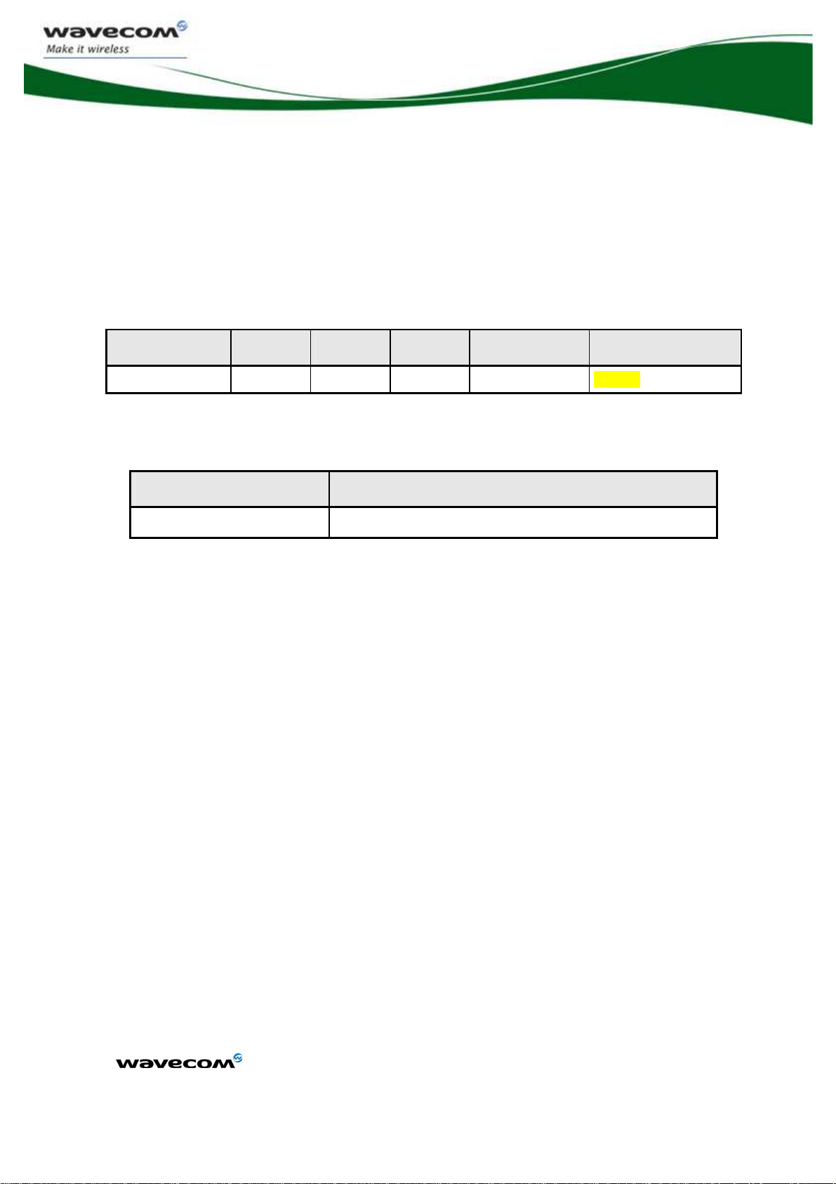
Operating mode Parameters
Idle Mode 62 mA
2.3.4.2 GSM power consumption
Operating mode Parameters
I
MIN
average
VBATT=3.6V
I
MIN
average
VBATT=3.6V
WM_DEV_PCIE100_PTS_003
July, 01th 2008
I
I
NOM
average
VBATT=3,3V
I
NOM
average
VBATT=3,3V
VBATT=3,2V
VBATT=3,2V
MAX
average
I
MAX
average
unit
Unit
850 MHz
PCL5 (TX power 33dBm)
PCL19 (TX power 5dBm)
PCL5 (TX power 33dBm)
900 MHz
GSM
Connected Mode
1800 MHz
PCL19 (TX power 5dBm)
PCL0 (TX power 30dBm)
PCL15 (TX power 0dBm)
PCL0 (TX power 30dBm)
1900 MHz
PCL15 (TX power 0dBm)
2.3.4.3 GPRS power consumption
Operating mode Parameters
PCL5 (TX power 33dBm)
PCL19 (TX power 5dBm)
PCL5 (TX power 33dBm)
PCL19 (TX power 5dBm)
PCL0 (TX power 30dBm)
PCL15 (TX power 0dBm)
GPRS
(1Tx, 4Rx)
Connected Mode
850 MHz
900 MHz
1800 MHz
500 mA
200 mA
500 mA
200 mA
450 mA
200 mA
450 mA
200 mA
I
I
MIN
average
VBATT=3.6V
NOM
average
VBATT=3,3V
I
MAX
average
VBATT=3,2V
500 mA
200 mA
500 mA
200 mA
450 mA
200 mA
Unit
PCL0 (TX power 30dBm)
450 mA
1900 MHz
PCL15 (TX power 0dBm)
This document is the sole and exclusive property of WAVECOM. Not to be distributed or divulged without prior written
confidential ©
agreement.
Ce document est la propriété exclusive de WAVECOM. Il ne peut être communiqué ou divulgué à des tiers sans son
autorisation préalable.
200 mA
Page : 14 / 37
Page 15

PRELIMINARY
Operating mode Parameters
I
MIN
average
VBATT=3.6V
WM_DEV_PCIE100_PTS_003
July, 01th 2008
I
I
NOM
average
VBATT=3,3V
VBATT=3,2V
MAX
average
Unit
850 MHz
PCL5 (TX power 33dBm)
PCL19 (TX power 5dBm)
PCL5 (TX power 33dBm)
GPRS
900 MHz
PCL19 (TX power 5dBm)
(2Tx, 3Rx)
Connected Mode
1800 MHz
PCL0 (TX power 30dBm)
PCL15 (TX power 0dBm)
PCL0 (TX power 30dBm)
1900 MHz
PCL15 (TX power 0dBm)
Operating mode Parameters
850 MHz
PCL5 (TX power 33dBm)
PCL19 (TX power 5dBm)
PCL5 (TX power 33dBm)
GPRS
900 MHz
PCL19 (TX power 5dBm)
(4Tx, 4Rx)
Connected Mode
1800 MHz
PCL0 (TX power 30dBm)
PCL15 (TX power 0dBm)
690 mA
255 mA
620 mA
270 mA
550 mA
265 mA
550 mA
265 mA
I
I
MIN
average
VBATT=3.6V
NOM
average
VBATT=3,3V
I
MAX
average
VBATT=3,2V
940 mA
340 mA
780 mA
360 mA
750 mA
360 mA
Unit
PCL0 (TX power 30dBm)
750 mA
1900 MHz
PCL15 (TX power 0dBm)
360 mA
This document is the sole and exclusive property of WAVECOM. Not to be distributed or divulged without prior written
confidential ©
agreement.
Ce document est la propriété exclusive de WAVECOM. Il ne peut être communiqué ou divulgué à des tiers sans son
autorisation préalable.
Page : 15 / 37
Page 16

PRELIMINARY
2.3.4.4 EGPRS power consumption
Operating mode Parameters
I
MIN
average
VBATT=3.6V
WM_DEV_PCIE100_PTS_003
July, 01th 2008
I
I
NOM
average
VBATT=3,3V
VBATT=3,2V
MAX
average
Unit
850 MHz
PCL8 (TX power 27dBm)
PCL19 (TX power 5dBm)
EGPRS
MCS9
(1Tx, 4Rx)
Connected Mode
900 MHz
1800 MHz
PCL8 (TX power 27dBm)
PCL19 (TX power 5dBm)
PCL2 (TX power 26dBm)
PCL15 (TX power 0dBm)
PCL2 (TX power 26dBm)
1900 MHz
PCL15 (TX power 0dBm)
Operating mode Parameters
PCL8 (TX power 27dBm)
PCL19 (TX power 5dBm)
PCL8 (TX power 27dBm)
PCL19 (TX power 5dBm)
PCL2 (TX power 26dBm)
PCL15 (TX power 0dBm)
EGPRS
MCS9
(2Tx, 3Rx)
Connected Mode
850 MHz
900 MHz
1800 MHz
315 mA
215 mA
315 mA
215 mA
315 mA
215 mA
310 mA
215 mA
I
I
MIN
average
VBATT=3.6V
NOM
average
VBATT=3,3V
I
MAX
average
VBATT=3,2V
445 mA
285 mA
445 mA
285 mA
445 mA
285 mA
Unit
PCL2 (TX power 26dBm)
445 mA
1900 MHz
PCL15 (TX power 0dBm)
285 mA
This document is the sole and exclusive property of WAVECOM. Not to be distributed or divulged without prior written
confidential ©
agreement.
Ce document est la propriété exclusive de WAVECOM. Il ne peut être communiqué ou divulgué à des tiers sans son
autorisation préalable.
Page : 16 / 37
Page 17

PRELIMINARY
WM_DEV_PCIE100_PTS_003
July, 01th 2008
2.3.4.5 UMTS power consumption
Power consumption in WCDMA is fully linked to required output power of the PCIE-100. Here is
an evaluation of the consumption made in Band 1 on middle frequency.
Consumption versus Output power @ ARFCN 9750
900
850
800
750
700
650
600
550
I(mA)
500
450
400
350
300
250
200
-20 -18 -16 -14 -12 -10 -8 -6 -4 -2 0 2 4 6 8 10 12 14 16 18 20 22
Output power (dBm)
This document is the sole and exclusive property of WAVECOM. Not to be distributed or divulged without prior written
confidential ©
agreement.
Ce document est la propriété exclusive de WAVECOM. Il ne peut être communiqué ou divulgué à des tiers sans son
autorisation préalable.
Page : 17 / 37
Page 18

PRELIMINARY
WM_DEV_PCIE100_PTS_003
July, 01th 2008
2.4 SIM Interface
The Subscriber Identification Module can be directly connected to the PCIE-100 through this
dedicated interface.
The SIM interface controls a 3V / 1V8 SIM. This interface is fully compliant with GSM 11.11
recommendations concerning SIM functions.
2.4.1 Features
The SIM interface controls 1.8V and 3V SIM card.
Electrical Characteristics of SIM interface
Parameter Conditions Minimal Typical Maximal
SIM_DATA
Internal Pull Up SIM_DATA to SIM_VCC 6,5 10 14 kOhms
Input low voltage threshold 0.3 Volts
Input high voltage threshold VDD – 0.6 Volts
Input low current 1 mA
Input high current 20 µA
Output low voltage level 0.4 Volts
Output low voltage level 0.8 *
SIM_VCC
Capacitive load 30 pF
Rise / Fall Time 0,8 µs
SIM_CLK & SIM_RST
Digital output low level 0.4 Volts
Digital output high level
Capacitive load
SIM_CLK Rise / Fall Time 40 ns
0,8 *
SIM_VCC
30 pF
Volts
Volts
Unit
SIM_CLK Rise / Fall Time 100 ns
Output low voltage level 0.4 V
Output low voltage level 0.8 *
SIM_VCC
V
This document is the sole and exclusive property of WAVECOM. Not to be distributed or divulged without prior written
confidential ©
agreement.
Ce document est la propriété exclusive de WAVECOM. Il ne peut être communiqué ou divulgué à des tiers sans son
autorisation préalable.
Page : 18 / 37
Page 19

2.4.2 Pin description
PRELIMINARY
WM_DEV_PCIE100_PTS_003
July, 01th 2008
Signal Pin
SIM_CLK
SIM_RESET
SIM_DATA
SIM_POWER
2.4.3 Application
number
12
14
10
8
I/O I/O type Description
O 2V9 / 1V8 SIM Clock
O
I/O
O
2V9 / 1V8
2V9 / 1V8
2V9 / 1V8
SIM Reset
SIM Data
SIM Power Supply
The SIM interface controls 1.8V and 3V SIM card. It is recommended to add Transient Voltage
Suppressor diodes (TVS) on the signal connected to the SIM socket in order to prevent any
Electrostatics Discharge.
TVS diodes with low capacitance (less than 10 pF) have to be connected on SIM-CLK and SIM-DATA
signals to avoid any disturbance of the rising and falling edge.
These types of diodes are mandatory for the Full Type Approval. They shall be placed as close as
possible to the SIM socket.
The following references can be used: DALC208SC6 from ST Microelectronics.
This document is the sole and exclusive property of WAVECOM. Not to be distributed or divulged without prior written
confidential ©
agreement.
Ce document est la propriété exclusive de WAVECOM. Il ne peut être communiqué ou divulgué à des tiers sans son
autorisation préalable.
Page : 19 / 37
Page 20

PRELIMINARY
POWER ON SEQUENCE
3.3 V
RESET
RESET SEQUENCE
3.3 V
RESET
POWER OFF SEQUENCE
3.3 V
RESET
WM_DEV_PCIE100_PTS_003
July, 01th 2008
2.5 Reset signals
2.5.1 Features
Electrical Characteristics of the signals
Parameter Minimum Typ Maximum Unit
RESET
VIH
VIL
Input Capacitance
Output Capacitance
Input leakage current
Output Capacitance
2 3.6
-0.5 0.8
7
30
-10 10
-50 50
T_PVPGL
T_PERST
V
V
pF
pF
µA
µA
T_FAIL
RESET PIN ASSERTED
This document is the sole and exclusive property of WAVECOM. Not to be distributed or divulged without prior written
confidential ©
agreement.
Ce document est la propriété exclusive de WAVECOM. Il ne peut être communiqué ou divulgué à des tiers sans son
autorisation préalable.
Page : 20 / 37
Page 21
PRELIMINARY
WM_DEV_PCIE100_PTS_003
July, 01th 2008
Parameter Minimum Typ Maximum Unit
RESET
T_PVPGL
T_PERST
T_FAIL
TBD
TBD
TBD
ms
ms
ms
• T_PVPGL => RESET must remain active at least this long after power becomes valid
• T_PERST => When asserted, RESET must remain asserted at least this long
• T_FAIL => When power becomes invalid, RESET must be asserted within this time
2.5.2 Pin description
Signal Pin
I/O I/O type Description
number
RESET 22 I/O Open Drain* 3.3V PCIE-100 Reset
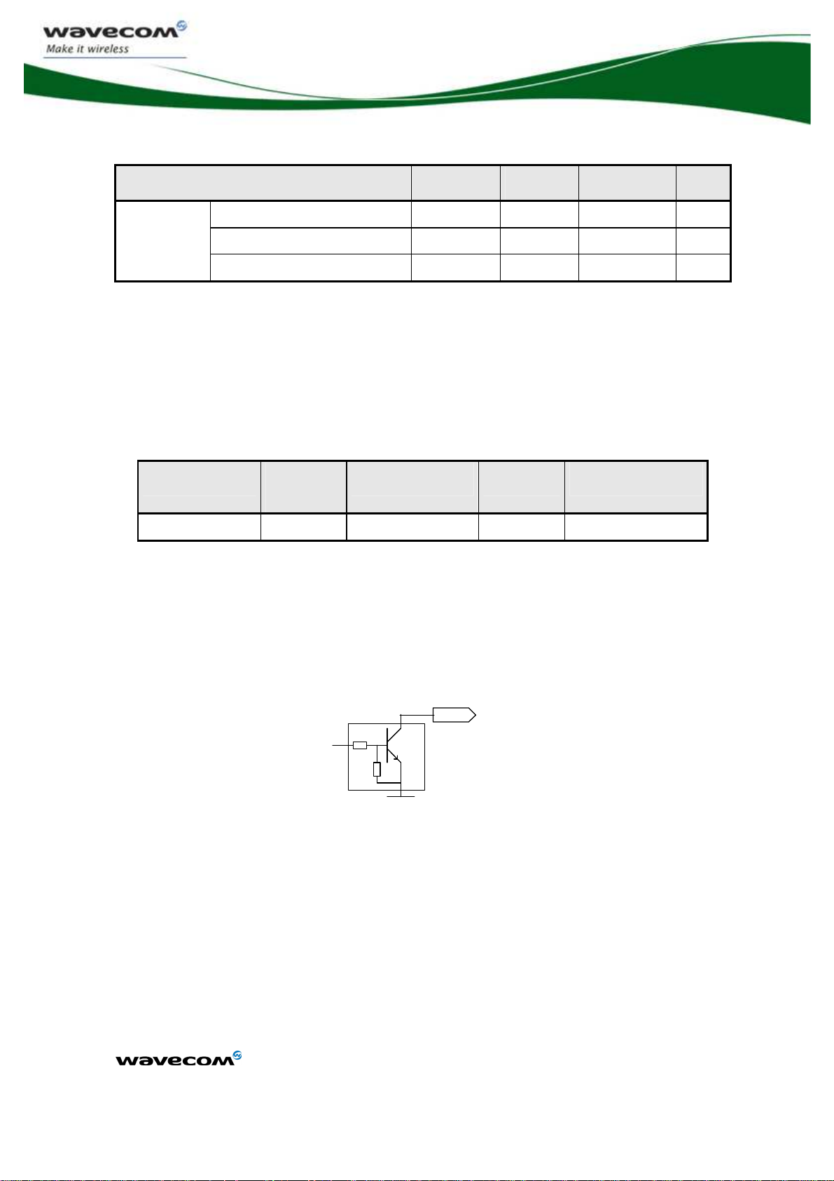
2.5.3 Application
The RESET signal is de-asserted to indicate when the system power sources are within their
specified voltage tolerance and are stable. RESET should be used to initialize the card functions
once power sources stabilize. RESET is asserted when power is switched off and also can be used
by the system to force a hardware reset on the card. The system may also use RESET to cause a
warm reset of the add-in card.
RESET
Reset
command
GND
T1
Rohm DTC144EE
Open collector or open drain transistor can be used. If an open collector is chosen, T1 can be a
Rohm DTC144EE.
This document is the sole and exclusive property of WAVECOM. Not to be distributed or divulged without prior written
confidential ©
agreement.
Ce document est la propriété exclusive de WAVECOM. Il ne peut être communiqué ou divulgué à des tiers sans son
autorisation préalable.
Page : 21 / 37
Page 22

PRELIMINARY
2.6 FLASH-LED signal
2.6.1 Features
FLASH-LED status
FLASH-LED status PCIE-100 status
LED OFF Radio is incapable of transmitting.
LED ON Radio is capable of transmitting.
Electrical characteristics of the signal
WM_DEV_PCIE100_PTS_003
July, 01th 2008
Parameter Condition Minimum Typ Maximum Unit
VOL 0.4 V
I
OUT
8 mA
2.6.2 Pin description
Signal Pin
I/O I/O type Reset state Description
number
FLASH-LED 42 O Open Drain Active Low
2.6.3 Application
« GSM »
FLA SH-LED
R1
47 0 Ω
1
2
D1
VBA TT
R1 value can be harmonized depending of the LED (D1) characteristics.
This document is the sole and exclusive property of WAVECOM. Not to be distributed or divulged without prior written
confidential ©
agreement.
Ce document est la propriété exclusive de WAVECOM. Il ne peut être communiqué ou divulgué à des tiers sans son
autorisation préalable.
Page : 22 / 37
Page 23

PRELIMINARY
WM_DEV_PCIE100_PTS_003
July, 01th 2008
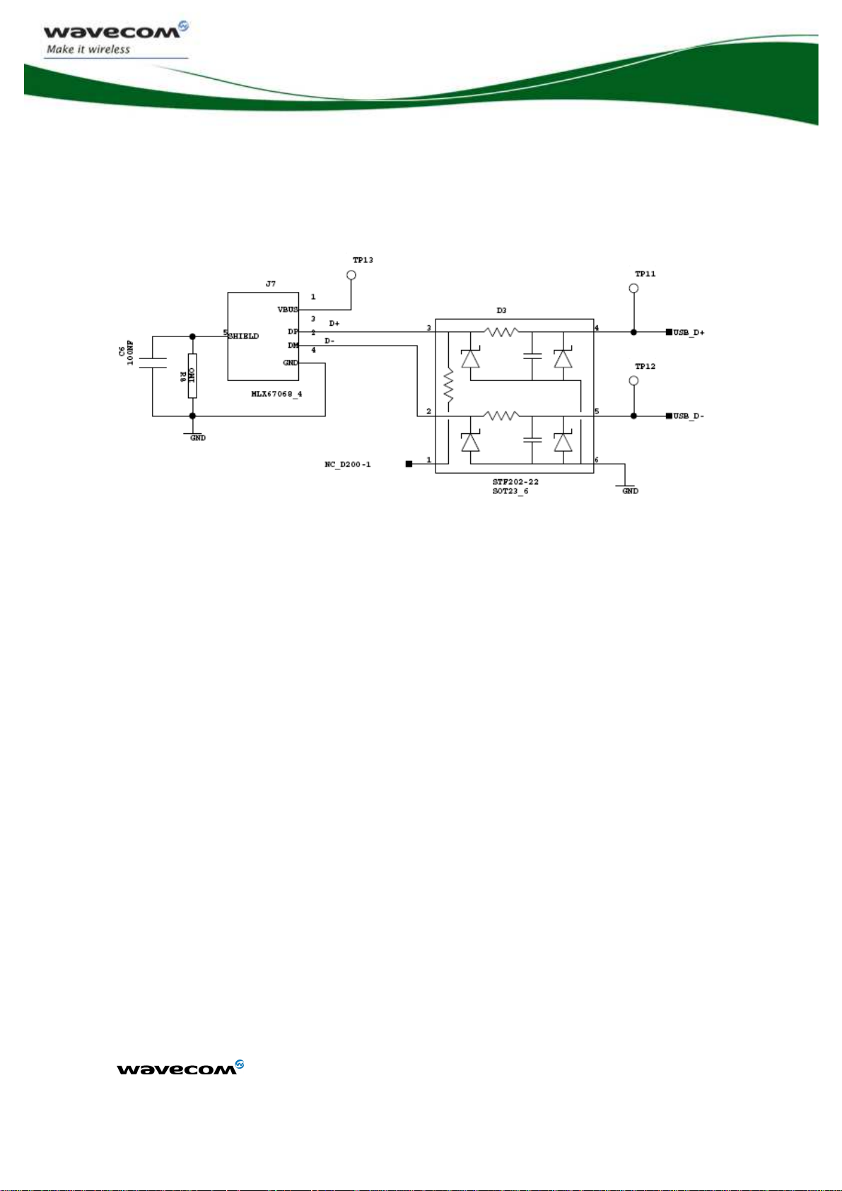
2.7 USB 2.0 interface
A 2-wire USB slave interface is available, compiling with USB 2.0 protocol signalling. The USB
interface signals are USB-DP, USB-DM and GND.
The USB interface supports USB 2.0 in all three modes (Low Speed, Full Speed, and High Speed).
Because there is not a separate USB-controlled voltage bus, USB functions implemented on a PCI
Express Mini Card add-in card are expected to report as self-powered devices. All enumeration, bus
protocol, and bus management features for this interface are defined by Universal Serial Bus
Specification, Revision 2.0.
2.7.1 Features
12Mbit/s full speed transfer rate
3.3V type compatible
USB Soft connect feature
Electrical characteristics of the signals
Parameter Min Typical Max Unit
USB_D-, USB_D+ 3 3.3 3.6 V
2.7.2 Pin description
Signal Pin
number
USB_D+
USB_D-
38
36
I/O I/O type Description
I/O USB
I/O USB
Differential data
interface positive
Differential data
interface negative
This document is the sole and exclusive property of WAVECOM. Not to be distributed or divulged without prior written
agreement.
Ce document est la propriété exclusive de WAVECOM. Il ne peut être communiqué ou divulgué à des tiers sans son
autorisation préalable.
confidential ©
Page : 23 / 37
Page 24
2.7.3 Application
PRELIMINARY
WM_DEV_PCIE100_PTS_003
July, 01th 2008
For USB interface, it is recommended to add EMI/RFI/ESD protection between PCIE-100 and USB
connector like shown on previous schematic. The following references can be used: STF2002-22
from SEMTECH.
This document is the sole and exclusive property of WAVECOM. Not to be distributed or divulged without prior written
confidential ©
agreement.
Ce document est la propriété exclusive de WAVECOM. Il ne peut être communiqué ou divulgué à des tiers sans son
autorisation préalable.
Page : 24 / 37
Page 25

PRELIMINARY
WM_DEV_PCIE100_PTS_003
July, 01th 2008
2.8 RF interface
The impedance is 50 Ohms nominal and the DC impedance is 0 Ohm. Main and diversity antenna
connector are available in wavecom PCIE-100 product.
Connection of main antenna is mandatory.
Connection of diversity antenna is not mandatory, but if diversity antenna is not used, performances
will reduce (especially in HSxPA)
Main Antenna Connector Diversity Antenna Connector
2.8.1 RF connection
The miniature coaxial antenna connector from Hirose with following reference 331-0471-0-01 is
implemented in Wavecom PCIE-100 board. A wide variety of cables with UFL connectors is offered
by different suppliers.
Here are the main specifications of the RF connection
This document is the sole and exclusive property of WAVECOM. Not to be distributed or divulged without prior written
confidential ©
agreement.
Ce document est la propriété exclusive de WAVECOM. Il ne peut être communiqué ou divulgué à des tiers sans son
autorisation préalable.
Mini-PCI Connector
Page : 25 / 37
Page 26

PRELIMINARY
WM_DEV_PCIE100_PTS_003
July, 01th 2008
An extraction tools is needed to remove the RF connector when plugged on Wavecom PCIE-100.
To disconnect connectors, insert the end portion of U.FL-LP-N-2 and U.FL-LP(V)-N-2 under the
connector flanges and pull off vertically, in the direction of the connector mating axis.
To mate the connectors, the mating axes of both connectors must be aligned and the connectors
can be mated. The "click" will confirm fully mated connection.Do not attempt to insert on an
extreme angle.
2.8.2 RF performances
TBD
This document is the sole and exclusive property of WAVECOM. Not to be distributed or divulged without prior written
confidential ©
agreement.
Ce document est la propriété exclusive de WAVECOM. Il ne peut être communiqué ou divulgué à des tiers sans son
autorisation préalable.
Page : 26 / 37
Page 27

PRELIMINARY
WM_DEV_PCIE100_PTS_003
July, 01th 2008
3 Environmental Specifications
3.1 Temperature Range
Wavecom specifies following temperature range PCIE-100 product
Conditions Temperature range
Operating / Class A -20 °C to +55°C
Operating / Storage / Class B -40 °C to +85°C (TBC)
Function Status Classification:
Class A:
The PCIE-100 shall have full function during and after an external influence. The GSM performance
shall meet the minimum ETSI requirements.
Class B:
Any functions can be out of specified tolerances. All the functions will be going back to normal
tolerances automatically after that the external influence has been removed. Performance is allowed
to go outside of the minimum ETSI requirements, but it must be possible to connect a call and send
an SMS.
3.2 Mechanical specifications
PCIE-100 is fully compatible with Mini-PCI Express Standard as described in [1]. Standard
connectors and latch up solutions could be used.
3.2.1 Mechanical drawings
The next page gives main mechanical specifications of PCIE-100.
This document is the sole and exclusive property of WAVECOM. Not to be distributed or divulged without prior written
confidential ©
agreement.
Ce document est la propriété exclusive de WAVECOM. Il ne peut être communiqué ou divulgué à des tiers sans son
autorisation préalable.
Page : 27 / 37
Page 28

PRELIMINARY
WM_DEV_PCIE100_PTS_003
July, 01th 2008
3.3 Thermal specifications
The PCIE-100 card temperature profile depends on host cooling approach including:
• Natural convection
• Forced air
• Direct attach
Location of “heat sources” near the PCIE-100 add-in card can negatively impact the thermal design.
Do not place the add-in card near other host heat sources or “down wind” from such heat sources.
Inadequate cooling may cause the WWAN add-in card to overheat:
4
This document is the sole and exclusive property of WAVECOM. Not to be distributed or divulged without prior written
confidential ©
agreement.
Ce document est la propriété exclusive de WAVECOM. Il ne peut être communiqué ou divulgué à des tiers sans son
autorisation préalable.
Page : 28 / 37
Page 29

PRELIMINARY
WM_DEV_PCIE100_PTS_003
July, 01th 2008
5
This device complies with Part 15 of the FCC Rules. Operation is subject to the following two
conditions:
[1] this device may not cause harmful interference, and
[2] This device must accept any interference received, including interference that may cause
undesired operation.
This equipment complies with FCC RF radiation exposure limits set forth for an uncontrolled
environment. The antenna(s) used for this transmitter must be installed to provide a separation
distance of at least 20 cm from all persons and must not be co-located or operating in conjunction
with any other antenna or transmitter.”
Maximum antenna gain that can be used with this product is 6.9dBi for 850MHz and 3.0dBi for
1900MHz.
This document is the sole and exclusive property of WAVECOM. Not to be distributed or divulged without prior written
confidential ©
agreement.
Ce document est la propriété exclusive de WAVECOM. Il ne peut être communiqué ou divulgué à des tiers sans son
autorisation préalable.
Page : 29 / 37
Page 30

PRELIMINARY
WM_DEV_PCIE100_PTS_003
July, 01th 2008
Peripheral devices references
5.1 Mini-PCI Connector
• Kyocera (see http://www.kyocera-elco.com)
• Molex (see http://www.molex.com )
5.2 Mini-PCI Latch Up
• Molex (see http://www.molex.com )
5.3 SIM Card Reader
• ITT CANNON CCM03 series (see http://www.ittcannon.com )
• AMPHENOL C707 series (see http://www.amphenol.com )
• JAE (see http://www.jae.com )
5.4 Antenna Connector
The following cable reference has been qualified for being mounted on PCIE-100:
• RG178
5.5 GSM antenna
GSM antennas and support for antenna adaptation can be obtained from manufacturers such as:
• ALLGON (http://www.allgon.com )
• IRSCHMANN (http://www.hirschmann.com/ )
This document is the sole and exclusive property of WAVECOM. Not to be distributed or divulged without prior written
confidential ©
agreement.
Ce document est la propriété exclusive de WAVECOM. Il ne peut être communiqué ou divulgué à des tiers sans son
autorisation préalable.
Page : 30 / 37
Page 31

PRELIMINARY
WM_DEV_PCIE100_PTS_003
July, 01th 2008
6 Noises and design
6.1 EMC recommendations
The EMC tests have to be performed as soon as possible on the application to detect any possible
problem.
When designing, special attention should be paid to:
• Possible spurious emission radiated by the application to the RF receiver in the receiver
band
• ESD protection is mandatory for all peripherals accessible from outside (SIM, serial link,
etc.)
• Biasing of the microphone inputs
• Length of the SIM interface lines (preferably <10cm)
• Ground plane: WAVECOM recommends having a common ground plane for analog / digital /
RF grounds.
• Metallic case or plastic casing with conductive paint are recommended
Note:
The PCIE-100 does not include any protection against overvoltage.
6.2 Power Supply
The power supply is one of the key issues in the design of a GSM terminal. A weak power supply
design could affect in particular:
• EMC performances.
• the emissions spectrum
• the phase error and frequency error
WARNING:
Careful attention should be paid to:
• Quality of the power supply: low ripple, PFM or PSM systems should be avoided
(PWM converter preferred).
• Capacity to deliver high current peaks in a short time (pulsed radio emission).
This document is the sole and exclusive property of WAVECOM. Not to be distributed or divulged without prior written
confidential ©
agreement.
Ce document est la propriété exclusive de WAVECOM. Il ne peut être communiqué ou divulgué à des tiers sans son
autorisation préalable.
Page : 31 / 37
Page 32

PRELIMINARY
7 Appendix
7.1 Standards and Recommendations
Specification Reference Title
WM_DEV_PCIE100_PTS_003
July, 01th 2008
3GPP TS 45.005 v5.5.0 (2002-08)
Release 5
GSM 02.07 V8.0.0 (1999-07)
GSM 02.60 V8.1.0 (1999-07)
GSM 03.60 V7.9.0 (2002-09) Technical Specification Group Services and System Aspects;
3GPP TS 43.064 V5.0.0 (2002-04) Technical Specification Group GERAN; Digital cellular
3GPP TS 03.22 V8.7.0 (2002-08) Technical Specification Group GSM/EDGE. Radio Access Network;
3GPP TS 03.40 V7.5.0 (2001-12) Technical Specification Group Terminals;
Technical Specification Group GSM/EDGE. Radio Access Network;
Radio transmission and reception
Digital cellular telecommunications system (Phase 2+);
Mobile Stations (MS) features (GSM 02.07 version 8.0.0 Release 1999)
Digital cellular telecommunications system (Phase 2+);
General Packet Radio Service (GPRS); Service description, Stage 1
(GSM 02.60 version 8.1.0 Release 1999)
Digital cellular telecommunications system (Phase 2+); General
Packet Radio Service (GPRS); Service description; Stage 2 (Release
1998)
telecommunications system (Phase 2+); General Packet Radio Service
(GPRS); Overall description of the GPRS radio interface; Stage 2
(Release 5)
Functions related to Mobile Station (MS) in idle mode and group
receive mode; (Release 1999)
Technical realization of the Short Message Service (SMS)
(Release 1998)
3GPP TS 03.41 V7.4.0 (2000-09) Technical Specification Group Terminals; Technical realization of Cell
Broadcast Service (CBS) (Release 1998)
ETSI EN 300 903 V8.1.1 (2000-11) Digital cellular telecommunications system (Phase 2+);
Transmission planning aspects of the speech service in the GSM
Public Land Mobile Network (PLMN) system (GSM 03.50 version 8.1.1
Release 1999)
This document is the sole and exclusive property of WAVECOM. Not to be distributed or divulged without prior written
confidential ©
agreement.
Ce document est la propriété exclusive de WAVECOM. Il ne peut être communiqué ou divulgué à des tiers sans son
autorisation préalable.
Page : 32 / 37
Page 33

PRELIMINARY
Specification Reference Title
3GPP TS 04.06 V8.2.1 (2002-05) Technical Specification Group GSM/EDGE Radio Access Network;
Mobile Station - Base Station System (MS - BSS) interface; Data Link
(DL) layer specification (Release 1999)
3GPP TS 04.08 V7.18.0 (2002-09) Technical Specification Group Core Network;
Digital cellular telecommunications system (Phase 2+);
Mobile radio interface layer 3 specification (Release 1998)
3GPP TS 04.10 V7.1.0 (2001-12) Technical Specification Group Core Networks;
Mobile radio interface layer 3 Supplementary services specification;
General aspects (Release 1998)
3GPP TS 04.11 V7.1.0 (2000-09) Technical Specification Group Core Network; Digital cellular
telecommunications system (Phase 2+); Point-to-Point (PP) Short
Message Service (SMS) support on mobile radio interface
(Release 1998)
WM_DEV_PCIE100_PTS_003
July, 01th 2008
3GPP TS 45.005 v5.5.0 (2002-08) Technical Specification Group GSM/EDGE. Radio Access Network;
Radio transmission and reception (Release 5)
3GPP TS 45.008 V5.8.0 (2002-08) Technical Specification Group GSM/EDGE
Radio Access Network; Radio subsystem link control (Release 5)
3GPP TS 45.010 V5.1.0 (2002-08)
3GPP TS 46.010 V5.0.0 (2002-06) Technical Specification Group Services and System Aspects;
3GPP TS 46.011 V5.0.0 (2002-06) Technical Specification Group Services and System Aspects;
3GPP TS 46.012 V5.0.0 (2002-06) Technical Specification Group Services and System Aspects;
Technical Specification Group GSM/EDGE
Radio Access Network; Radio subsystem synchronization (Release 5)
Full rate speech; Transcoding (Release 5)
Full rate speech; Substitution and muting of lost frames for
full rate speech channels (Release 5)
Full rate speech; Comfort noise aspect for full rate speech traffic
channels (Release 5)
This document is the sole and exclusive property of WAVECOM. Not to be distributed or divulged without prior written
confidential ©
agreement.
Ce document est la propriété exclusive de WAVECOM. Il ne peut être communiqué ou divulgué à des tiers sans son
autorisation préalable.
Page : 33 / 37
Page 34

PRELIMINARY
Specification Reference Title
3GPP TS 46.031 V5.0.0 (2002-06) Technical Specification Group Services and System Aspects;
Full rate speech; Discontinuous Transmission (DTX) for full rate
speech traffic channels (Release 5)
WM_DEV_PCIE100_PTS_003
July, 01th 2008
3GPP TS 46.032 V5.0.0 (2002-06)
TS 100 913V8.0.0 (1999-08)
GSM 09.07 V8.0.0 (1999-08)
3GPP TS 51.010-1 v7.8.0 (2007-
12)
3GPP TS 51.011 V5.0.0 (2001-
12)
ETS 300 641 (1998-03)
Technical Specification Group Services and System Aspects;
Full rate speech; Voice Activity Detector (VAD) for full rate speech
traffic channels (Release 5)
Digital cellular telecommunications system (Phase 2+);
General on Terminal Adaptation Functions (TAF) for Mobile Stations
(MS) (GSM 07.01 version 8.0.0 Release 1999)
Digital cellular telecommunications system (Phase 2+);
General requirements on interworking between the Public Land Mobile
Network (PLMN) and the Integrated Services Digital Network (ISDN)
or Public Switched Telephone Network (PSTN) (GSM 09.07 version
8.0.0 Release 1999)
Technical Specification Group GSM/EDGE ; Radio Access
Network ;Digital cellular telecommunications system (Phase
2+);Mobile Station (MS) conformance specification; Part 1:
Conformance specification (Release 5)
Technical Specification Group Terminals; Specification of the
Subscriber Identity Module - Mobile Equipment (SIM - ME) interface
(Release 5)
Digital cellular telecommunications system (Phase 2);
Specification of the 3 Volt Subscriber Identity Module - Mobile
Equipment (SIM-ME) interface (GSM 11.12 version 4.3.1)
GCF-CC V3.30.1 Global Certification Forum – Certification criteria
NAPRD.03 V3.14.0 (2008-01) North America Permanent Reference Document for PTCRB tests
This document is the sole and exclusive property of WAVECOM. Not to be distributed or divulged without prior written
confidential ©
agreement.
Ce document est la propriété exclusive de WAVECOM. Il ne peut être communiqué ou divulgué à des tiers sans son
autorisation préalable.
Page : 34 / 37
Page 35

PRELIMINARY
WM_DEV_PCIE100_PTS_003
July, 01th 2008
7.2 Safety recommendations (for information only)
IMPORTANT: FOR THE EFFICIENT AND SAFE OPERATION OF YOUR GSM APPLICATION BASED ON
PCIE-100. PLEASE READ THIS INFORMATION CAREFULLY
7.2.1 RF safety
7.2.1.1 General
Your GSM terminal is based on the GSM standard for cellular technology. The GSM standard is
spread all over the world. It covers Europe, Asia and some parts of America and Africa. This is the
most used telecommunication standard.
Your GSM terminal is actually a low power radio transmitter and receiver. It sends out and receives
radio frequency energy. When you use your GSM application, the cellular system which handles your
calls controls both the radio frequency and the power level of your cellular modem.
7.2.1.2 Exposure to RF energy
This device complies with Part 15 of the FCC Rules. Operation is subject to the following two
conditions:
(1) This device may not cause harmful interference
(2) This device must accept any interference received, including interference that may cause
undesired operation.
This equipment complies with FCC RF radiation exposure limits set forth for an uncontrolled
environment. The antenna(s) used for this transmitter must be installed to provide a separation
distance of at least 20 cm from all persons and must not be co-located or operating in conjunction
with any other antenna or transmitter.
Maximum antenna gain that can be used with this product is 4.9dBi for 850MHz and 10.9dBi for
1900MHz
There has been some public concern about possible health effects of using GSM terminals. Although
research on health effects from RF energy has focused on the current RF technology for many
years, scientists have begun research regarding newer radio technologies, such as GSM. After
existing research had been reviewed, and after compliance to all applicable safety standards had
been tested, it has been concluded that the product was fitted for use.
If you are concerned about exposure to RF energy there are things you can do to minimize
exposure. Obviously, limiting the duration of your calls will reduce your exposure to RF energy. In
addition, you can reduce RF exposure by operating your cellular terminal efficiently by following the
below guidelines.
This document is the sole and exclusive property of WAVECOM. Not to be distributed or divulged without prior written
confidential ©
agreement.
Ce document est la propriété exclusive de WAVECOM. Il ne peut être communiqué ou divulgué à des tiers sans son
autorisation préalable.
Page : 35 / 37
Page 36

PRELIMINARY
7.2.1.3 Efficient terminal operation
For your GSM terminal to operate at the lowest power level, consistent with satisfactory call quality:
If your terminal has an extendible antenna, extend it fully. Some models allow you to place a call
with the antenna retracted. However your GSM terminal operates more efficiently with the antenna
fully extended.
Do not hold the antenna when the terminal is « IN USE ». Holding the antenna affects call quality
and may cause the modem to operate at a higher power level than needed.
7.2.1.4 Antenna care and replacement
Do not use the GSM terminal with a damaged antenna. If a damaged antenna comes into contact
with the skin, a minor burn may result. Replace a damaged antenna immediately. Consult your
manual to see if you may change the antenna yourself. If so, use only a manufacturer-approved
antenna. Otherwise, have your antenna repaired by a qualified technician.
Use only the supplied or approved antenna. Unauthorized antennas, modifications or attachments
could damage the terminal and may contravene local RF emission regulations or invalidate type
approval.
WM_DEV_PCIE100_PTS_003
July, 01th 2008
7.2.2 General safety
7.2.2.1 Driving
Check the laws and the regulations regarding the use of cellular devices in the area where you have
to drive as you always have to comply with them. When using your GSM terminal while driving,
please:
• Give full attention to driving,
• Pull off the road and park before making or answering a call if driving conditions so require.
7.2.2.2 Electronic devices
Most electronic equipment, for example in hospitals and motor vehicles is shielded from RF energy.
However RF energy may affect some improperly shielded electronic equipment.
7.2.2.3 Vehicle electronic equipment
Check your vehicle manufacturer representative to determine if any on-board electronic equipment
is adequately shielded from RF energy.
7.2.2.4 Medical electronic equipment
Consult the manufacturer of any personal medical devices (such as pacemakers, hearing aids, etc...)
to determine if they are adequately shielded from external RF energy.
Turn your terminal OFF in health care facilities when any regulations posted in the area instruct you
to do so. Hospitals or health care facilities may be using RF monitoring equipment.
This document is the sole and exclusive property of WAVECOM. Not to be distributed or divulged without prior written
confidential ©
agreement.
Ce document est la propriété exclusive de WAVECOM. Il ne peut être communiqué ou divulgué à des tiers sans son
autorisation préalable.
Page : 36 / 37
Page 37

PRELIMINARY
7.2.2.5 Aircraft
Turn your terminal OFF before boarding any aircraft.
• Use it on the ground only with crew permission.
• Do not use it in the air.
To prevent possible interference with aircraft systems, Federal Aviation Administration (FAA)
regulations require you to have permission from a crew member to use your terminal while the
aircraft is on the ground. To prevent interference with cellular systems, local RF regulations prohibit
using your modem while airborne.
7.2.2.6 Children
Do not allow children to play with your GSM terminal. It is not a toy. Children could hurt themselves
or others (by poking themselves or others in the eye with the antenna, for example). Children could
damage the modem, or make calls that increase your modem bills.
7.2.2.7 Blasting areas
WM_DEV_PCIE100_PTS_003
July, 01th 2008
To avoid interfering with blasting operations, turn your unit OFF when in a « blasting area » or in
areas posted: « turn off two-way radio ». Construction crew often uses remote control RF devices to
set off explosives.
7.2.2.8 Potentially explosive atmospheres
Turn your terminal OFF when in any area with a potentially explosive atmosphere. It is rare, but
your application or its accessories could generate sparks. Sparks in such areas could cause an
explosion or fire resulting in bodily injuries or even death.
Areas with a potentially explosive atmosphere are often, but not always, clearly marked. They
include fuelling areas such as petrol stations; below decks on boats; fuel or chemical transfer or
storage facilities; and areas where the air contains chemicals or particles, such as grain, dust, or
metal powders.
Do not transport or store flammable gas, liquid, or explosives, in the compartment of your vehicle
which contains your terminal or accessories.
Before using your terminal in a vehicle powered by liquefied petroleum gas (such as propane or
butane) ensure that the vehicle complies with the relevant fire and safety regulations of the country
in which the vehicle is to be used.
This document is the sole and exclusive property of WAVECOM. Not to be distributed or divulged without prior written
confidential ©
agreement.
Ce document est la propriété exclusive de WAVECOM. Il ne peut être communiqué ou divulgué à des tiers sans son
autorisation préalable.
Page : 37 / 37
 Loading...