

Page 1

AirPrime BX3210 Module User Manual
Applicable Model No.: AirPrime BX3210 Module
Page 2
Features
Description
WLAN Standards
Antenna Port
Frequency Band
Number of Sub Channels
Modulation
Features
Description
Frequency Band
Number of Sub Channels
Modulation
Antenna Port
Features
Description
Frequency Band
Number of Sub Channels
Modulation
GFSK, π/4DQPSK, 8DPSK
Antenna Port
Symbol
Parameter
Min.
Typ.
Max.
Unit
WiFi
IEEE 802.11 b/g/n/a/ac
Single Antenna
Bluetooth
BLE
GFSK
BDR
2.412 GHz – 2.462 GHz
5.180GHz – 5.825 GHz
1 ~ 11 Channels
36 ~ 165 Channels
DSSS, CCK, OFDM, BPSK, QPSK, 16QAM, 64QAM,
256QAM
2402 MHz ~ 2480 MHz
40 channels
Single Antenna for Wi-Fi- and BT
Voltage
VBAT_RF1 3.3 V supply for RF 3.15 3.3 3.465 V
VBAT_BB
VBAT_RF2 For VDD_Xtal 3.15 3.3 3.465 V
2402 MHz ~ 2480 MHz
79 channels
Single Antenna for Wi-Fi- and BT
3.3V supply for 2.5V
OTP regulator
1.71 3.3 3.46 V
Page 3
WiFi User Guide
User SIDO interfacr in PC/NB control AirPrime BX3210 Module
1. power supply 3.3V
2. Linux OS (USB dongle)
3. Ctrl+Alt+T => call out terminal window
4. #sudo su
5. #cd /home
6. #Dmesg => check this device is recognized
(mmc0: new high spped SDIO card at address 0001)
7. #./install_9377-3.sh => the module user mode on
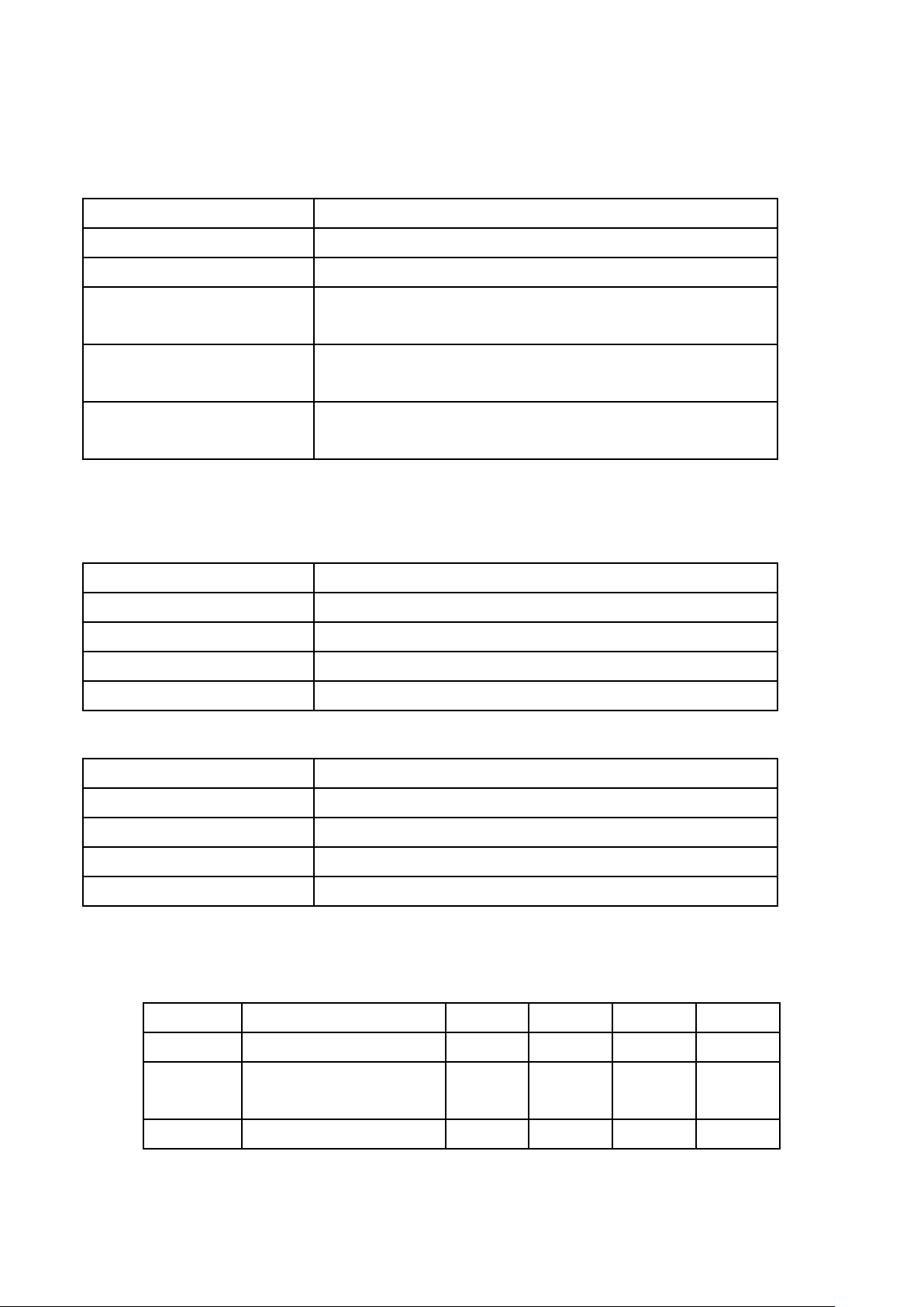
8. connect to WiFi network
9. #ifconfig => check IP.
Page 4
Bluetooth User Guide
User UART in PC/NB control AirPrime BX3210 Module
1. power supply 3.3V
2. Linux OS (USB dongle)
3. Ctrl+Alt+T => call out terminal window
4. #sudo su
5. #cd /home
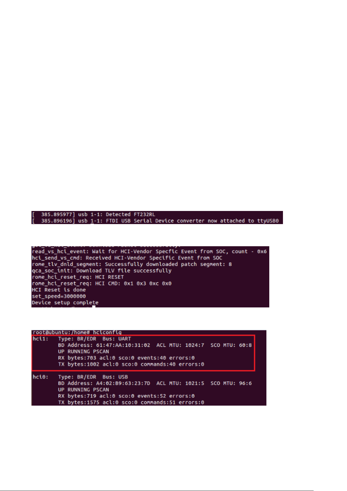
6. #Dmesg => check this device is recognized
7. # ./hciattach /dev/ttyUSB0 qca 3000000 -t120 flow
8. #hciconfig
9. #hciconfig hci0 down
Page 5

10 . #bt-adapter -a hci1 -d => search BT device
11. #bt-device -a hci1 -c B8:D5:0B:2E:07 => connect BT
12. #bt-audio -a hci1 -c B8:D5:0B:2E:B3:07
13. choice sound setting
14. choice BT device and A2DP
Page 6

15. open Rhythmbox Music player
16. play music
Page 7

Wi-Fi
2400-2483.5MHz
2.5
FCC ID: N7NBX3210
Federal Communication Commission Interference Statement
FCC Caution: Any changes or modifications not expressly approved by the party
responsible for compliance could void the user's authority to operate this equipment.
This device compl ies with Par t 15 o f the F CC Rul es. O peratio n is su bject to t he follow ing tw o
conditions: (1) This device may not cause harmful interference, and (2) this device must
accept any interference received, including interference that may cause undesired
operation.
This device and its antenna(s) must not be co-located or operating in conjunction with any
other antenna or transmitter.
For product available in the USA/Canada market, only channel 1~11 can be operated.
Selection of other channels is not possible.
IMPORTANT NOTE:
FCC Radiation Exposure Statement:
This equipment complies with FCC radiation exposure limits set forth for an uncontrolled
environment. This equipment shoul d be installed and operated with mini m um di s t anc e 20cm
between the radiator & your body.
(KDB 996369 D03 OEM Manual 2019 Feb. 01)
This module is intended for OEM integrators under the following conditions:
FCC: This module is certified pursuant to two Part 15 rules sections(15.407, 15.247).
This module has been approved to operate with the antenna types listed below, with the
maximum permissible gain indicated, and must inclu de 0.5 dB (2.4GHz) and 1.4 dB (5GHz)
cable loss compensation.
Technology Frequency Band Antenna Type Model Number Gain(dBi)
Bluetooth 2400-2483.5MHz
Wi-Fi 5150-5850MHz 5
2.5
Dipole USI05-220170
Page 8

The OEM integrator is still responsible for
1. ensuring that the end-user has no manual instructions to remove or install module
2. the FCC compliance requirement of the end product, which integrates this module.
Information on test modes and additional testing requirements
1. This module is restricted to integration into hosts for indoor use only.
2. This module has been approved under stand-alone configuration.
3. OEM integrator has be limited the operation channels in channel 1-11 for 2.4GHz band.
4. The separate approval is req ui red for al l ot her op er at ing configurations, inc luding portable
configurations with respect to Part 2.1093 and different antenna configurations.
5. The information on how to configure test modes for host product evaluation for different
operational conditions for a stand-alone modular transmitter in a host, versus with multiple,
simultaneously transmitting modules or other transmitters in a host can be found at KDB
Publication 996369 D04.
Additional testing, Part 15 Subpart B disclaimer
Appropriate measure m ents (e. g . 15 B co mpli a nc e) and if appli cable additional equip ment
authorizations (e.g. SDoC) of the host product to be addressed by the
integrator/manufacturer.
This module is only FCC authorized for the specific rule parts 15.247, 15.407 listed on the
grant, and the host product manufacturer is responsible for compliance to any other FCC
rules that apply to the host product as being Part 15 Subpart B compliant.
Label of the end product:
The host product must be labeled in a visible area with the following "Contains TX FCC ID:
N7NBX3210".
The end product shall bear the followi ng 15.19 statement: This device complies with part 15
of the FCC Rules. Operation is subject to the following two conditions: (1) This devic e may
not cause harmful interference, and (2) this device must accept any interference received,
including interference that may cause undesired operation.
The user manual of the end product should include:
Any changes or modifications not expressly approved by the party responsible for
compliance could void the user's authority to operate this equipment.
The antenna(s) use d for this t rans mitter must be instal le d to pr ovi de a separ ation dis tance o f
Page 9

at least 20 cm from all persons.
This device complies w ith par t 15 of the FC C Rul es. Oper atio n is subj ect to th e foll owi ng tw o
conditions: (1) This device may not cause harmful interference, and (2) this device must
accept any interference received, including interference that may cause undesired
operation.
This device is restricted to indoor use.
The antenna(s) used for this transmitter must not transmit simultaneously with any other
antenna or transmitter.
Page 10

Communication Business Group / Product Development Division
Product
No.
SOURCE
ORGANIZATION
:
WP/RD
/
WM/HW
Document No. Rev. 1.0
Project Code
Model No.
BX3210 EVB
Euclid BX3210 PCB Specification for
EV Board
Prepared by︰
Checked by︰
Approved by︰
Concurrence︰
Cren Yen Date : 2018-08-09
Date :
Date :
Date :
Page 11

Document
released
by
WP/RD/WM/HW
Date.
Page
Description
Euclid BX3210 EVB PCB Spec.
Revision History
Doc No.
2018-08-09
Rev
1.0
2
Version
No.
Revised
Date
1.0 2018.08.09
Revised by Description Notes
Cren Yen Preliminary Release
The content of this document is to be treated as strictly confidential and is not to be disclosed, reproduced or used
Page 12

Document
released
by
WP/RD/WM/HW
Date.
Page
Description
Doc No.
2018-08-09
Euclid BX3210 EVB PCB Spec.
Rev
1. Scope: This PCB SPEC is for EV board of BX3210 EVB. This document define the PCB
(Printed Circuit Board) manufacturing SPEC. Due to this product are applied in wireless
communication field, so all the SPEC defined in this document should be followed strictly in
order to control the line impedance and parasitic effects. Any changes or modification must
have written agreement of USI’s engineer.
2. PCB Thickness: 1400 um +/- 100um
3. PCB size: follow gerber file
4. Four Layer PCB
5. PCB Material: FR4, ,εr: 4.25 +/-0.2, Color Green, both sides.
6. Layer Stack:
- Layer 1: Component Top
- Layer 2: GND layer
- Layer 3: POWER layer
1.0
3
- Layer 4: Component Bottom
7. The PCB stack is as follows: (unit :um)
Layer Thickness Tolerance
Solder Mask
L1
P.P
250 +/- 15
L2
Core
720 +/- 50
L3
P.P
250 +/- 15
L4
Solder mask
Total Thickness: 1400 um +/- 100 um
30 +/- 15
30 +/- 10
30 +/- 10
30 +/- 10
30 +/- 10
30 +/- 15
The content of this document is to be treated as strictly confidential and is not to be disclosed, reproduced or used
Page 13

Doc No.
Document
released
by
WP/RD/WM/HW
Date.
Page
Description
Euclid BX3210 EVB PCB Spec.
8. PCB pad : 化金 0.0762um +/- 0.0457 um, Nickel min 3um.
9. Via type : L1-L4 , PTH , minimum via : 10mil hole / 20mil ring
Impedance control is required for the following picture.
RF traces @ LAYER 1 reference to Layer 2 , width: 17mil ,
Please adjust the trace width to fit 50 ohm. (in Red)
2018-08-09
Rev
1.0
4
==RF traces @ LAYER 2 reference to Layer 1, 3, width: 9mil
Please adjust the trace width to fit 50 ohm. (in Purple)
10. Panel
Attached
PCB area : Tolerance: +/- 0.2mm
The content of this document is to be treated as strictly confidential and is not to be disclosed, reproduced or used
 Loading...