

Page 1
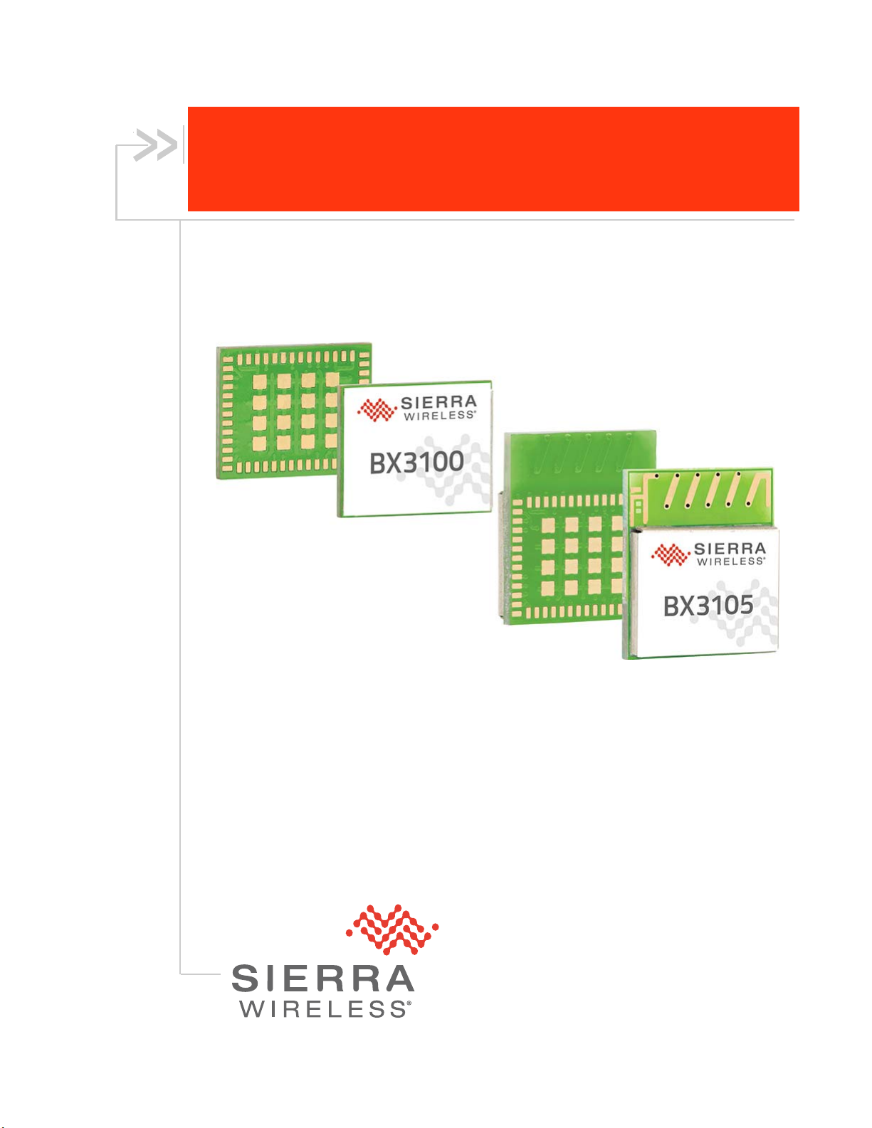
AirPrime BX3100/BX3105
Wi-Fi/BT Module
Hardware Integration Guide
41112607
Rev 3
Page 2

Hardware Integration Guide
Important
Notice
Safety and
Hazards
Due to the nature of wireless communications, transmission and reception of data can
never be guaranteed. Data may be delayed, corrupted (i.e., have errors) or be totally
lost. Although significant delays or losses of data are rare when wireless devices such
as the Sierra Wireless modem are used in a normal manner with a well-constructed
network, the Sierra Wireless modem should not be used in situations where failure to
transmit or receive data could result in damage of any kind to the user or any other
party, including but not limited to personal injury, death, or loss of property. Sierra
Wireless accepts no responsibility for damages of any kind resulting from delays or
errors in data transmitted or received using the Sierra Wireless modem, or for failure
of the Sierra Wireless modem to transmit or receive such data.
Do not operate the Sierra Wireless modem in areas where blasting is in progress,
where explosive atmospheres may be present, near medical equipment, near life
support equipment, or any equipment which may be susceptible to any form of radio
interference. In such areas, the Sierra Wireless modem MUST BE IN AIRPLANE
MODE OR POWERED OFF. The Sierra Wireless modem can transmit signals that
could interfere with this equipment.
Do not operate the Sierra Wireless modem in any aircraft, whether the aircraft is on
the ground or in flight. In aircraft, the Sierra Wireless modem MUST BE IN
AIRPLANE MODE OR POWERED OFF. When operating, the Sierra Wireless modem
can transmit signals that could interfere with various onboard systems.
Note: Some airlines may permit the use of cellular phones while the aircraft is on the ground
and the door is open. Sierra Wireless modems may be used at this time.
Limitation of
Liability
The driver or operator of any vehicle should not operate the Sierra Wireless modem
while in control of a vehicle. Doing so will detract from the driver or operator's control
and operation of that vehicle. In some states and provinces, operating such
communications devices while in control of a vehicle is an offence.
The information in this manual is subject to change without notice and does not
represent a commitment on the part of Sierra Wireless. SIERRA WIRELESS AND ITS
AFFILIATES SPECIFICALLY DISCLAIM LIABILITY FOR ANY AND ALL DIRECT,
INDIRECT, SPECIAL, GENERAL, INCIDENTAL, CONSEQUENTIAL, PUNITIVE OR
EXEMPLARY DAMAGES INCLUDING, BUT NOT LIMITED TO, LOSS OF PROFITS
OR REVENUE OR ANTICIPATED PROFITS OR REVENUE ARISING OUT OF THE
USE OR INABILITY TO USE ANY SIERRA WIRELESS PRODUCT, EVEN IF
SIERRA WIRELESS AND/OR ITS AFFILIATES HAS BEEN ADVISED OF THE
POSSIBILITY OF SUCH DAMAGES OR THEY ARE FORESEEABLE OR FOR
CLAIMS BY ANY THIRD PARTY.
Notwithstanding the foregoing, in no event shall Sierra Wireless and/or its affiliates
aggregate liability arising under or in connection with the Sierra Wireless product,
regardless of the number of events, occurrences, or claims giving rise to liability, be in
excess of the price paid by the purchaser for the Sierra Wireless product.
Rev 3 Sep.18 2 41112607
Page 3
Preface
Patents This product may contain technology developed by or for Sierra Wireless Inc. This
product is manufactured or sold by Sierra Wireless Inc. or its affiliates under one or
more patents licensed from MMP Portfolio Licensing.
Copyright ©2018 Sierra Wireless. All rights reserved.
Trademarks Sierra Wireless
registered trademarks of Sierra Wireless, Inc.
Windows
The Bluetooth
Bluetooth SIG, Inc. and any use of such marks by Sierra Wireless is under license.
Other trademarks are the property of their respective owners.
®
and Windows Vista® are registered trademarks of Microsoft Corporation.
Contact
Information
Sales information and technical
support, including warranty and returns
Corporate and product information Web: sierrawireless.com
Revision
History
Revision
number
Release date Changes
®
, AirPrime®, AirLink®, AirVantage® and the Sierra Wireless logo are
®
word mark and logos are registered trademarks owned by the
Web: sierrawireless.com/company/contact-us/
Global toll-free number: 1-877-687-7795
6:00 am to 5:00 pm PST
1 July 2018 Document created
2 July 2018 Updated Integrated PIFA gain
3 September 2018 Updated Regulatory text
Updated Wi-Fi Radio Generic Radio Characteristics table values
Updated Bluetooth Radio Generic Radio Characteristics table values
Rev 3 Sep.18 3 41112607
Page 4

Contents
1: Introduction . . . . . . . . . . . . . . . . . . . . . . . . . . . . . . . . . . . . . . . . . . . . . . . . . . . . . . . . . . .6
1.1 Module Variants . . . . . . . . . . . . . . . . . . . . . . . . . . . . . . . . . . . . . . . . . . . . . . . . . . . . .6
1.2 General RF/Software Features . . . . . . . . . . . . . . . . . . . . . . . . . . . . . . . . . . . . . . . . .6
1.2.1 Wi-Fi . . . . . . . . . . . . . . . . . . . . . . . . . . . . . . . . . . . . . . . . . . . . . . . . . . . . . . . . .6
1.2.2 Bluetooth . . . . . . . . . . . . . . . . . . . . . . . . . . . . . . . . . . . . . . . . . . . . . . . . . . . . . .6
1.2.3 Interfaces . . . . . . . . . . . . . . . . . . . . . . . . . . . . . . . . . . . . . . . . . . . . . . . . . . . . .7
1.2.4 Configuration Utility . . . . . . . . . . . . . . . . . . . . . . . . . . . . . . . . . . . . . . . . . . . . . .7
1.3 General Hardware Features . . . . . . . . . . . . . . . . . . . . . . . . . . . . . . . . . . . . . . . . . . .7
1.3.1 Physical Dimensions and Connection Interface . . . . . . . . . . . . . . . . . . . . . . . .7
2: Functional Specifications . . . . . . . . . . . . . . . . . . . . . . . . . . . . . . . . . . . . . . . . . . . . . . .9
2.1 Features . . . . . . . . . . . . . . . . . . . . . . . . . . . . . . . . . . . . . . . . . . . . . . . . . . . . . . . . . .9
3: Technical Specifications . . . . . . . . . . . . . . . . . . . . . . . . . . . . . . . . . . . . . . . . . . . . . . .11
3.1 Environmental . . . . . . . . . . . . . . . . . . . . . . . . . . . . . . . . . . . . . . . . . . . . . . . . . . . . .11
3.2 Power Supply Ratings . . . . . . . . . . . . . . . . . . . . . . . . . . . . . . . . . . . . . . . . . . . . . . .11
3.3 Power Management . . . . . . . . . . . . . . . . . . . . . . . . . . . . . . . . . . . . . . . . . . . . . . . .11
3.4 RF . . . . . . . . . . . . . . . . . . . . . . . . . . . . . . . . . . . . . . . . . . . . . . . . . . . . . . . . . . . . . .12
3.4.1 Generic Radio . . . . . . . . . . . . . . . . . . . . . . . . . . . . . . . . . . . . . . . . . . . . . . . . .12
3.4.2 Wi-Fi Radio . . . . . . . . . . . . . . . . . . . . . . . . . . . . . . . . . . . . . . . . . . . . . . . . . . .12
3.4.3 Bluetooth Radio . . . . . . . . . . . . . . . . . . . . . . . . . . . . . . . . . . . . . . . . . . . . . . . .13
3.5 Electrical Specifications . . . . . . . . . . . . . . . . . . . . . . . . . . . . . . . . . . . . . . . . . . . . . .14
3.5.1 Absolute Maximum Ratings . . . . . . . . . . . . . . . . . . . . . . . . . . . . . . . . . . . . . .14
4: Interfaces Specification . . . . . . . . . . . . . . . . . . . . . . . . . . . . . . . . . . . . . . . . . . . . . . . .15
4.1 Overview . . . . . . . . . . . . . . . . . . . . . . . . . . . . . . . . . . . . . . . . . . . . . . . . . . . . . . . . .15
4.2 UART . . . . . . . . . . . . . . . . . . . . . . . . . . . . . . . . . . . . . . . . . . . . . . . . . . . . . . . . . . . .15
4.3 ADC/Voltage Measurement . . . . . . . . . . . . . . . . . . . . . . . . . . . . . . . . . . . . . . . . . .16
4.4 I2C Interface . . . . . . . . . . . . . . . . . . . . . . . . . . . . . . . . . . . . . . . . . . . . . . . . . . . . . .17
4.4.1 Application . . . . . . . . . . . . . . . . . . . . . . . . . . . . . . . . . . . . . . . . . . . . . . . . . . . .17
4.5 I2S Interface (Digital Audio) . . . . . . . . . . . . . . . . . . . . . . . . . . . . . . . . . . . . . . . . . . .18
4.6 General Purpose Input/Output (GPIO) . . . . . . . . . . . . . . . . . . . . . . . . . . . . . . . . . .18
Rev 3 Sep.18 4 41112607
Page 5

Contents
4.7 Bootstrap Pins . . . . . . . . . . . . . . . . . . . . . . . . . . . . . . . . . . . . . . . . . . . . . . . . . . . . . 19
4.8 SPI Bus . . . . . . . . . . . . . . . . . . . . . . . . . . . . . . . . . . . . . . . . . . . . . . . . . . . . . . . . . .20
4.9 Secure Digital IO (SDIO) Interface . . . . . . . . . . . . . . . . . . . . . . . . . . . . . . . . . . . . . 21
4.10 Module Enable . . . . . . . . . . . . . . . . . . . . . . . . . . . . . . . . . . . . . . . . . . . . . . . . . . . 22
4.11 PWM . . . . . . . . . . . . . . . . . . . . . . . . . . . . . . . . . . . . . . . . . . . . . . . . . . . . . . . . . . . 22
5: General Layout Recommendations . . . . . . . . . . . . . . . . . . . . . . . . . . . . . . . . . . . . . . 23
6: Regulatory Compliance . . . . . . . . . . . . . . . . . . . . . . . . . . . . . . . . . . . . . . . . . . . . . . . . 24
6.1 United States . . . . . . . . . . . . . . . . . . . . . . . . . . . . . . . . . . . . . . . . . . . . . . . . . . . . . 24
6.2 Canada . . . . . . . . . . . . . . . . . . . . . . . . . . . . . . . . . . . . . . . . . . . . . . . . . . . . . . . . . . 25
7: Pinout . . . . . . . . . . . . . . . . . . . . . . . . . . . . . . . . . . . . . . . . . . . . . . . . . . . . . . . . . . . . . . 27
7.1 Pin Configuration . . . . . . . . . . . . . . . . . . . . . . . . . . . . . . . . . . . . . . . . . . . . . . . . . . 28
7.2 Pin Description . . . . . . . . . . . . . . . . . . . . . . . . . . . . . . . . . . . . . . . . . . . . . . . . . . . . 28
8: References . . . . . . . . . . . . . . . . . . . . . . . . . . . . . . . . . . . . . . . . . . . . . . . . . . . . . . . . . . 32
8.1 Web Site Support . . . . . . . . . . . . . . . . . . . . . . . . . . . . . . . . . . . . . . . . . . . . . . . . . . 32
8.2 Reference Documents . . . . . . . . . . . . . . . . . . . . . . . . . . . . . . . . . . . . . . . . . . . . . . 32
9: Abbreviations . . . . . . . . . . . . . . . . . . . . . . . . . . . . . . . . . . . . . . . . . . . . . . . . . . . . . . . 33
Rev 3 Sep.18 5 41112607
Page 6
1: Introduction
This document defines and illustrates the AirPrime BX310x (BX3100, BX3105) Wi-Fi/
BT Host-less module’s high-level product features, interfaces, and hardware features
(including electrical and mechanical performance criteria).
1.1 Module Variants
AirPrime BX310x module variants include:
• AirPrime BX3100— External antenna connection
• AirPrime BX3105— Embedded antenna
1.2 General RF/Software Features
1
The AirPrime BX310x is a low-power, small form-factor self-contained Wi-Fi/
Bluetooth
With an embedded software suite, the BX310x is an ideal solution for developers who
want to quickly and cost-effectively integrate Wi-Fi/ BT functionality into their products.
The following table summarizes the module’s supported wireless frequencies and
modes:
Table 1-1: Supported RF Frequencies
Technology RF band Notes
Bluetooth • v4.2 BR/EDR and BLE compliant
Wi-Fi
®
(Wi-Fi/BT) module.
2.4GHz (2.400–2.485 GHz)
• 802.11b/g/n/e/i
• Max data rate—MCS7 HT40 150 Mbps
1.2.1 Wi-Fi
The AirPrime BX310x supports 2.4 GHz Wi-Fi operation. Key features include:
• TCP/IP
• 802.11 b/g/n/e/i
• Connection methods—BSS STA, SoftAP
• Transmit power— Adjustable, up to 20 dBm (maximum)
For a list of additional supported Wi-Fi functionality, protocols, and features, see
Features on page 9.
1.2.2 Bluetooth
The AirPrime BX310x supports 2.4 GHz Bluetooth classic and BLE operation. Key
features include:
• Bluetooth v4.2 BR/EDR and BLE compliant
• SPP (Serial Port Profile)
For a list of additional supported Bluetooth functionality, protocols, and features, see
Features on page 9.
Rev 3 Sep.18 6 41112607
Page 7
Introduction
1.2.3 Interfaces
The AirPrime BX310x provides the following interfaces and peripheral connectivity:
• Power supply—See Power Supply Ratings on page 11.
• RF—See RF on page 12.
• UART serial link—See UART on page 15.
• ADC/Voltage measurement—See ADC/Voltage Measurement on page 16.
2
• I
C—See I2C Interface on page 17.
• Digital audio (I
• GPIOs—See General Purpose Input/ Output (GPIO) on page 18.
• SPI bus—See SPI Bus on page 20.
• SDIO—See Secure Digital IO (SDIO) Interface on page 21.
• Module enable— See Module Enable on page 22.
• PWM—See PWM on page 22.
2
S)—See I2S Interface (Digital Audio) on page 18.
1.2.4 Configuration Utility
The AirPrime BX310x includes a browser-based utility for device configuration. For
usage details, refer to [1] AirPrime BX310x AT Command Reference available at
source.sierrawireless.com.
1.3 General Hardware Features
1.3.1 Physical Dimensions and Connection Interface
AirPrime BX310x modules are compact, robust, fully shielded and laser-marked
modules with the dimensions noted in Table 1-2.
Table 1-2: AirPrime BX310x Dimensions
Nominal
Parameter
Length 11. 5 13.5 ±0.10 mm
Width 9.5 11.5 ±0.10 mm
Thickness 2.4 2.4 ±0.20 mm
Weight 0.56 0.65 ±0.10 g
a. Dimensions are accurate as of the release date of this document.
b. BX3100 is a CF3 xSmall module, which belongs to the Common Flexible Form Factor (CF3)
family of WWAN modules
The AirPrime BX310x module is an LGA form factor device. All electrical and
mechanical connections are made through the 70 Land Grid Array (LGA) pads on the
bottom side of the PCB. (See Figure 7-1 on page 28 for details.)
b
a
BX3105
Tol e r a n c e UnitsBX3100
Rev 3 Sep.18 7 41112607
Page 8

Hardware Integration Guide
The LGA pads have the following distribution:
Table 1-3: LGA Pad Types
Pad Type/ Quantity Dimensions Pitch
Signal Pads 54 outer pads 0.75 x0.35 mm 0.65 mm
Ground Pads 16 inner pads 1.0x1.0 mm 1.83 mm/ 1.48 mm
Rev 3 Sep.18 8 41112607
Page 9

2: Functional Specifications
2.1 Features
Table 2-1 summarizes the AirPrime BX310x module’s RF (Wi-Fi and Bluetooth),
Power, software, and hardware capabilities.
Note: Table contents are preliminary and subject to change.
Table 2-1: AirPrime BX310x Capabilities
Feature Description
• Secure boot
• Secure update
Module
Wi-Fi
• FOTA (Firmware update Over The Air)
• Sierra Wireless AirVantage support
• CF3-compliant footprint (BX3100)
• Protocols:
· 802.11 b/g/n/e/i
· 802.11 n (2.4 GHz), up to 150 Mbps; MCS0-7 in 20 / 40 MHz bandwidths
· Receiving STBC (Space-time Block Code) 2x1
· 802.11 e: QoS for wireless multimedia technology
· Additional 802.11i security features (pre-authentication, TSN, etc.)
· WMM-PS, UAPSD
· A-MPDU, A-MSDU aggregation
· Block ACK (RTS/CTS/ACK/BA)
· Fragmentation/defragmentation
· CCMP (CBC-MAC, counter model), TKIP (MIC, RC4), WAPI (SMS4), WEP
(RC4), CRC
· Frame encapsulation (802.11h/RFC 1042)
· Pre-authentication, TSN
• Supported channels— 1–14
• Data transfer (HTTP, HTTPS, MQTT, TCP/ UDP)
• Autoconnection—After device reset, automatically connects to available AP
based on previous configuration
• Infrastructure BSS Station mode/ SoftAP mode: AP mode, STA mode,
concurrent AP/STA mode
• Up to 8
• IP configuration—IP address in STA mode via DHCP or static assignment
• Authentication (security) modes: WPA, WPA2, WPA/WPA2, WPA2 Enterprise
• UMA-compliant and certified
• Open interface for various upper layer authentication schemes over EAP (e.g.
• Adaptive rate fallback algorithm
• Automatic retransmission/response on slow hosts
a
simultaneous Wi-Fi clients
TLS, PEAP, LEAP, SIM, AKA, customer-specific)
2
Rev 3 Sep.18 9 41112607
Page 10

Hardware Integration Guide
Table 2-1: AirPrime BX310x Capabilities (Continued)
Feature Description
Bluetooth
• Bluetooth v4.2 BR/EDR
• Supported channels: BT Classic
• Supported v4.2 modes: BR
(Low Energy)
b
• BT
classic mandatory features
b
and BLE compliant
b
—0–78; BLE—0–39
b
(Basic Rate); EDRb (Enhanced Data Rate); LE
• BT low-energy mandatory features
• Class 1/Class 2/Class 3 transmitter without external power amplifier
• Class 1 operation without external PA
• Enhanced power control (>30 dB dynamic control range)
• +10 dBm transmitting power
• NZIF receiver with -98 dBm sensitivity
• Modulation—p/4 DQPSK
• ACL
b
, SCOb, eSCO
b
b
, 8 DPSK
b
• Adaptive Frequency Hopping (AFH)
• BT 4.2 controller and host stack
• Service Discover Protocol (SDP)
b
b
• General Access Profile (GAP)
• Security Manage Protocol (SMP)
b
• Bluetooth Low Energy (BLE)
• ATT/GATT
• BLE Beacon
• SPP
b
b
, RFCOMM
• Profiles: Wi-Fi Autoconnection—After device reset, automatically connects to
available AP based on previous configuration.
• UART features: GATT profiles, Define personal services
• Roles—Simultaneous Central (access point) / Peripheral (client)
• Simultaneous connections:
tions
b
a
(total) simultaneous connections, including up to 3aBLE connec-
b
and BLE connections
b
/I2S
· Up to 7
· Simultaneous BT Classic
• PCM
Device configuration methods:
Configuration
• Built-in web-based configuration utility. See Configuration Utility on page 7.
• AT commands available over UART, Wi-Fi, and BT links. Refer to [1] AirPrime
BX310x AT Command Reference at source.sierrawireless.com.
• All standard IEEE802.11 security features, including WFA, WPA/WPA2, WAPI
• Secure boot
Security
• Flash encryption
• Cryptographic hardware acceleration: AES, HASH (SHA-2) library, RSA, ECC,
Random Number Generator (RNG)
Multiple power modesb to reduce power consumption: Active, Radio off, Light sleep,
Power management
a. Subject to firmware support and RAM limitations.
b. Support pending firmware upgrade.
Deep sleep, Hibernation
Sleep Patterns: Association sleep pattern, ULP sensor-monitored pattern
b
Rev 3 Sep.18 10 41112607
Page 11

3: Technical Specifications
3.1 Environmental
The environmental specifications for operation and storage of the AirPrime BX310x
are defined in Table 3-1.
Table 3-1: Environmental Specifications
Parameter Range
Ambient Operating Temperature -40°C to +85°C
3
Ambient Storage Temperature
-40°C to +105°C
(Recommended)
3.2 Power Supply Ratings
DC power is supplied via the pins described in Table 3-2 on page 11.
Note: Operation above the maximum specified operating voltage (see Table 3-8 on page 14) is
not recommended, and specified typical performance or functional operation of the device is
neither implied nor guaranteed.
Table 3-2: Power Supply Pins
Pin Name Voltage Direction Function
33 VGPIO 3.3V Output
50 VDD_3V3_RF 2.3–3.6V Input RF/Analog signal power supply
51 VDD_3V3_PA 2.3–3.6V Input Internal Power Amplifier power supply
52 VDD_PADS_BB 2.7–3.6V Input Baseband/Digital I/O power supply
Supply voltage reference for
secondary I2C interface (pins 53/54)
3.3 Power Management
The AirPrime BX310x switches between several power modes to minimize current
consumption.
Light Sleep and Deep Sleep modes are enabled via AT commands from the host.
Refer to [1] AirPrime BX310x AT Command Reference for details.
Rev 3 Sep.18 11 41112607
Page 12

Hardware Integration Guide
Table 3-3 describes the AirPrime BX310x’s supported power modes.
Table 3-3: Power Modes — Descriptions
Wi-Fi/BT
radio /
Power Mode CPU
Active On On On On Fully functional
Radio off
Light sleep
Deep sleep
a
a
a
On Off On On
Pause Off On On Wake up events will wake the module.
Off Off On On/ Off Connection data stored in RTC memory
baseband
RTC
ULP co-
processor Notes
Hibernate
a. Available in future firmware release.
a
Off Off Off Off
3.4 RF
3.4.1 Generic Radio
Measurements conducted at 25C ambient temperature.
Table 3-4: Generic Radio Characteristics
Description Min Typ Max Unit
BX3100 RF Port Impedance 50
Frequency Band 2.4 2.45 2.485 GHz
BX3105 Antenna Gain 0 dBi
3.4.2 Wi-Fi Radio
Measurements conducted at 25C ambient temperature.
Only RTC timer or specific RTC GPIOs
can wake the module.
Table 3-5: Generic Radio Characteristics
Description Min Typ Max Unit
Transmit 802.11b, CCK 1 Mbps, Conducted Tx Power, EVM and Mask Compliant 14 15.5 17 dBm
Transmit 802.11g, OFDM 6 Mbps, Conducted Tx Power, EVM and Mask Compliant 14a15.5a17adBm
Transmit 802.11n, MCS0 HT20 6.5 Mbps, Conducted Tx Power, EVM and Mask Compliant 14b15.5b17bdBm
Transmit 802.11n, MCS0 HT40 13.5 Mbps, Conducted Tx Power, EVM and Mask Compliant 14c15.5c17cdBm
Conducted Receiver Sensitivity 11b DSSS, 1 Mbps -98 -95 -93 dBm
Conducted Receiver Sensitivity 11b CCK, 11 Mbps -90 -87 -84 dBm
Conducted Receiver Sensitivity 11g OFDM, 6 Mbps -94 -91 -88 dBm
Rev 3 Sep.18 12 41112607
Page 13

Technical Specifications
Table 3-5: Generic Radio Characteristics (Continued)
Description Min Typ Max Unit
Conducted Receiver Sensitivity 11g OFDM, 54 Mbps -73 -71.5 -70 dBm
Conducted Receiver Sensitivity 11n HT20 OFDM, 72.2 Mbps -73 -71 -69 dBm
Conducted Receiver Sensitivity 11n HT40 OFDM, 135 Mbps -73 -71 -69 dBm
Conducted Harmonics 2F0 - -42 -39 dBm
Conducted Harmonics 3F0 - -54 -51 dBm
a. Channel 1&11 power is automatically reduced for FCC 15.205 band edge compliance, reduction is 2 dB.
b. Channel 1&11 power is automatically reduced for FCC 15.205 band edge compliance, reduction is 2.5 dB.
c. Channel 1 & 11 typical power is automatically reduced for FCC 15.205 band edge compliance, reduction is 3 dB.
3.4.3 Bluetooth Radio
Measurements conducted at 25C ambient temperature.
Table 3-6: Generic Radio Characteristics
Description Min Typ Max Unit
Transmit Power BR 1 Mbps 7.5 9 10.5
a
dBm
Transmit Power EDR 2 Mbps 7.5 9 10.5 dBm
Transmit Power EDR 3 Mbps 7.5 9 10.5 dBm
Transmit Power LE 1 Mbps 2.5 4 5.5 dBm
Receiver Sensitivity BR 1 Mbps -89 -88 -87 dBm
Receiver Sensitivity EDR 2 Mbps -87 -86 -85 dBm
Receiver Sensitivity EDR 3 Mbps -81 -82.5 -84 dBm
Receiver Sensitivity LE 1 Mbps -92.5 -91 -89 dBm
Out-of-band blocking performance 30 MHz~2000 MHz - -10 - dBm
Out-of-band blocking performance 2000 MHz~2400 MHz - -27 - dBm
Out-of-band blocking performance 2500 MHz~3000 MHz - -27 - dBm
Out-of-band blocking performance 3000 MHz~12.5 GHz - -10 - dBm
a. Maximum Output power is restricted by compliance to FCC 15.205 band edge to 5.5 dBm Max.
Rev 3 Sep.18 13 41112607
Page 14

Hardware Integration Guide
3.5 Electrical Specifications
3.5.1 Absolute Maximum Ratings
Table 3-7: Absolute Maximum Ratings
Parameter Min Max Units
V
Input low voltage -0.3 0.25 V
IL
V
Input high voltage 0.75 V
IH
I
Input leakage current - 50 nA
IL
V
Output low voltage - 0.1 V
OL
V
Output high voltage 0.8 V
OH
C
Input pin capacitance - 2 pF
pad
V
VDD_PADS_BB 2.7 3.6 V
IO
I
GPIO maximum drive capability - 12 mA
MAX
T
Storage temperature range -40 150 C
STR
IO
IO
3.6 V
- V
IO
IO
V
V
Table 3-8: Recommended Operating Conditions
Parameter Min Typ Max Units
V
Supply voltage (VDD_3V3_PA, VDD_3V3_RF) 2.3 3.3 3.6 V
DD
V
I/O supply voltage (VDD_PADS_BB) 2.7 3.3 3.6 V
IO
T
Operating temperature range -40 - 85 C
OPR
V
CMOS low level input voltage 0 - 0.3 V
IL
V
CMOS high level input voltage 0.7 V
IH
V
CMOS threshold voltage - 0.5 V
TH
V
IO
IO
- V
IO
IO
- V
V
Rev 3 Sep.18 14 41112607
Page 15

4: Interfaces Specification
4.1 Overview
This section describes the interfaces supported by the AirPrime BX310x embedded
module and provides specific voltage, timing, and circuit recommendations for each
interface.
4.2 UART
The AirPrime BX310x provides one UART interface for asynchronous communication
between the AirPrime BX310x module and a host device (e.g. a PC or host
processor):
• UART0— 4-wire, RS-232-compliant interface
Note: Up to two additional UART interfaces can be added by configuring GPIOs using AT
commands.
Flow control is managed using:
• RTS/CTS signals (This method is required for higher UART interface speeds.)
or
• Software XON/ XOFF
4
Table 4-1 on page 15 describes the signals used for UART0.
Table 4-1: UART0 Pins
Pin Interface Name Direction Function Voltage Level
2
3 UART0_CTS O Clear To Send, flow control
UART0
4 UART0_TXD I Transmit Data
5 UART0_RXD O Receive Data
a. If UART0 pins are not used, leave open.
Note: UART signals are named with respect to the HOST, and directions are listed with respect
to the module. For example, UART0_RXD is an output from the module to the host.
The UART interface is configurable via AT commands:
• Default configuration— 115200 (baudrate), 8 bit, no parity, no handshaking
• Baudrate considerations:
· Maximum supported—5 Mbaud
· Maximum tested— 3 Mbaud. This is the maximum baudrate supported by the
BX310x Dev Kit FTDI converter IC.
· HW handshaking is recommended above rates of 1 Mbaud and can be
enabled via AT command (AT&K3).
a
UART0_RTS I Ready To Send, flow control
VDD_PADS_BB
Rev 3 Sep.18 15 41112607
Page 16

Hardware Integration Guide
4.3 ADC/Voltage Measurement
The AirPrime BX310x provides a general purpose ADC (Analog to Digital Converter)
input, which can sample multiple inputs configured using AT commands.
Pins VDET_1, VDET_2, SENSOR_VP, and SENSOR_VN are used to measure
single-ended analog voltages referenced to ground. The voltage on these pins is read
via an AT command.
Noise can have a large impact on sensitive voltage measurements. To improve the
accuracy of small voltage level measurements, a100 nF capacitor to ground is
recommended on the input to the VDET_1, VDET_2, SENSOR_VP, and
SENSOR_VN pins.
· Common baud rates are supported—any baud rate in the supported range
can be selected via AT+IPR=<uart_baud_rate> command. The device
automatically configures the clock dividers appropriately for the chosen baud
rate.
· Baud rates are persistent post-reset.
· Recommendation— Add series termination resistors close to the module in
the UART lines for management of clock harmonics. 499 resistors are
recommended.
Table 4-2: ADC Interface Pins
Pin Signal name
18 VDET_1 I
19 VDET_2 I
a. Leave open any pins that are not used.
b. Signal direction with respect to the module.
Direction
Table 4-3: Voltage-measurement GPIO Pins
Pin Signal Name
31 SENSOR_VP I
32 SENSOR_CAPP I
34 SENSOR_CAPN I
36 SENSOR_VN I
a. Leave open any pins that are not used.
b. Signal direction with respect to the module.
a
b
Analog to Digital Converter VDD_PADS_BB
Direction
Function Voltage Level
a
b
Voltage level
VDD_PADS_BB
Access to a Hall effect sensor is supported via firmware, and is selected using AT
commands.
The sensor pins (SENSOR_VP or SENSOR_VN) will trigger an input perturbation
(glitch) lasting for 80 ns when the ADC or Hall sensor is initialized.
Rev 3 Sep.18 16 41112607
Page 17

Interfaces Specification
AirPrime BX310x
Wi-Fi/BT Module
Customer
Application
I2C1_SDA
I2C1_SCL
2.2K
2.2K
VDD_PADS_BB
I2C2_SCL
I2C2_SDA
2.2K
VGPIO
2.2K
4.4 I2C Interface
The AirPrime BX310x module provides two I2C (Inter-Integrated Circuit) dedicated
serial ports (bus interface) based on [2] The I2C Bus Specification, Version 2.1,
January 2000 (Phillips Semiconductor document number 9398 393 40011).
The interfaces use the pins indicated in Table 4-4.
Table 4-4: I2C Interface Pins
a
Pin Signal name Direction Function Voltage Level
9 I2C1_SCL I/O Primary I2C interface
VDD_PADS_BB
17 I2C1_SDA I/O Primary I2C interface
53 I2C2_SDA I/O Secondary I2C interface
VGPIO
54 I2C2_SCL I/O Secondary I2C interface
a. Leave open any pins that are not used.
This implementation of the I
2
C interface includes the following characteristics:
• Supported voltage:
· Primary I2C (3.3 V, configurable)
· Secondary I2C (3.3 V)
• Standard-mode interface— Data transfer rates up to 100 kbit/s
• Fast-mode interface— Data transfer rates up to 400 kbit/s)
• Master mode operation
• Addressing modes — 7-bit; 10-bit; Dual addressing mode
External 2.2 k pull-up resistors must be applied to I
2
C signals (see Figure 4-1 on
page 17).
2
For I
C bus details, including I2C bus waveform and timing details, refer to the
I2C Bus Specification.
Rev 3 Sep.18 17 41112607
4.4.1 Application
Figure 4-1: Example of I2C Bus Application
Page 18

Hardware Integration Guide
4.5 I2S Interface (Digital Audio)
Note: Interface support is forthcoming.
The AirPrime BX310x provides a 4-wire I2S (digital audio) interface that can be used
to transfer serial digital audio to or from an external stereo DAC/ADC, and supports
the following features:
• Modes—Master, Slave
• Transmission format— Full duplex, Half duplex
• Resolution (bits per frame) — 8, 16, 32, 40, 48
• Channels—Input, Output
• Bit clock—10 kHz–40 MHz
• Supported audio interfaces (forthcoming)—PDM (Pulse Density Modulation),
The interface uses the pins indicated in Table 4-5.
BT PCM (Pulse Code Modulation)
Table 4-5: I2S Interface Pins
Pin Signal name
16 I2S_MCLK O I2S MasterClock
24 I2S_DO O I2S Data Out
25 I2S_DI I I2S Data In
26 I2S_LRCLK I/O I2S Left-Right Clock (Word Select)
27 I2S_BCLK I/O I2S Bit Clock
a. Leave open any pins that are not used.
b. Signal direction with respect to the module.
Direction
a
b
Function Voltage Level
VDD_PADS_BB
4.6 General Purpose Input/Output (GPIO)
The AirPrime BX310x defines several GPIOs for customer use, as described in
Table 4-6 and Table 4-7.
Note: The pins carrying the ‘Alternate function’ GPIOs are multi-function. The alternate interfaces (SDIO or SPI) can be selected via an AT command.
Table 4-6: GPIO Pins (Dedicated)
Pin Signal Name Direction Default State Function Voltage Level
14 GPIO(5) I/O Pull high
35 GPIO(27) I/O No pull
a. Leave open any pins that are not used.
b. Pulled high internally
c. Internal configuration — no internal pull-ups
a
b
General purpose I/O VDD_PADS_BB
c
Rev 3 Sep.18 18 41112607
Page 19

Interfaces Specification
Table 4-7: GPIO Pins (Alternate function)
a
Pin Signal Name Direction Default State Function Voltage Level
9 GPIO(23)
16 GPIO(0) Pull high
17 GPIO(25) No pull
18 GPIO(34) No pull
19 GPIO(35) No pull
24 GPIO(32) No pull
25 GPIO(33) No pull
26 GPIO(18) No pull
27 GPIO(26) No pull
31 GPIO(36) No pull
32 GPIO(37) No pull
I/O
34 GPIO(38) No pull
36 GPIO(39) No pull
42 GPIO(15) Pull highc
43 GPIO(12) Pull low
44 GPIO(14) Pull high
45 GPIO(13) Pull high
46 GPIO(2) Pull low
47 GPIO(4) Pull low
53 GPIO(16) No pull
54 GPIO(17) No pull
No pull
b
c
b
b
b
b
b
b
b
b
b
General purpose I/O VDD_PADS_BB
b
b
d
e
c
c
e
e
b
b
a. Leave open any pins that are not used.
b. Internal configuration—no internal pull-ups
c. Pulled high internally
d. GPIO(15) default state (pull HIGH) enables UART boot messaging. To disable UART boot mes-
sages, drive GPIO(15) LOW prior to boot.
e. Pulled low internally
4.7 Bootstrap Pins
The GPIOs listed in Table 4-8 are used as Bootstrap pins during start-up.
Rev 3 Sep.18 19 41112607
Page 20

Hardware Integration Guide
Table 4-8: GPIO Bootstrap Functions
GPIO Function Default State Default Function Alternative
0 Boot Source High, Internal pull 45 k
2 Boot Source High, Internal pull 45 k
5
SDIO Slave Timing
15 (MTDO) High, Internal pull 45 k
12 (MTDI) SDIO Interface Voltage Low, Internal pull 45 k 3.3V 1.8V (Not supported)
High, Internal pull 45 k
Boot from Internal Flash Download to Flash (Disabled)
Rising Edge Input & Output See Table 4-9.
Table 4-9: SDIO Slave Timing Configuration
GPIO(5) GPIO(15) Configuration
Low Low Falling Edge Input & Output
Low High Rising Edge Input, Falling Edge Output
High Low Falling Edge Input, Rising Edge Output
High High Rising Edge Input & Output
4.8 SPI Bus
Note: Interface support is forthcoming.
The AirPrime BX310x provides one 6-wire Serial Flash SPI-compatible interface
(SPI Master).
Note: Traditional 5-wire (MOSI/MISO/SCLK/CS/SRDY) SPI Slave interface can also be
implemented over this same interface.
Table 4-10 describes the SPI interface pins for both configurations (5- and 6-wire).
Note: The pins carrying the SPI interface ar e multi-function. The alternate interfaces (SDIO or
GPIO) can be selected via an AT command.
Table 4-10: SPI Pin Descriptions
SPI Master SPI Slave
Pin
42 HSPICS0 CS O I SPI Chip Select
43 HSPIQ MISO I O MISO
44 HSPICLK SCLK O I SPI Clock
a
Direction
b
Function6-Wire Signal Name 5-Wire Signal Name Master Slave
Rev 3 Sep.18 20 41112607
Page 21

Table 4-10: SPI Pin Descriptionsa (Continued)
Interfaces Specification
SPI Master SPI Slave
Pin
45 HSPID MOSI O I MOSI
46 HSPIWP - O - Write Protect (M)
47 HSPIHD SRDY O O Hold
a. Leave open any pins that are not used.
b. Signal direction with respect to the module.
Direction
b
Function6-Wire Signal Name 5-Wire Signal Name Master Slave
4.9 Secure Digital IO (SDIO) Interface
Note: Interface support is forthcoming.
The AirPrime BX310x defines one SDIO slave-controller interface (SD 2.0-compliant),
which supports connections to SD memory and I/O cards.
The following features are supported:
• SPI/1-bit/4-bit modes
• Data transfer rates — 0–50 MHz
• Block size—Up to 512 bytes
• Interrupts— Module-initiated and host-initiated
• Module-initiated data transfer via host interrupt
• Configurable features— Sampling, driving clock edge
• Registers for direct access by host
Table 4-11 describes the signals used for SDIO.
Note: The pins carrying the SDIO interface are multi-function. The alternate interfaces (GPIO
or SPI) can be selected via an AT command.
Table 4-11: SDIO Pin Descriptions
Pin Signal Name
42 SD_CMD I/O SDIO command
43 SD_DATA2 I/O SDIO data bit 2
44 SD_CLK O SDIO clock
45 SD_DATA3 I/O SDIO data bit 3
46 SD_DATA0 I/O SDIO data bit 0
47 SD_DATA1 I/O SDIO data bit 1
a. Leave open any pins that are not used.
Direction
a
Function
Rev 3 Sep.18 21 41112607
Page 22

Hardware Integration Guide
SDIO is particularly susceptible to tracking impedance and length variations between
the SDIO tracks. Ensure that controlled impedance tracking is used, and minimize
tracking length between the module and SD slave device. Add series resistor
footprints at the host end to decrease the drive current and reduce potential
interference, and match the length of all the SD tracks to within 1 mm.
SDIO tracking can cause significant radiated interference at integer multiples of the
SD clock frequency, which can be picked up by the BX310x antenna. Bury SDIO
tracks between ground planes and ensure stitching ground vias are placed throughout
the board surrounding the SDIO tracking.
SDIO timing during the boot process is provided by GPIO(5) and GPIO(15). See
Table 4-9 on page 20 for details.
4.10 Module Enable
The AirPrime BX310x uses the ENABLE (Module Enable) signal to turn the module
on/off:
• Turn module on— Drive ENABLE high (to VDD_PADS_BB)
• Turn module off—Drive ENABLE low (to 0V)
Table 4-12: Enable Pin Description
Pin Signal Name
b
37
To avoid a possible implementation-dependent issue where enabling/disabling Wi-Fi
functionality could cause a perturbation (glitch) on the power supply rails that impacts
module operations, a short delay (1 ms recommended) is required for the power
supply to stabilize before enabling the module.
If ENABLE is controlled by the Host, the host implements the delay (from the time the
supply is present) before driving ENABLE high.
If ENABLE is hard-wired to the supply (VDD_PADS_BB), an RC circuit (10k &
0.1uF) is required. The RC circuit will create the required delay, allowing the supply to
stabilize before ENABLE is pulled high.
Do not leave this pin unconnected.
ENABLE I Start/stop module VDD_PADS_BB
a. Signal direction with respect to the module.
b. Do not leave this pin unconnected.
Direction
a
Function Voltage Level
4.11 PWM
The AirPrime BX310x supports the use of PWM functionality on GPIOs (GPIO(5) and
GPIO(27)) via AT command configuration. Refer to [1] AirPrime BX310x AT Command
Reference for details.
Rev 3 Sep.18 22 41112607
Page 23

5: General Layout Recommendations
In addition to specific requirements for the antenna implementation and clearance of
the BX3105 detailed in this document, good mixed-signal layout practices should be
followed:
• Avoid tracking of high frequency signals near the RF sections of the module.
• Ensure plenty of ground vias throughout the application board.
• Tightly tie ground planes together throughout the application board.
• BX3100 RF tracking to application board antenna or RF connector:
· Use 50 impedance controlled tracks.
· Do not track near sources of digital interference.
· Provide continuous unbroken ground plane reference.
· Avoid multiple layer changes.
• Supply decoupling should be placed as close to the supply pins as possible.
• Avoid long digital tracks on surface layers— they may support significant RF
harmonic content.
5
Rev 3 Sep.18 23 41112607
Page 24

6: Regulatory Compliance
FCC ID: N7NBX31A
Caution: Unauthorized modifications or changes not expressly approved by Sierra Wireless
could void compliance with regulatory rules, and thereby your authority to use this equipment.
The BX3100/BX3105 module is designed to meet the requirements of the following
regulatory bodies and regulations, where applicable:
• Federal Communications Commission (FCC) of the United States
• Innovation, Science and Economic Development Canada (ISED)
• Ministry of Internal Affairs and Communications (MIC) of Japan
• Radio Equipment Directive of the European Union
• Ministry of Industry and Information Technology (People’s Republic of China)
• The National Communications Commission (NCC) of Taiwan, Republic of China
• The National Telecommunications Agency (ANATEL)
• National Radio Research Agency (South Korea)
Note: To determine whether specific approvals have been received or to obtain the anticipated
schedule for approvals, please contact your Sierra Wireless account representative.
Upon commercial release, the following industry certification will have been obtained,
where applicable:
• Bluetooth SIG
6
Additional certifications and details on specific country approvals may be obtained
upon customer request — contact your Sierra Wireless account representative for
details.
Additional testing and certification may be required for the end product with an
embedded BX3100/BX3105 module and are the responsibility of the OEM. Sierra
Wireless offers professional services-based assistance to OEMs with the testing and
certification process, if required.
6.1 United States
The BX3100/BX3105 module has been certified by the Federal Communications
Commission under FCC ID: N7NBX31A. The BX3105 module is certified with an
on-board antenna, while the BX3100 module is certified with an external antenna.
Integrators may use the BX3100/ BX3105 modules in their end products without
additional FCC certification if they meet the following conditions. Otherwise, additional
FCC approval must be obtained.
1. Only antennas of the same type and with equal or less gains as shown in
Table 6-1 may be used. Other types of antennas and/or higher gain antennas
may require additional authorization for operation.
2. The end product integrating the BX3100 module must use the RF trace design
approved with the BX3100 module. Details of the trace design can be obtained
from Sierra Wireless upon request.
3. At least 6 cm separation distance between the antenna and the user’s body, or
2.5 cm separation distance when the end product is designed or intended for use
Rev 3 Sep.18 24 41112607
Page 25

Regulatory Compliance
IC: 2417C-BX31A
on extremities, or mainly operated in extremity-only exposure conditions, i.e.,
hands, wrists, feet and ankles, must be maintained at all times.
4. The regulatory label on the end product must include the text “Contains FCC ID:
N7NBX31A” and the following compliance statement:
This device complies with Part 15 of the FCC Rules. Operation is subject to the
following two conditions: (1) This device may not cause harmful interference, and
(2) this device must accept any interference received, including interference that
may cause undesired operation.
5. A user manual with the end product must clearly indicate the operating requirements and conditions that must be observed to ensure compliance with current
FCC RF exposure guidelines.
6. End users must not be provided with access to configuration options to change
technical parameters of the BX3100/BX3105 module, except as permitted by the
FCC rules.
The end product with an embedded BX3100/BX3105 module may also need to meet
the requirements in FCC Part 15 Subpart B for unintentional radiators and be properly
authorized.
Table 6-1: Antenna Specifications
Module Antenna Type Maximum Gain
BX3105 Integrated PIFA -1.65 dBi
BX3100
Monopole 0dBi
Dipole 2.5 dBi @ 2.4 GHz
6.2 Canada
This radio transmitter IC: 2417C-BX31A has been approved by Innovation, Science
and Economic Development Canada to operate with the antenna types listed below,
with the maximum permissable gain indicated. Antenna types not included in this list
that have a gain greater than the maximum gain indicated for any type listed are
strictly prohibited for use with this device.
Integrators may use the BX3100/ BX3105 modules in their end products without
additional ISED certification if they meet the following conditions. Otherwise,
additional ISED approval must be obtained.
1. Only antennas of the same type and with equal or less gains as shown in
Table 6-1 may be used. Other types of antennas and/or higher gain antennas
may require additional authorization for operation.
2. The end product integrating the BX3100 module must use the RF trace design
approved with the BX3100 module. Details of the trace design can be obtained
from Sierra Wireless upon request.
3. At least 4.5 cm separation distance between the antenna and the user’s body, or
3 cm separation distance when the end product is designed or intended for use
on extremities, or mainly operated in extremity-only exposure conditions, i.e.,
hands, wrists, feet and ankles, must be maintained at all times.
Rev 3 Sep.18 25 41112607
Page 26

Hardware Integration Guide
4. The regulatory label on the end product must include the text “Contains
5. A user manual with the end product must clearly indicate the operating require-
6. End users must not be provided with access to configuration options to change
IC: 2417C-BX31A” and the following compliance statement:
This device complies with Industry Canada license-exempt RSS standard(s).
Operation is subject to the following two conditions: (1) This device may not cause
interference, and (2) this device must accept any interference, including interference that may cause undesired operation of the device.
Le présent appareil est conforme aux CNR d'Industrie Canada applicables aux
appareils radio exempts de licence. L'exploitation est autorisée aux deux conditions suivantes: (1) l'appareil ne doit pas produire de brouillage, et (2) l'utilisateur
de l'appareil doit accepter tout brouillage radioélectrique subi, même si le brouillage est susceptible d'en compromettre le fonctionnement.
ments and conditions that must be observed to ensure compliance with current
ISED RF exposure guidelines.
technical parameters of the BX3100/BX3105 module, except as permitted by the
ISED rules.
Rev 3 Sep.18 26 41112607
Page 27

7: Pinout
The system interface of the AirPrime BX310x is through the LGA pattern on the
bottom of the PCB.
AirPrime BX310x pins are divided into three functional categories:
• Core functions and associated pins— Cover all the mandatory features for M2M
connectivity and will be available by default across all CF3 family of modules.
These Core functions are always available and always at the same physical pin
locations. A customer platform using only these functions and associated pins is
guaranteed to be forward and/or backward compatible with the next generation of
CF3 modules.
• Extension functions and associated pins—Bring additional capabilities to the
customer. Whenever an Extension function is available on a module, it is always
at the same pin location.
• Custom functions and associated pins— These are module-specific and make
use of specific chipset functions and I/Os.
Warning: Custom features should be used with cautio n as ther e is no guarantee that the
custom functions available on a given module will be available on other CF3 modules.
Pins marked as "Leave open" or "Reserved" should not be used or connected.
7
Rev 3 Sep.18 27 41112607
Page 28

Hardware Integration Guide
7.1 Pin Configuration
Figure 7-1 illustrates the pin configuration of the AirPrime BX310x module.
Figure 7-1: Pin Configuration (Bottom View)
7.2 Pin Description
Table 7-1 on page 28 lists detailed information for the LGA pins.
Important: Leave open all pins that are not used.
Table 7-1: Pin Definitions
Pin Signal name Group I/O
1 Reserved NoConnect - - - - E
2 UART0_RTS_GPIO(22) UART0 I VDD_PADS_BB PU L UART0 Request To Send C
3 UART0_CTS_GPIO(19) UART0 O VDD_PADS_BB PU L UART0 Clear To Send C
4 UART0_TXD UART0 I VDD_PADS_BB PU L UART0 Transmit Data C
5 UART0_RXD UART0 O VDD_PADS_BB PU L UART0 Receive Data C
6 Reserved NoConnect - - - - - E
a
Vol t age
PU/
PD
b
Active
c
Function Type
d
Rev 3 Sep.18 28 41112607
Page 29

Table 7-1: Pin Definitions (Continued)
Pinout
PU/
Pin Signal name Group I/O
a
Vol t age
PD
b
Active
c
Function Type
7 Reserved NoConnect - - - - - E
8 Reserved NoConnect - - - - - E
GPIO(23) GPIO I/O
9
VDD_PADS_BB
NP SW General Purpose I/O C
I2C1_SCL I2C1 I/O PUE L Primary I2C interface—Clock
10 Reserved NoConnect - - - - - C
11 Reserved NoConnect - - - - - C
12 Reserved NoConnect - - - - - C
13 Reserved NoConnect - - - - - C
14 GPIO(5) GPIO I/O VDD_PADS_BB NP SW General Purpose I/O E
15 Reserved NoConnect - - - - - E
I2S_MCLK I2S O
16
VDD_PADS_BB
NP H I2S Master Clock E
GPIO(0) GPIO I/O NP SW General Purpose I/O
GPIO(25) GPIO I/O
17
VDD_PADS_BB
NP SW General Purpose I/O E
I2C1_SDA I2C1 I/O PUE L Primary I2C interface —Data
VDET_1 VoltMeasure I
18
VDD_PADS_BB
NP H ADC input for voltage measurement C
GPIO(34) GPIO I/O NP SW General Purpose I/O
d
VDET_2 VoltMeasure I
19
VDD_PADS_BB
NP H ADC input for voltage measurement C
GPIO(35) GPIO I/O NP SW General Purpose I/O
20 Reserved NoConnect - - - - - C
21 Reserved NoConnect - - - - - C
22 Reserved NoConnect - - - - - C
23 Reserved NoConnect - - - - - C
I2S_DO I2S O
24
VDD_PADS_BB
PD H I2S Data Out C
GPIO(32) GPIO I/O NP SW General Purpose I/O
I2S_DI I2S I
25
VDD_PADS_BB
PD H I2S Data In C
GPIO(33) GPIO I/O NP SW General Purpose I/O
I2S_LRCLK I2S I/O
26
VDD_PADS_BB
PD L/H I2S Left-Right Clock (Word Select) C
GPIO(18) GPIO I/O NP SW General Purpose I/O
I2S_BCLK I2S I/O
27
VDD_PADS_BB
PD H I2S Bit Clock C
GPIO(26) GPIO I/O NP SW General Purpose I/O
28 GND Ground 0V 0V - - Ground C
29 Reserved NoConnect - - - - - E
Rev 3 Sep.18 29 41112607
Page 30

Hardware Integration Guide
Table 7-1: Pin Definitions (Continued)
PU/
Pin Signal name Group I/O
a
Vol t age
PD
b
Active
c
Function Type
30 GND Ground 0V 0V - - Ground C
GPIO(36) GPIO I/O
31
VDD_PADS_BB
NP SW General Purpose I/O C
SENSOR_VP VoltMeasure I NP H ADC input for voltage measurement
GPIO(37) GPIO I/O
32
VDD_PADS_BB
NP SW General Purpose I/O C
SENSOR_CAPP VoldMeasure I NP H ADC input for voltage measurement
33 VGPIO Power O 3.3V Reference voltage output C
GPIO(38) GPIO I/O
34
VDD_PADS_BB
NP SW General Purpose I/O C
SENSOR_CAPN VoltMeasure I NP H ADC input for voltage measurement
35 GPIO(27) GPIO I/O VDD_PADS_BB NP L General Purpose I/O E
GPIO(39) GPIO I/O
36
VDD_PADS_BB
NP SW General Purpose I/O C
SENSOR_VN VoltMeasure I NP H ADC input for voltage measurement
37 ENABLE Control I VDD_PADS_BB L Turn module on/off C
38 Reserved NoConnect - - - - - E
39 GND Ground 0V 0V - - Ground C
40 RF_MAIN RF I/O - -
(BX3100) RF antenna, DC blocked
(BX3105) Leave pin unconnected
d
C
41 GND Ground 0V 0V - - Ground C
SD_CMD SDIO I/O
42
HSPICS0 SPI I/O NP SW SPI Chip Select C
VDD_PADS_BB
NP H SDIO Command E
GPIO(15) GPIO I/O NP SW General Purpose I/O E
SD_DATA2 SDIO I/O
43
HSPIQ SPI I/O NP SW SPI Data In C
VDD_PADS_BB
NP H SDIO Data bit 2 E
GPIO(12) GPIO I/O NP SW General Purpose I/O E
SD_CLK SDIO I/O
44
HSPICLK SPI I/O NP SW SPI Clock (output from Master) C
VDD_PADS_BB
NP H SDIO Clock E
GPIO(14) GPIO I/O NP SW General Purpose I/O E
SD_DATA3 SDIO I/O
45
HSPID SPI I/O NP SW SPI Data Out C
VDD_PADS_BB
NP H SDIO Data bit 3 E
GPIO(13) GPIO I/O NP SW General Purpose I/O E
SD_DATA0 SDIO I/O
46
HSPIWP SPI O NP SW SPI Write Protect E
VDD_PADS_BB
NP H SDIO Data bit 0 E
GPIO(2) GPIO I/O NP SW General Purpose I/O E
Rev 3 Sep.18 30 41112607
Page 31

Table 7-1: Pin Definitions (Continued)
Pinout
Pin Signal name Group I/O
a
Vol t age
SD_DATA1 SDIO I/O
47
HSPIHD SPI O NP SW SPI Hold E
VDD_PADS_BB
PD
b
Active
c
Function Type
NP H SDIO Data bit 1 E
GPIO(4) GPIO I/O NP SW General Purpose I/O E
48 Reserved NoConnect - - - - - E
49 Reserved NoConnect - - - - - E
2.8 (Min)
PU/
50 VDD_3V3_RF Power I
3.3V (Typ)
- - 3.3v nominal supply for Analog/ RF C
3.6 (Max)
51 VDD_3V3_PA Power I
52 VDD_PADS_BB Power I
GPIO(16) GPIO I/O
53
2.8 (Min)
3.3V (Typ)
3.6 (Max)
2.7 (Min)
3.3V (Typ)
3.6 (Max)
VGPIO
- -
- -
NP SW General Purpose I/O C
3.3v nominal supply for Internal
Power Amplifier
3.3v nominal supply for Baseband
and Digital I/O
I2C2_SDA I2C2 I/O PUE L Primary I2C interface — Data
GPIO(17) GPIO I/O
54
VDD_PADS_BB
NP SW General Purpose I/O C
I2C2_SCL I2C2 I/O PUE L Primary I2C interface—Clock
d
C
C
G1–
Ground Ground 0V 0V - - Ground C
G16
a. I/O: Signal direction with respect to the module
b. PU/ PD: NP— No Pull; PD — Pull Down; PU — Pull Up; PUE — Pull Up External
c. Active: H — High; L—Low; SW— Software defined
d. Type: C— Core; E — Extended; K — Custom
Rev 3 Sep.18 31 41112607
Page 32

8: References
8.1 Web Site Support
Check http://source.sierrawireless.com for the latest documentation available for the
AirPrime BX310x.
8.2 Reference Documents
[1] AirPrime BX310x AT Command Reference
Reference number: 41111445
[2] The I
2
C Bus Specification, Version 2.1, January 2000 (Phillips Semiconductor
document number 9398 393 40011)
8
Rev 3 Sep.18 32 41112607
Page 33

9: Abbreviations
Table 9-1: Acronyms and Definitions
Acronym or term Definition
AFH Adaptive Frequency Rate Hopping
AP Access Point
BLE Bluetooth Low Energy
BR Basic Rate
BSS Basic Service Set
BT Bluetooth (Classic)
EDR Enhanced Data Rate
EDR Enhanced Data Rate
GAP Generic Access Profile
GAP General Access Profile
GATT General Attribute Profile
9
HTTP Hypertext Transfer Protocol
HTTPS Hypertext Transfer Protocol Secure
LE Low Energy
MQTT Message Queuing Telemetry Transport
PAN Personal Area Network
RFCOMM Radio Frequency Communication
SDP Service Discover Protocol
SMP Security Manage Protocol
SPP Bluetooth Serial Port Profile
STA Station (client)
UART Universal Asynchronous Receiver-Transmitter
Wi-Fi Wireless Networking
WPA Wi-Fi Protected Access
WPA2 Wi-Fi Protected Access 2
WPS Wi-Fi Protected Setup
Rev 3 Sep.18 33 41112607
 Loading...