

Page 1

AirPrime Q26 Carrier Board
4117783
6.0
December 19, 2016
User Guide
Page 2

User Guide
Important Notice
Due to the nature of wireless communications, transmission and reception of data can never be
guaranteed. Data may be delayed, corrupted (i.e., have errors) or be totally lost. Although significant
delays or losses of data are rare when wireless devices such as the Sierra Wireless modem are used
in a normal manner with a well-constructed network, the Sierra Wireless modem should not be used
in situations where failure to transmit or receive data could result in damage of any kind to the user or
any other party, including but not limited to personal injury, death, or loss of property. Sierra Wireless
accepts no responsibility for damages of any kind resulting from delays or errors in data transmitted or
received using the Sierra Wireless modem, or for failure of the Sierra Wireless modem to transmit or
receive such data.
Safety and Hazards
Do not operate the Sierra Wireless modem in areas where cellular modems are not advised without
proper device certifications. These areas include environments where cellular radio can interfere such
as explosive atmospheres, medical equipment, or any other equipment which may be susceptible to
any form of radio interference. The Sierra Wireless modem can transmit signals that could interfere
with this equipment. Do not operate the Sierra Wireless modem in any aircraft, whether the aircraft is
on the ground or in flight. In aircraft, the Sierra Wireless modem MUST BE POWERED OFF. When
operating, the Sierra Wireless modem can transmit signals that could interfere with various onboard
systems.
Note: Some airlines may permit the use of cellular phones while the aircraft is on the ground and the door
is open. Sierra Wireless modems may be used at this time.
The driver or operator of any vehicle should not operate the Sierra Wireless modem while in control of
a vehicle. Doing so will detract from the driver or operator’s control and operation of that vehicle. In
some states and provinces, operating such communications devices while in control of a vehicle is an
offence.
Limitations of Liability
This manual is provided “as is”. Sierra Wireless makes no warranties of any kind, either expressed or
implied, including any implied warranties of merchantability, fitness for a particular purpose, or
noninfringement. The recipient of the manual shall endorse all risks arising from its use.
The information in this manual is subject to change without notice and does not represent a
commitment on the part of Sierra Wireless. SIERRA WIRELESS AND ITS AFFILIATES
SPECIFICALLY DISCLAIM LIABILITY FOR ANY AND ALL DIRECT, INDIRECT, SPECIAL,
GENERAL, INCIDENTAL, CONSEQUENTIAL, PUNITIVE OR EXEMPLARY DAMAGES INCLUDING,
BUT NOT LIMITED TO, LOSS OF PROFITS OR REVENUE OR ANTICIPATED PROFITS OR
REVENUE ARISING OUT OF THE USE OR INABILITY TO USE ANY SIERRA WIRELESS
PRODUCT, EVEN IF SIERRA WIRELESS AND/OR ITS AFFILIATES HAS BEEN ADVISED OF THE
POSSIBILITY OF SUCH DAMAGES OR THEY ARE FORESEEABLE OR FOR CLAIMS BY ANY
THIRD PARTY.
Notwithstanding the foregoing, in no event shall Sierra Wireless and/or its affiliates aggregate liability
arising under or in connection with the Sierra Wireless product, regardless of the number of events,
occurrences, or claims giving rise to liability, be in excess of the price paid by the purchaser for the
Sierra Wireless product.
4117783 Rev 6.0 December 19, 2016 2
Page 3
User Guide
Sales information and technical support,
including warranty and returns
Web: sierrawireless.com/company/contact-us/
Global toll-free number: 1-877-687-7795
6:00 am to 6:00 pm PST
Corporate and product information
Web: sierrawireless.com
Patents
This product may contain technology developed by or for Sierra Wireless Inc.
This product includes technology licensed from QUALCOMM®.
This product is manufactured or sold by Sierra Wireless Inc. or its affiliates under one or more patents
licensed from InterDigital Group and MMP Portfolio Licensing.
Copyright
© 2016 Sierra Wireless. All rights reserved.
Trademarks
Sierra Wireless®, AirPrime®, AirLink®, AirVantage®, WISMO®, ALEOS® and the Sierra Wireless and
Open AT logos are registered trademarks of Sierra Wireless, Inc. or one of its subsidiaries.
Watcher® is a registered trademark of NETGEAR, Inc., used under license.
Windows® and Windows Vista® are registered trademarks of Microsoft Corporation.
Macintosh® and Mac OS X® are registered trademarks of Apple Inc., registered in the U.S. and other
countries.
QUALCOMM® is a registered trademark of QUALCOMM Incorporated. Used under license.
Other trademarks are the property of their respective owners.
Contact Information
4117783 Rev 6.0 December 19, 2016 3
Page 4
User Guide
Version
Date
Updates
1.0
July 30, 2015
Creation
1.1
August 13, 2015
Added:
6 Packaging
7.4 Component Placement
Updated:
4.2.1 PCM Voltage Level Shifter Selection
7.3 Mechanical Drawings
2.0
September 14, 2015
Added compatibility information for Q2698
Updated:
Table 6 General Features
5 Using the Q26 Carrier Board
3.0
February 05, 2016
Added 4.1.11 RF Performance
Updated:
Table 5 Operating Temperature
4.1.2 General Purpose Input/Output
4.1.10.1 Analog Audio
4.2.1 PCM Voltage Level Shifter Selection
4.2.2 LED0
Figure 9 Schematic Diagram
7.4 Component Placement
3.1
February 12, 2016
Updated Table 5 Operating Temperature
3.2
March 08, 2016
Updated 4.1.11 RF Performance
3.3
March 11, 2016
4.0
June 08, 2016
Updated:
1 Introduction
6 Packaging
5.0
August 18, 2016
Updated 7.4 Component Placement
6.0
December 19, 2016
Added weight in Table 1 Physical Dimension
Document History
4117783 Rev 6.0 December 19, 2016 4
Page 5

Contents
1. INTRODUCTION .................................................................................................. 9
2. GENERAL DESCRIPTION ................................................................................. 10
2.1. Physical Dimension ......................................................................................................... 10
2.2. Operating Voltage ............................................................................................................ 10
2.3. Power Supply Output....................................................................................................... 11
2.4. Operating Temperature ................................................................................................... 11
2.5. General Features ............................................................................................................. 12
2.6. Interfaces ......................................................................................................................... 15
2.7. Test Points ....................................................................................................................... 16
3. PIN MAPPING .................................................................................................... 18
4. FEATURES CONFIGURATION AND LIMITATIONS ......................................... 23
4.1. Hardware Features .......................................................................................................... 23
4.1.1. Antenna .................................................................................................................... 23
4.1.2. General Purpose Input/Output ................................................................................. 23
4.1.3. Serial Interface ......................................................................................................... 24
4.1.4. Parallel Interface ...................................................................................................... 24
4.1.5. Keyboard Interface ................................................................................................... 24
4.1.6. Main Serial Link (UART1) ........................................................................................ 24
4.1.7. Auxiliary Serial Link (UART2)................................................................................... 24
4.1.8. SIM Interface ............................................................................................................ 24
4.1.9. USB 2.0 .................................................................................................................... 25
4.1.10. Audio ........................................................................................................................ 25
4.1.10.1. Analog Audio ................................................................................................. 25
4.1.10.2. Digital Audio (PCM) ....................................................................................... 25
4.1.11. RF Performance ....................................................................................................... 25
4.1.12. Battery Charging Interface ....................................................................................... 25
4.1.13. Power ON Signal ...................................................................................................... 26
4.1.14. Reset Signal ............................................................................................................. 26
4.1.15. BOOT Signal ............................................................................................................ 26
4.1.16. ADC .......................................................................................................................... 26
4.1.17. BAT_RTC ................................................................................................................. 27
4.1.18. Debug Port ............................................................................................................... 27
4.2. Optional Pad Configuration ............................................................................................. 28
4.2.1. PCM Voltage Level Shifter Selection ....................................................................... 28
4.2.2. LED0 ........................................................................................................................ 29
4.3. Software Features ........................................................................................................... 29
5. USING THE Q26 CARRIER BOARD ................................................................. 30
6. PACKAGING ...................................................................................................... 32
4117783 Rev 6.0 December 19, 2016 5
Page 6

User Guide
7. REFERENCES ................................................................................................... 34
7.1. Reference Documents ..................................................................................................... 34
7.2. Schematic Diagram ......................................................................................................... 35
7.3. Mechanical Drawings ...................................................................................................... 36
7.4. Component Placement .................................................................................................... 38
4117783 Rev 6.0 December 19, 2016 6
Page 7

List of Figures
Figure 1. Q26 Carrier Board ............................................................................................................. 9
Figure 2. Test Point Locations ........................................................................................................ 17
Figure 3. PCM Voltage Level Shifter .............................................................................................. 28
Figure 4. Optional Components Placement.................................................................................... 28
Figure 5. R305 Configuration on the Q26 Carrier Board ................................................................ 29
Figure 6. Q26 Carrier Boards in Plastic Trays ................................................................................ 32
Figure 7. Plastic Tape on the Snap-in Socket ................................................................................ 32
Figure 8. Plastic Trays Packed in a Pizza Box ............................................................................... 33
Figure 9. Schematic Diagram ......................................................................................................... 35
Figure 10. Top View .......................................................................................................................... 36
Figure 11. Bottom View .................................................................................................................... 36
Figure 12. Circuit Card Assembly ..................................................................................................... 37
Figure 13. Component Placement – Top View ................................................................................. 38
Figure 14. Component Placement – Bottom View ........................................................................... 39
4117783 Rev 6.0 December 19, 2016 7
Page 8

List of Tables
Table 1. Physical Dimension ......................................................................................................... 10
Table 2. Operating Voltage ........................................................................................................... 10
Table 3. VCC_2V8 and VCC_1V8 on the Q26 Modules ............................................................... 11
Table 4. VGPIO on the HL6 and HL8 Modules ............................................................................. 11
Table 5. Operating Temperature ................................................................................................... 11
Table 6. General Features ............................................................................................................ 12
Table 7. Interface Compatibility ..................................................................................................... 15
Table 8. Test Points ....................................................................................................................... 16
Table 9. Pin Mapping ..................................................................................................................... 18
Table 10. Compatible GPIOs .......................................................................................................... 23
Table 11. ADC Voltage Range ........................................................................................................ 26
Table 12. BAT_RTC ........................................................................................................................ 27
Table 13. Debug Port ...................................................................................................................... 27
Table 14. Optional Component Configuration for PCM ................................................................... 28
Table 15. LED0 Resistor Selection ................................................................................................. 29
4117783 Rev 6.0 December 19, 2016 8
Page 9
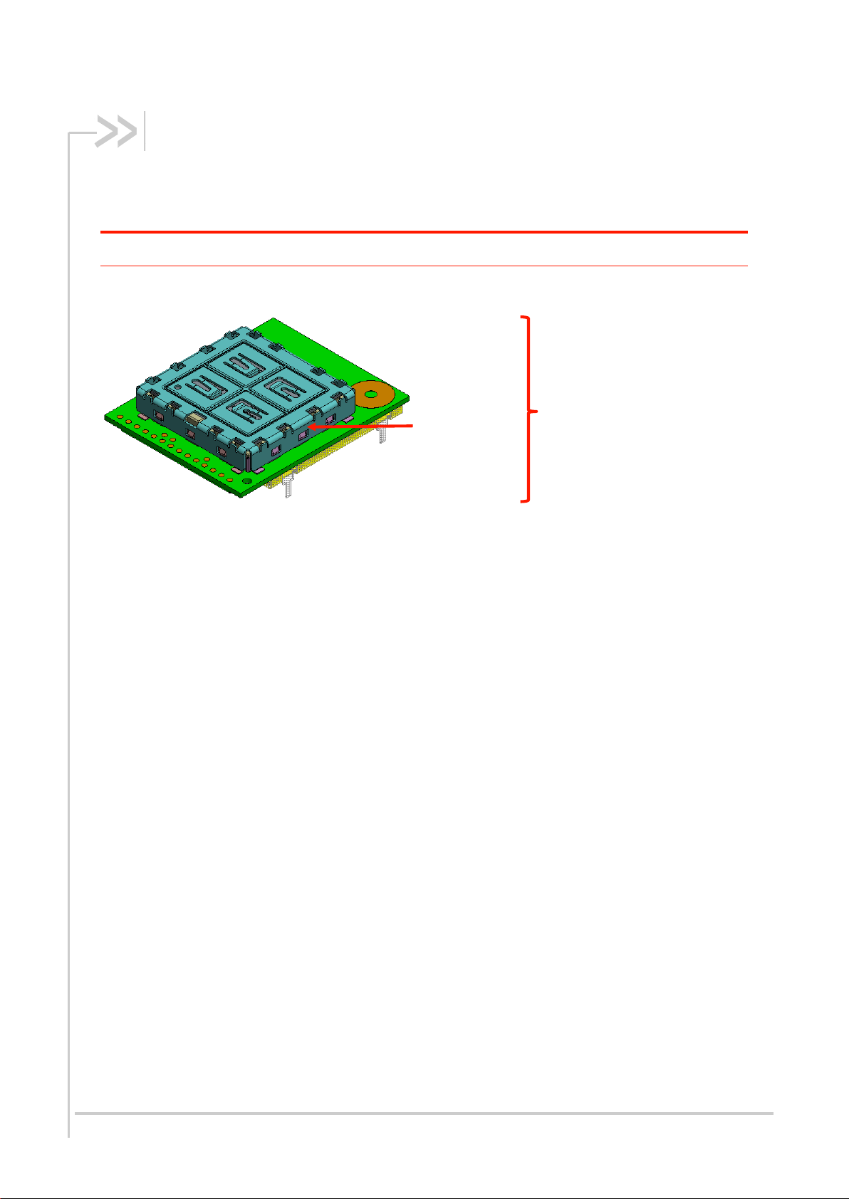
1. Introduction
Snap-in Socket
with a cover
Q26 Carrier Board
The AirPrime Q26 Carrier Board is used to provide an interface between applications using an
AirPrime Q26 (which includes Q2686, Q2687, Q2686 Refreshed, Q2687 Refreshed and Q2698) form
factor and the AirPrime HL6528, HL6528RD or HL8548 embedded module.
Note: HL6528 and HL6528RD refer to 1.8V variants of the HL6. 2.8V variants (which are not supported by
the Q26 Carrier Board) are designated as HL6528-2.8V and HL6528RD-2.8V.
AirPrime HL modules are inserted in a Snap-in Socket which is mounted on a PCB to form the Q26
Carrier Board.
Figure 1. Q26 Carrier Board
This document describes how the Q26 Carrier Board enables applications to change from using a
Q26 module to an HL6528, HL6528RD or HL8548 module, as well as provides schematic diagrams
and mechanical details to facilitate the user’s understanding and configuration of the Q26 Carrier
Board.
The current Q26 Carrier Board is compatible with the following AirPrime HL modules:
HL6528
HL6528RD
HL8548
For simplicity, these three modules will be collectively referred to as “HL6 and HL8 modules”
throughout this document.
Likewise, the Q2686, Q2687, Q2686 Refreshed, Q2687 Refreshed will be collectively referred to as
“Q268xx”, AirPrime Q26 variants as “Q26”, and the Q26 Carrier Board to “Q26CB” in this document.
For more information regarding AirPrime Q26, and HL6 and HL8 modules, refer to the specific product
technical specifications listed in section 7.1 Reference Documents.
4117783 Rev 6.0 December 19, 2016 9
Page 10
2. General Description
Dimension
Q268xx
Q2698
Q26 Carrier Board*
Length
40 mm
40 mm
40 mm
Width
32.2 mm
32.2 mm
32.2 mm
Thickness
4.0 mm
6.2 mm
8.9 mm
Board-to-board stack up height
3.0 mm
3.0 mm
3.0 mm
Weight
8 g
11.8 g
12 g
Module
Vmin
Vnom
Vmax
Q268xx
3.2 V
3.6 V
4.8 V
Q2698
3.4 V
3.8 V
4.2 V
HL6528
3.2 V
3.7 V
4.5 V
HL6528RD
3.35 V
3.7 V
4.3 V
HL8548
3.2 V
3.7 V
4.5 V
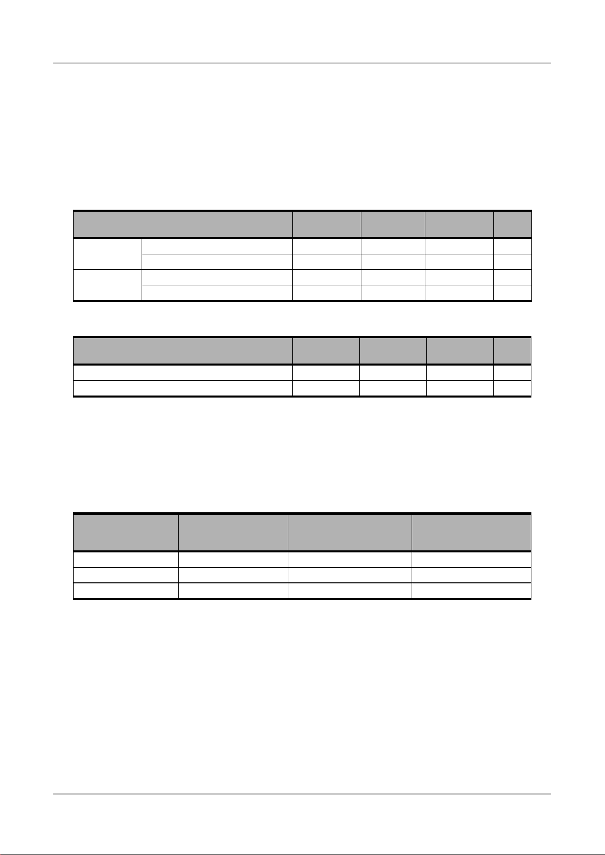
2.1. Physical Dimension
The following table shows the physical dimension of the Q26 module and the Q26 Carrier Board.
Table 1. Physical Dimension
* Dimensions listed do not include shielding pins.
The Q26 Carrier Board can be assembled to any existing Q26 product design without the need for
any additional setup or configuration.
2.2. Operating Voltage
Refer to the following table for the operating voltages of the Q26, and the HL6 and HL8 modules.
Table 2. Operating Voltage
Note: Take note of the difference between voltage ranges when using the Q26 Carrier Board on an
existing Q26 application.
4117783 Rev 6.0 December 19, 2016 10
Page 11
User Guide
General Description
Parameter
Minimum
Typical
Maximum
Unit
VCC_2V8
Output voltage
2.74
2.8
2.86
V
Output current
15
mA
VCC_1V8
Output voltage
1.76
1.8
1.94
V
Output current
15
mA
Parameter
Minimum
Typical
Maximum
Unit
Output voltage
1.7
1.8
1.9 V Output current
50
mA
Condition
Q26
Q26 Carrier Board with
HL6528, HL6528RD
Q26 Carrier Board
with HL8548
Operating/Class A
-30°C to +70°C
-30°C to +70°C
-30°C to +70°C
Operating/Class B
-40°C to +85°C
-40°C to +80°C
-40°C to +75°C
Storage
-40°C to 85°C
-40°C to +85°C
-40°C to +85°C
2.3. Power Supply Output
The power supply output can be used to pull up signals such as IOs, as well as act as a voltage
references for the ADC interface.
The Q26 modules have two digital power supply outputs – VCC_2V8 (pin 10) and VCC_1V8 (pin 5);
while the HL6 and HL8 modules only have one – VGPIO (pin 45). Refer to the tables below for more
information.
Table 3. VCC_2V8 and VCC_1V8 on the Q26 Modules
Table 4. VGPIO on the HL6 and HL8 Modules
2.4. Operating Temperature
The Q26 Carrier Board is an industrial-grade device and has the following operating temperature
range.
Table 5. Operating Temperature
4117783 Rev 6.0 December 19, 2016 11
Page 12
User Guide
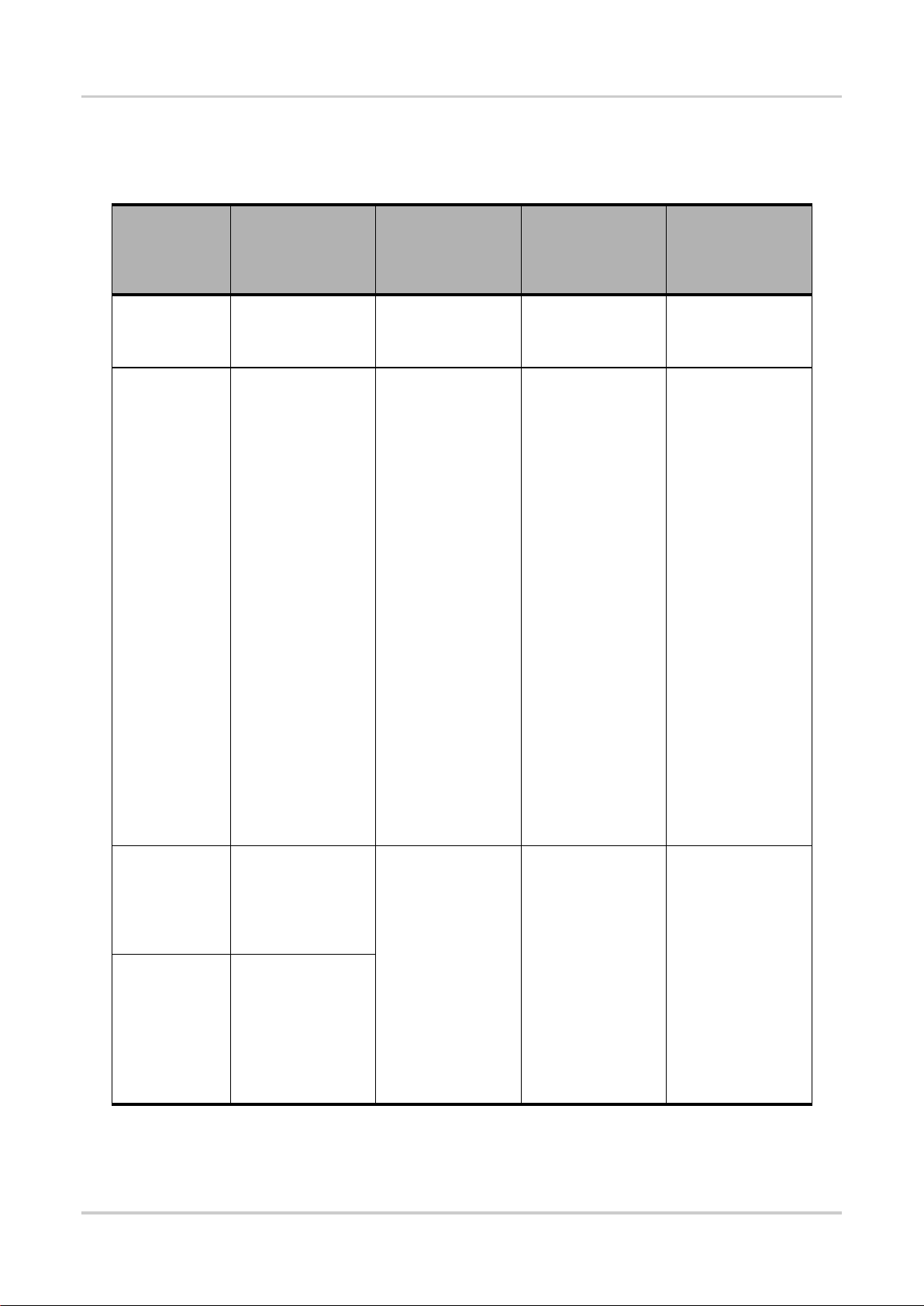
General Description
Feature
Q268xx
Q2698
Q26 Carrier
Board with
HL6528,
HL6528RD
Q26 Carrier
Board with
HL8548
Shielding
The Q268xx
embedded module
has complete body
shielding.
The Q2698
embedded module
has complete body
shielding.
Complete body
shielding (Q26
Carrier Board and
HL module)
Complete body
shielding (Q26
Carrier Board and
HL module)
Application
interface
Full set of AT
commands for
GSM/GPRS/EG
PRS including
GSM 07.07 and
07.05 AT
command sets
Status indication
for GSM
Full set of AT
commands for
GSM/GPRS/EG
PRS including
GSM 07.07 and
07.05 AT
command sets
Status indication
for GSM
Full set of AT
commands for
GSM/GPRS
including GSM
07.07 and 07.05
AT command
sets
Comprehensive
set of dedicated
AT commands
for M2M
applications
NDIS NIC
interface
support
(Windows XP,
Windows 7,
Windows 8,
Windows CE,
Linux)
Multiple non-
multiplexed
USB channel
support
Dial-up
networking
USB selective
suspend to
maximize power
savings
CMUX
multiplexing
over UART
AT command
interface –
3GPP 27.007
standard, plus
proprietary
extended AT
commands
GSM/DCS
Output Power
Class 4 (2 W)
for GSM 850
and E-GSM
Class 1 (1 W)
for DCS and
PCS
Quad-Band
GSM GPRS
EDGE
850/900/1800/1
900 MHz
GPRS class 12
EDGE (E-
GPRS) multislot class 12
Class 4 (2 W)
for GSM 850
and E-GSM
Class 1 (1 W)
for DCS and
PCS
Quad-band
GSM850/EGSM/DCS/PCS
GPRS Multi-slot
class 10
R99 support
PBCCH support
Quad-band GSM /
GPRS / EDGE (850
MHz, 900 MHz,
1800 MHz, 1900
MHz)
GPRS
GPRS multislot
class 10
Multislot class 2
supported
PBCCH support
Coding
schemes: CS1
to CS4
2.5. General Features
Table 6. General Features
4117783 Rev 6.0 December 19, 2016 12
Page 13

User Guide
General Description
Feature
Q268xx
Q2698
Q26 Carrier
Board with
HL6528,
HL6528RD
Q26 Carrier
Board with
HL8548
EGPRS
EGPRS
multislot class
10
Multislot class 2
supported
PBCCH support
Coding
schemes MCS1
to MCS9
Coding
schemes:
CS1 to CS4
(GPRS)
MCS 5 to
MCS 9
(EDGE)
3G
Penta-Band
UMTS/HSPA
(WCDMA/FDD)
2100/1900/850/800/
900 MHz (band I, II,
V, VI, VIII):
Downlink data
rates up to
HSDPA
Category 10
(14.4 Mbps)
Uplink data
rates up to
HSUPA
Category 6
(5.76 Mbps)
Hexa-band UMTS
WCDMA FDD (800
MHz (B19), 850
MHz (B5/B6), 900
MHz (B8), 1900
MHz (B2), 2100
MHz (B1))
Voice
GSM Voice
Features with
Emergency calls
118 XXX
Full Rate (FR),
Enhanced Full
Rate (EFR),
Half Rate (HR)
and Adaptive
Multi-rate (AMR)
Echo
cancellation and
noise reduction
Full duplex
Hands free
Half Rate (HR),
Full Rate (FR)
and Enhanced
Full Rate (EFR)
and Adaptive
multi-rate (AMR)
Echo
cancellation and
noise reduction
Hands free
Analog and
Digital
interfaces
Supports Full
Rate (FR),
Enhanced Full
Rate (EFR),
Half Rate (HR)
and Adaptive
Multi-rate (AMR)
Noise reduction
and echo
cancellation
DTMF
generation
Digital interface
(ONLY)
Supports
Enhanced Full
Rate (EFR), Full
Rate (FR), Half
Rate (HR), and
both NarrowBand and Wideband Adaptive
Multi-rate (AMRNB and AMRWB) vocoders
MO and MT
calling
Echo
cancellation and
noise reduction
Emergency calls
(112, 110, 911,
etc.)
Incoming call
notification
DTMF
generation
4117783 Rev 6.0 December 19, 2016 13
Page 14

User Guide
General Description
Feature
Q268xx
Q2698
Q26 Carrier
Board with
HL6528,
HL6528RD
Q26 Carrier
Board with
HL8548
SMS
SMS MT, MO
SMS CB
SMS storage
into SIM card
SMS MT, MO
SMS CB
SMS storage
into SIM card
SMS class 0,1
and 2
SMS MT, MO
SMS storage
into SIM card or
Flash memory
Concatenation
of MT SMS
SMS MT, MO
CS and PS
support
SMS saving to
SIM card or ME
storage
SMS reading
from SIM card
or ME storage
SMS sorting
SMS
concatenation
SMS Status
Report
SMS
replacement
support
SMS storing
rules (support of
AT+CNMI,
AT+CNMA)
GSM
Supplementary
Services
Call Forwarding,
Call Barring
Multiparty
Call Waiting,
Call Hold
USSD
Call Forwarding,
Call Barring
Multiparty
Call Waiting,
Call Hold
USSD
Call Forwarding
Call Barring
Multiparty
Service
Call Waiting
Call Hold
USSD
Automatic
answer
Call Barring
Call Forwarding
Call Hold
Caller ID
Call Waiting
Multi-party
service
USSD
Automatic
answer
Data/Fax
Data circuit
asynchronous,
transparent, and
non-transparent
up to 14400
bits/s
Fax Group 3
compatible
Data and fax not
supported
Data circuit
asynchronous nontransparent at 9600
bits/s
Circuit switched
data at 9600 bits/s
4117783 Rev 6.0 December 19, 2016 14
Page 15

User Guide
General Description
Feature
Q268xx
Q2698
Q26 Carrier
Board with
HL6528,
HL6528RD
Q26 Carrier
Board with
HL8548
SIM Interface
1.8V/3V SIM
interface
5V SIM
interfaces are
available with
external
adaptation
SIM Tool Kit
Release 99
1.8V/3V USIM
interface
Dual SIM Dual
Standby support
1.8V/3.0V
support for
SIM1
3V interface for
SIM2
Hot plug and hot
extraction
detection (SIM1
only)
Supports SIM
application tool
kit with
proactive SIM
commands
Dual SIM Single
Standby with
fast network
switching
capability
1.8V/3V support
SIM extraction /
hot plug
detection
SIM/USIM
support
Conforms with
ETSI UICC
Specifications.
Supports SIM
application tool
kit with
proactive SIM
commands
Real Time
Clock
Real Time Clock
(RTC) with calendar
and alarm
Real Time Clock
(RTC) with calendar
and alarm
Real Time Clock
(RTC) with calendar
and alarm
Real Time Clock
(RTC) with calendar
and alarm
Temperature
Sensor
Temperature
monitoring
Alarms
Temperature
monitoring
Alarms
Temperature
monitoring
Alarms
Temperature
monitoring
Alarms
Interface
Q26 Carrier Board with
HL6528, HL6528RD
Q26 Carrier Board with
HL8548
Power Supply
Digital section running under 2.8V and 1.8V
3V/1V8 SIM Interface
Main Serial Link
Auxiliary Serial Link
2.6. Interfaces
The following table enumerates the interfaces available on the Q26 modules and indicates whether
these interfaces are also available on the HL6 and HL8 modules.
The table is marked with the following indicators:
: Fully supported
: Partially supported or with specific behavior
: Not supported
Compatibility details are described in section 4 Features Configuration and Limitations.
Table 7. Interface Compatibility
4117783 Rev 6.0 December 19, 2016 15
Page 16

User Guide
General Description
Interface
Q26 Carrier Board with
HL6528, HL6528RD
Q26 Carrier Board with
HL8548
Analog Audio
Digital Audio (PCM)
USB 2.0
* General Purpose IO
Keyboard
Serial Interface (SPI)
Parallel Interface
RF Interface
ADC
PWM/Buzzer Output
Backup Battery (BAT_RTC)
Battery Charging Interface
External Interrupt
JTAG
RF Interface
LED0 Signal
Q26 Carrier Board
Test Point Number
Signal Name
Group Designation
Remark
TP202
VBATT
Power
TP245
V_GPIO
TP205
VCC_1V8
TP277
GND
TP219
ON-OFF
ON/OFF Signal
TP218
\RESET
TP252
USB-VBUS
USB
Only supported with an
HL8548 modules
TP254
USB_D+
TP256
USB_D-
TP272
UART_RTS
UART
TP271
UART_TXD
TP276
UART_DTR
TP275
UART_CTS
TP273
UART_RXD
TP270
UART_DCD
TP274
UART_DSR
* The HL6528RD supports USB 2.0; while the HL6528 does not.
2.7. Test Points
The following table describes the 20 test points available for customer use on the Q26 Carrier Board.
Locations of these 20 test points are shown in Figure 2 Test Point Locations below.
Table 8. Test Points
4117783 Rev 6.0 December 19, 2016 16
Page 17

User Guide
General Description
Q26 Carrier Board
Test Point Number
Signal Name
Group Designation
Remark
TP278
SP1_SRDY
Debug
Only supported with an
HL6528 and HL6528RD
module
Figure 2. Test Point Locations
4117783 Rev 6.0 December 19, 2016 17
Page 18

3. Pin Mapping
CN301
Pin #
Q268xx Signal Name
Q2698 Signal Name
Q26 Carrier Board with
HL6528, HL6528RD
Signal Name
Q26 Carrier Board with
HL8548 Signal Name
Compatibility Notes
1
ADC0/VBATT
ADC0/VBATT
VBATT_PA
VBATT_PA
2
ADC0/VBATT
ADC0/VBATT
VBATT_PA
VBATT_PA
3
ADC0/VBATT
ADC0/VBATT
VBATT
VBATT
4 ADC0/VBATT
ADC0/VBATT
VBATT
VBATT
5
VCC_1V8
VCC_1V8
VGPIO
VGPIO
6 CHG-IN
CHG-IN
- - Not supported
7
BAT-RTC
BAT-RTC
BAT_RTC
BAT_RTC
The HL8548 supports a
different voltage range
8
CHG-IN
CHG-IN
- - Not supported
9
SIM-VCC
SIM-VCC
UIM1_VCC
UIM1_VCC
10
VCC_2V8
VCC_2V8
- -
11
SIM-IO
SIM-IO
UIM1_DATA
UIM1_DATA
12
SIMPRES
SIMPRES/GPIO18
UIM1_DET/GPIO3
GPIO3 / UIM1_DET
13
~SIM-RST
~SIM-RST
UIM1_RESET
UIM1_RESET
14
SIM-CLK
SIM-CLK
UIM1_CLK
UIM1_CLK
15
BUZZER0
BUZZER0
UIM2_RESET/BUZZER
PWM1
The following table lists the pin assignment mapping of the Q26 Carrier Board and the HL6528, HL6528RD and HL8548 modules (which are inserted in the
Snap-in Socket on the Carrier Board); as well as indicates restrictions or limitations on the signals/pins, if any.
The pin number specified in the table below refers to the corresponding pin number on the board-to-board connector (CN301) of the Q26 Carrier Board, while
signal names refer to the module’s signal name. For more information about module signal names, refer to the product technical specifications listed in
section 7.1 Reference Documents.
Table 9. Pin Mapping
4117783 Rev 6.0 December 19, 2016 18
Page 19

User Guide
Pin Mapping
CN301
Pin #
Q268xx Signal Name
Q2698 Signal Name
Q26 Carrier Board with
HL6528, HL6528RD
Signal Name
Q26 Carrier Board with
HL8548 Signal Name
Compatibility Notes
16
BOOT
BOOT
TP1
TP1 17
LED0
LED0
- - Not supported
18
~RESET
~RESET
RESET_IN
RESET_IN_N
19
ON/~OFF
ON/~OFF
PWR_ON
PWR_ON_N
20
ADC1/BAT-TEMP
ADC1/BAT-TEMP
ADC0
ADC0
The HL modules support a
different voltage range
21
ADC2
ADC2
ADC1
ADC1
The HL modules support a
different voltage range
22
GPIO31/SPI1-LOAD
GPIO31/SPI1-Load
- - Not supported
23
SPI1-CLK/GPIO28
SPI1-CLK/GPIO28
- - Not supported
24
SPI1-I/GPIO30
SPI1-I/GPIO30
- - Not supported
25
SPI1-IO/GPIO29
SPI1-IO/GPIO29
- - Not supported
26
SPI2-CLK/GPIO32
SPI2-CLK/GPIO32
GPIO7
GPIO7
27
SPI2-IO/GPIO33
SPI2-IO/GPIO33
GPIO8
GPIO8
28
GPIO35/SPI2-Load
GPIO35/SPI2-Load
GPIO6
GPIO6
29
SPI2-I/GPIO34
SPI2-I/GPIO34
UIM2_DET/GPIO4
GPIO4
30
CT104-RXD2/GPIO15/INT4
CT104-RXD2/GPIO15/INT4
- - Not supported
31
CT103-TXD2/GPIO14
CT103-TXD2/GPIO14
- - Not supported
32
~CT106-CTS2/GPIO16
~CT106-CTS2/GPIO16
- - Not supported
33
~CT105-RTS2/GPIO17
~CT105-RTS2/GPIO17
- - Not supported
34
MIC2N
MIC2N
MIC_N
NC
Only supported in the HL6528
35
SPK1P
SPK1P
SPKR_P
NC
Only supported in the HL6528
36
MIC2P
MIC2P
MIC_P
NC
Only supported in the HL6528
37
SPK1N
SPK1N
SPKR_N
NC
Only supported in the HL6528
38
MIC1N
MIC1N
MIC_N
NC
Only supported in the HL6528
39
SPK2P
SPK2P
SPKR_P
NC
Only supported in the HL6528
4117783 Rev 6.0 December 19, 2016 19
Page 20

User Guide
Pin Mapping
CN301
Pin #
Q268xx Signal Name
Q2698 Signal Name
Q26 Carrier Board with
HL6528, HL6528RD
Signal Name
Q26 Carrier Board with
HL8548 Signal Name
Compatibility Notes
40
MIC1P
MIC1P
MIC_P
NC
Only supported in the HL6528
41
SPK2N
SPK2N
SPKR_N
NC
Only supported in the HL6528
42
A1*/Reserved
Reserved
- - Not supported
43
GPIO0/32kHz
GPIO0/32kHz
NC
32K_CLKOUT
Not supported in the HL6528
44
SCL1/GPIO26
SCL1/GPIO26
- - Not supported
45
GPIO19
GPIO19
GPIO2/UIM2_VCC_CTRL
GPIO2
46
SDA1/GPIO27
SDA1/GPIO27
- - Not supported
47
GPIO21
GPIO21
UIM2_CLK/PWM
PWM2/GPIO12
Not supported in the HL6528
48
GPIO20
GPIO20
GPIO1/I2C_CLK
GPIO1/I2C_CLK
49
INT1/GPIO25
INT1/GPIO25
- - Not supported
50
INT0/GPIO3
INT0/GPIO3
- - Not supported
51
GPIO1/A25/~CS2*
GPIO1
GPIO5/I2C_DATA
GPIO5/I2C_SDA
52
VPAD-USB
VPAD-USB
NC
USB_VBUS
Not supported in the HL6528
53
GPIO2/A24*
GPIO2
SPI1_MRDY
DEBUG_RX
54
USB-DP
USB-DP
NC
USB_D+
Only supported in the HL8548
55
GPIO23
GPIO23
SPI1_CLK
GPIO11
Not supported in the HL6528
56
USB-DM
USB-DM
NC
USB_D-
Only supported in the HL8548
57
GPIO22
GPIO22
SPI1_MISO
GPIO10
Not supported in the HL6528
58
GPIO24
GPIO24
SPI1_MOSI
GPIO15
Not supported in the HL6528
59
COL0/GPIO4
COL0/GPIO4
- - Not supported
60
COL1/GPIO5
COL1/GPIO5
- - Not supported
61
COL2/GPIO6
COL2/GPIO6
- - Not supported
62
COL3/GPIO7
COL3/GPIO7
- - Not supported
63
COL4/GPIO8
COL4/GPIO8
- - Not supported
64
ROW4/GPIO13
ROW4/GPIO13
- - Not supported
65
ROW3/GPIO12
ROW3/GPIO12
- - Not supported
4117783 Rev 6.0 December 19, 2016 20
Page 21

User Guide
Pin Mapping
CN301
Pin #
Q268xx Signal Name
Q2698 Signal Name
Q26 Carrier Board with
HL6528, HL6528RD
Signal Name
Q26 Carrier Board with
HL8548 Signal Name
Compatibility Notes
66
ROW2/GPIO11
ROW2/GPIO11
- - Not supported
67
ROW1/GPIO10
ROW1/GPIO10
- - Not supported
68
ROW0/GPIO9
ROW0/GPIO9
- - Not supported
69
~CT125-RI/GPIO42
~CT125-RI/GPIO42
UART1_RI
UART1_RI
70
~CT109-DCD1/GPIO43
~CT109-DCD1/GPIO43
UART1_DCD
UART1_DCD
71
CT103-TXD1/GPIO36
CT103-TXD1/GPIO36
UART1_TX
UART1_TX
72
~CT105-RTS1/GPIO38
~CT105-RTS1/GPIO38
UART1_RTS
UART1_RTS
73
CT104-RXD1/GPIO37/INT2
CT104-RXD1/GPIO37/INT2
UART1_RX
UART1_RX
74
~CT107-DSR1/GPIO40
~CT107-DSR1/GPIO40
UART1_DSR
UART1_DSR
75
~CT106-CTS1/GPIO39
~CT106-CTS1/GPIO39
UART1_CTS
UART1_CTS
76
~CT108-2-DTR1/GPIO41/INT3
~CT108-2-DTR1/GPIO41/INT3
UART1_DTR
UART1_DTR
77
PCM-SYNC
PCM-SYNC
PCM_SYNC
PCM_SYNC
78
PCM-IN
PCM-IN
PCM_IN
PCM_IN
79
PCM-CLK
PCM-CLK
PCM_CLK
PCM_CLK
80
PCM-OUT
PCM-OUT
PCM_OUT
PCM_OUT
81
/OE-R/W*/Reserved
Reserved
- - Not supported
82
DAC0*/Reserved
Reserved
- - Not supported
83
/CS3*/Reserved
Reserved
- - Not supported
84
/WE-E*/Reserved
Reserved
- - Not supported
85
D0*/Reserved
Reserved
- - Not supported
86
D15*/Reserved
Reserved
- - Not supported
87
D1*/Reserved
Reserved
- - Not supported
88
D14*/Reserved
Reserved
- - Not supported
89
D2*/Reserved
Reserved
- - Not supported
90
D13*/Reserved
Reserved
- - Not supported
91
D3*/Reserved
Reserved
- - Not supported
4117783 Rev 6.0 December 19, 2016 21
Page 22

User Guide
Pin Mapping
CN301
Pin #
Q268xx Signal Name
Q2698 Signal Name
Q26 Carrier Board with
HL6528, HL6528RD
Signal Name
Q26 Carrier Board with
HL8548 Signal Name
Compatibility Notes
92
D12*/Reserved
Reserved
- - Not supported
93
D4*/Reserved
Reserved
- - Not supported
94
D11*/Reserved
Reserved
- - Not supported
95
D5*/Reserved
Reserved
- - Not supported
96
D10*/Reserved
Reserved
- - Not supported
97
D6*/Reserved
Reserved
- - Not supported
98
D9*/Reserved
Reserved
- - Not supported
99
D7*/Reserved
Reserved
- - Not supported
100
D8*/Reserved
Reserved
- - Not supported
* This signal is only available on the Q2687.
4117783 Rev 6.0 December 19, 2016 22
Page 23

4. Features Configuration and
Q26
Q26 Carrier Board with
HL6528, HL6528RD
Q26 Carrier Board with
HL8548
Pin #
Signal Name
Voltage
Signal Name*
Signal Name*
26
GPIO32
2.8V
GPIO7
GPIO7
27
GPIO33
2.8V
GPIO8
GPIO8
28
GPIO35
2.8V
GPIO6
GPIO6
29
GPIO34
2.8V
GPIO4
GPIO4
43
GPIO0/32kHz
2.8V
-
32K_CLKOUT
45
GPIO19
2.8V
GPIO2
GPIO2
47
GPIO21
2.8V
UIM2_CLK/PWM2**
GPIO12
48
GPIO20
2.8V
GPIO1
GPIO1
51
GPIO1
1.8V
GPIO5
GPIO5
53
GPIO2
1.8V
SPI_MRDY**
DEBUG_RX**
55
GPIO23
2.8V
SPI_CLK**
GPIO11
57
GPIO22
2.8V
SPI_MISO**
GPIO10
58
GPIO24
2.8V
SPI_MOSI**
GPIO15
12
GPIO18/SIMPRES
1.8V
GPIO3/UIM1_DET
GPIO3/UIM1_DET
Limitations
The following sub-sections describes the adjustments or configuration needed to ensure full
compatibility when using the Q26 Carrier Board in an existing design.
4.1. Hardware Features
4.1.1. Antenna
The Q26 Carrier Board only supports UFL/SMA and RF pad antenna connectors; it does not support
Precidip antenna connectors.
4.1.2. General Purpose Input/Output
The Q26 modules support up to 44 GPIOs; however, the Q26 Carrier Board has limited GPIO support
due to the HL6 and HL8 modules having less GPIOs (the HL6528 and HL6528RD modules only
support 8, while the HL8548 module supports 12).
Table 10. Compatible GPIOs
* HL embedded module signal name. For more information about HL signal names, refer to the product technical
** This signal is an extended function and can’t be used as a GPIO.
4117783 Rev 6.0 December 19, 2016 23
specifications listed in section 7.1 Reference Documents.
Page 24

User Guide
Features Configuration and Limitations
Additionally, all HL6 and HL8 GPIOs have an output voltage of 1.8 V. To compensate for this, level
shifters are incorporated into the Q26 Carrier Board to match the Q26 module’s GPIO output voltage.
The level shifter used in the Q26 Carrier Board contains an auto-sense translator which quickly
transforms an input driver to an output driver and vice versa. The input driver to the auto-sense
translator should be capable of driving 2 mA of peak output current for proper operation. Note that
although the peak current from the input signal is relatively large, the average current is small and
consistent with a standard CMOS input stage.
4.1.3. Serial Interface
Q26 modules support two serial interfaces – SPI and I2C. However, both serial interfaces are
controlled by the Open AT Application Framework which is not supported by the HL6 and HL8
modules; SPI and I2C buses are not supported in the Q26 Carrier Board.
4.1.4. Parallel Interface
The parallel interface of the Q26 is controlled by the Open AT Application Framework, which is not
supported by the HL6 and HL8 modules; parallel interface is not supported in the Q26 Carrier Board.
4.1.5. Keyboard Interface
The keyboard interface of the Q26 is controlled by the Open AT Application Framework, which is not
supported by the HL6 and HL8 modules; keyboard interface is not supported in the Q26 Carrier
Board.
4.1.6. Main Serial Link (UART1)
The main serial link (UART1) is used for communication between the Q26 Carrier board and a PC or
host processor. It consists of a flexible 8-wire serial interface that complies with the RS-232 interface.
The UART1 voltage level of the HL6 and HL8 modules (1.8 V) is different from that of the Q26
modules (2.8 V). To ensure that UART is fully compatible, an 8-bit voltage level shifter is added in the
Q26 Carrier Board to match the Q26 module’s 2.8 V voltage and also remain 3.3 V tolerant.
4.1.7. Auxiliary Serial Link (UART2)
Although Q26 modules support an auxiliary serial link (UART2) interface, this interface is not
supported by the HL6 and HL8 modules and so is also not supported in the Q26 Carrier Board.
4.1.8. SIM Interface
A fully compatible 1.8V and 3V SIM card interface is available on the Q26 Carrier Board.
4117783 Rev 6.0 December 19, 2016 24
Page 25

User Guide
Features Configuration and Limitations
4.1.9. USB 2.0
A 4-wire USB slave interface is available on the Q26 modules that comply with USB 2.0 protocol
signaling, but not with the electrical interface due to the 5V interface of VPAD-USB. The VPAD-USB
of the Q26 is 3V3 so an extra regulator is needed on the application. However, the USB VBUS of the
HL6528RD and HL8548 modules is 5V, which is directly compatible to the USB interface. The extra
regulator on the Q26 application should be removed when using the Q26 Carrier Board.
Caution: Due to the difference in USB speeds between the Q26 and the HL modules, it is recommended that
a low capacitance (0.5 pF) ESD diode be used in the application USB port.
Note: The HL6528 does not support USB.
4.1.10. Audio
4.1.10.1. Analog Audio
The Q26 Carrier Board can only support the use of one analog audio interface (MIC1/MIC2 and
SPK1/SPK2). If the existing Q26 application uses an external single-ended MIC, the external bias
circuitry must be removed when using the Q26 Carrier Board because the HL6528 and HL6528RD
already includes a built-in internal bias voltage; the HL8548 does not support analog audio.
Note: Sierra Wireless does not recommend using single-ended audio as the DTMF noise floor is typically
high when using the Q26 Carrier Board.
4.1.10.2. Digital Audio (PCM)
The digital audio output of the HL8548 is electrically compatible with Q26 modules; however, the
HL6528 and HL6528RD have a 2.8 V PCM output so an internal level shifter is reserved as an option
when using the Q26 Carrier Board with an HL6528 or HL6528RD module.
For details about PCM protocol, refer to the product technical specification of the corresponding HL6
or HL8 embedded module in section 7.1 Reference Documents.
4.1.11. RF Performance
The Q26 Carrier Board's RF performance meets with 3GPP specifications when equipped with an
HL6528 or an HL6528RD. However, when equipped with an HL8548, the Q26 Carrier Board has the
following exceptions to 3GPP specifications:
1. RX sensitivity deviates in specific channels of 2G bands (channel 202 of the GSM850 band,
channel 5 of the GSM900 band, channel 846 of the DCS band and channel 741 of the PCS
band).
2. RX sensitivity deviates in specific channels of 3G bands (channels 10625 to 10670 of Band 1,
channels 9875 to 9885 of Band 2, and channels 2975 to 2980 of Band 8).
4.1.12. Battery Charging Interface
Battery charging function is not supported in the Q26 Carrier Board.
4117783 Rev 6.0 December 19, 2016 25
Page 26

User Guide
Features Configuration and Limitations
Condition
Q268xx
Q2698
Q26 Carrier Board with
HL6528, HL6528RD
Q26 Carrier Board
with HL8548
ADC1/BAT-TEMP
0 – 2 V
0 – 4 V
0 – 3 V (TBC)
0 – 1.2 V (TBC)
ADC2
0 – 2 V
0 – 4 V
0 – 3 V (TBC)
0 – 1.2 V (TBC)
4.1.13. Power ON Signal
The HL6 and HL8 modules have an active low power ON signal pin, while Q26 modules have an
active high power ON signal. An inverter is added to the Q26 Carrier Board to reverse the polarity of
the signal.
4.1.14. Reset Signal
When using the Q26 Carrier Board, a low level pulse must be sent on the reset pin for 10 ms. This
action will immediately restart the AirPrime HL6 or HL8 module with the PWR_ON_N signal at low
level.
4.1.15. BOOT Signal
Because the BOOT pin is connected to VCC_1V8 in the Q268xx (the Q2698 does not have a BOOT
pin), and set to active low, the BOOT signal has to be reversed when using the Q26 Carrier Board.
4.1.16. ADC
Two Analog to Digital converter inputs, ADC1/BAT-TEMP and ADC2 are available when using the
Q26 Carrier Board. These converters are 10-bit resolution ADCs with voltage range shown in the
table below.
Table 11. ADC Voltage Range
Because the HL8548 voltage range is narrower than the Q26 input range, if an HL8548 module is
used in the Q26 Carrier Board and receives an input voltage of more than 1.2 V, the ADC port might
be damaged. To protect the Q26 Carrier Board from overvoltage input, additional circuitry has been
added to the carrier board.
Similarly, the HL6528 and HL6528RD voltage range is also narrower than the Q2698 input range and
additional circuitry on the Q26 Carrier Board protects it from overvoltage when migrating from an
application that uses a Q2698.
However, if the existing application uses a Q268xx module, using an HL6528 or HL6528RD module
with the Q26 Carrier Board might not provide enough resolution as the voltage range of the HL6 is
wider than that of the Q268xx.
4117783 Rev 6.0 December 19, 2016 26
Page 27

User Guide
Features Configuration and Limitations
Parameter
Q26
Q26 Carrier Board with
HL6528, HL6528RD
Q26 Carrier Board with
HL8548
Min
Typ
Max
Min
Typ
Max
Min
Typ
Max
Input Voltage
1.85 V
-
3 V - 3 V - 1.0 V
1.8 V
1.9 V
Input current
consumption
3.0 µA
3.3 µA
3.6 µA
-
2.5 µA
- - 1 µA
-
Output Voltage
2.40 V
2.45 V
2.50 V
2.82 V
3.0 V
3.18 V
1.71 V
1.8 V
1.89 V
Output current
- - 2 mA
-
0.6 mA
- - 25 mA
-
Q26
Q26 Carrier Board with
HL6528, HL6528RD
Q26 Carrier Board with
HL8548
Pin #
Signal Name
Signal Name
Signal Name
53
GPIO2
SPI1_MRDY
DEBUG_RX
55
GPIO23
SPI1_CLK
57
GPIO22
SPI1_MISO
58
GPIO24
SPI1_MOSI
4.1.17. BAT_RTC
As shown in the table below, the voltage range varies between Q26 modules, and the HL6 and HL8
modules. Additional circuitry has been added on the Q26 Carrier Board to protect it from overvoltage
input.
Table 12. BAT_RTC
Note: The HL6528 and HL6528RD output is higher than the Q26.
The HL8548 output is only 1.8 V (typical) which might not be enough to charge the application’s
battery.
4.1.18. Debug Port
HL6 and HL8 embedded modules support a software trace interface that provides real-time instruction
and data trace of the modem core.
The following table provides the pin mapping of the debug port between the Q26 Carrier Board and
the HL6 and HL8 embedded modules.
Table 13. Debug Port
In addition to the pins specified in the table above, the Q26 Carrier Board also has a test pad, TP278,
which corresponds to pin 44 of the HL6 and HL8 module (SPI1_SRDY on the HL6528 and
HL6528RD, DEBUG_TX on the HL8548) which is also used for debug.
4117783 Rev 6.0 December 19, 2016 27
Page 28

User Guide
Features Configuration and Limitations
Q26 Carrier Board with HL6528, HL6528RD
Q26 Carrier Board with HL8548
R336, R337
R301, R313, R322, R323 (default configuration)
4.2. Optional Pad Configuration
4.2.1. PCM Voltage Level Shifter Selection
Because the voltage level output of the PCM varies between the HL6528, HL6528RD and HL8548
(with the HL6528 and HL6528RD having 2.8 V, and the HL8548 having 1.8 V), optional component
configuration is made available in the Q26 Carrier Board.
The Q26 Carrier Board’s PCM interface is configured to use HL8548 (1.8 V) by default. When using
an HL6528 or HL6528RD module, resistors R301, R313, R322 and R323 must be removed and
resistors R336 and R337 installed if PCM is to be used. Otherwise, PCM should be turned and kept
off when using an HL6528 or HL6528RD module to prevent the application’s PCM codec from being
damaged with an incorrect carrier board configuration.
Note: Ensure that the module used in the Q26 Carrier Board is compatible with the carrier board’s PCM
configuration. Using a module with the incorrect carrier board configuration will damage the
customer’s PCM application.
Table 14. Optional Component Configuration for PCM
Figure 3. PCM Voltage Level Shifter
Figure 4. Optional Components Placement
4117783 Rev 6.0 December 19, 2016 28
Page 29

User Guide
Features Configuration and Limitations
LED0
By Default
R305
0R
4.2.2. LED0
FLASH-LED indicates the GSM activity status of the modules inside the Snap-in Socket on the Q26
Carrier Board and can also be used to drive an LED. Application designers have the option of
selecting to use GPIO4 for concurrent common GPIO use and FLASH-LED.
By default, R305 is connected on the Q26 Carrier Board to allow GPIO4 to be used as a regular GPIO
and LED0 at the same time.
Refer to command +KSYNC in document [7] AirPrime HL6 and HL8 Series AT Commands Interface
Guide for more information about using LED with the HL6 and HL8 modules.
Table 15. LED0 Resistor Selection
Figure 5. R305 Configuration on the Q26 Carrier Board
Note: Component placement is detailed in Figure 4.
4.3. Software Features
The Open AT Application Framework is not available when using the Q26 Carrier Board as the HL6
and HL8 modules do not support it.
4117783 Rev 6.0 December 19, 2016 29
Page 30

5. Using the Q26 Carrier Board
Polarity mark on the Snap-in socket (triangle)
Polarity mark on the module (black dot)
To install the AirPrime Q26 Carrier Board, follow these steps.
1. Plug the Q26 Carrier Board into the application.
Insert an HL6528, HL6528RD or HL8548 embedded module into the Snap-in Socket on the
Q26 Carrier Board. Ensure that the polarity mark on the embedded module is aligned with
the polarity mark on the Snap-in Socket.
4117783 Rev 6.0 December 19, 2016 30
Page 31

User Guide
Using the Q26 Carrier Board
Polarity mark on the module (black dot)
Polarity mark on the module should align with this
2. Press the cover down on the embedded module and Snap-in Socket. Again, ensure that the
polarity mark of the cover is aligned with the polarity mark of the embedded module and
Snap-in Socket.
Note: The Snap-in cover is not included in the packaging, and must be ordered separately.
4117783 Rev 6.0 December 19, 2016 31
Page 32

6. Packaging
Protective plastic tape
Q26 Carrier Boards are packed in plastic trays, with each plastic tray containing 100 pieces of the
carrier board as shown in Figure 6.
Figure 6. Q26 Carrier Boards in Plastic Trays
Note that a protective plastic tape is affixed to the Snap-in Socket (as shown in Figure 7) to prevent
the Snap-in Socket’s pins from becoming deformed.
Figure 7. Plastic Tape on the Snap-in Socket
4117783 Rev 6.0 December 19, 2016 32
Page 33

User Guide
Packaging
The plastic trays are then packed in pizza boxes.
Figure 8. Plastic Trays Packed in a Pizza Box
Note: The snap-in cover is not included in the packaging, and must be ordered separately.
4117783 Rev 6.0 December 19, 2016 33
Page 34

7. References
7.1. Reference Documents
[1] AirPrime Q2686 Refreshed Product Technical Specification & Customer Design Guidelines
Reference number: 4111963
[2] AirPrime Q2687 Refreshed Product Technical Specification & Customer Design Guidelines
Reference number: 4111964
[3] AirPrime Q2698 Product Technical Specification & Customer Design Guidelines
Reference number: 4111754
[4] AirPrime HL6528x Product Technical Specification
Reference number: 4114016
[5] AirPrime HL6528RDx Product Technical Specification
Reference number: 4117701
[6] AirPrime HL8548 and HL8548-G Product Technical Specification
Reference number: 4114663
[7] AirPrime HL6 and HL8 Series AT Commands Interface Guide
Reference number: 4114680
[8] AirPrime HL6528RDx AT Commands Interface Guide
Reference number: 4117743
4117783 Rev 6.0 December 19, 2016 34
Page 35

User Guide
References
7.2. Schematic Diagram
Figure 9. Schematic Diagram
4117783 Rev 6.0 December 19, 2016 35
Page 36

User Guide
References
7.3. Mechanical Drawings
Note: The following drawings show the Q26 Carrier Board with a mounted snap-in cover.
Figure 10. Top View
Figure 11. Bottom View
4117783 Rev 6.0 December 19, 2016 36
Page 37

User Guide
References
Figure 12. Circuit Card Assembly
4117783 Rev 6.0 December 19, 2016 37
Page 38

User Guide
References
7.4. Component Placement
Figure 13. Component Placement – Top View
4117783 Rev 6.0 December 19, 2016 38
Page 39

User Guide
References
Figure 14. Component Placement – Bottom View
4117783 Rev 6.0 December 19, 2016 39
Page 40

 Loading...