

Page 1

WWW.INFOPULSAS.LT / info@infopulsas.lt
User Guide
AirLink FX Series
4112221
7.2
June 19, 2013
Page 2

User Guide
Important Notice
Due to the nature of wireless communications, transmission and reception of data can never be
guaranteed. Data may be delayed, corrupted (i.e., have errors) or be totally lost. Although significant
delays or losses of data are rare when wireless devices such as the Sierra Wireless modem are used
in a normal manner with a well-constructed network, the Sierra Wireless modem should not be used
in situations where failure to transmit or receive data could result in damage of any kind to the user or
any other party, including but not limited to personal injury, death, or loss of property. Sierra Wireless
accepts no responsibility for damages of any kind resulting from delays or errors in data transmitted or
received using the Sierra Wireless modem, or for failure of the Sierra Wireless modem to transmit or
receive such data.
Safety and Hazards
Do not operate the Sierra Wireless modem in areas where cellular modems are not advised without
proper device certifications. These areas include environments where cellular radio can interfere such
as explosive atmospheres, medical equipment, or any other equipment which may be susceptible to
any form of radio interference. The Sierra Wireless modem can transmit signals that could interfere
with this equipment. Do not operate the Sierra Wireless modem in any aircraft, whether the aircraft is
on the ground or in flight. In aircraft, the Sierra Wireless modem MUST BE POWERED OFF. When
operating, the Sierra Wireless modem can transmit signals that could interfere with various onboard
systems.
Note: Some airlines may permit the use of cellular phones while the aircraft is on the ground and the door
is open. Sierra Wireless modems may be used at this time.
The driver or operator of any vehicle should not operate the Sierra Wireless modem while in control of
a vehicle. Doing so will detract from the driver or operator’s control and operation of that vehicle. In
some states and provinces, operating such communications devices while in control of a vehicle is an
offence.
Limitations of Liability
This manual is provided “as is”. Sierra Wireless makes no warranties of any kind, either expressed or
implied, including any implied warranties of merchantability, fitness for a particular purpose, or
noninfringement. The recipient of the manual shall endorse all risks arising from its use.
The information in this manual is subject to change without notice and does not represent a
commitment on the part of Sierra Wireless. SIERRA WIRELESS AND ITS AFFILIATES
SPECIFICALLY DISCLAIM LIABILITY FOR ANY AND ALL DIRECT, INDIRECT, SPECIAL,
GENERAL, INCIDENTAL, CONSEQUENTIAL, PUNITIVE OR EXEMPLARY DAMAGES INCLUDING,
BUT NOT LIMITED TO, LOSS OF PROFITS OR REVENUE OR ANTICIPATED PROFITS OR
REVENUE ARISING OUT OF THE USE OR INABILITY TO USE ANY SIERRA WIRELESS
PRODUCT, EVEN IF SIERRA WIRELESS AND/OR ITS AFFILIATES HAS BEEN ADVISED OF THE
POSSIBILITY OF SUCH DAMAGES OR THEY ARE FORESEEABLE OR FOR CLAIMS BY ANY
THIRD PARTY.
Notwithstanding the foregoing, in no event shall Sierra Wireless and/or its affiliates aggregate liability
arising under or in connection with the Sierra Wireless product, regardless of the number of events,
occurrences, or claims giving rise to liability, be in excess of the price paid by the purchaser for the
Sierra Wireless product.
Customer understands that Sierra Wireless is not providing cellular or GPS (including A-GPS)
services. These services are provided by a third party and should be purchased directly by the
Customer.
4112221 Rev 7.2 June 19, 2013 2
Page 3
Sales Desk:
Phone:
1-604-232-1488
Hours:
8:00 AM to 5:00 PM Pacific Time
E-mail:
sales@sierrawireless.com
Post:
Sierra Wireless
13811 Wireless Way
Richmond, BC
Canada V6V 3A4
Technical Support:
support@sierrawireless.com
RMA Support:
repairs@sierrawireless.com
Fax:
1-604-231-1109
Web:
www.sierrawireless.com
User Guide
SPECIFIC DISCLAIMERS OF LIABILITY: CUSTOMER RECOGNIZES AND ACKNOWLEDGES
SIERRA WIRELESS IS NOT RESPONSIBLE FOR AND SHALL NOT BE HELD LIABLE FOR ANY
DEFECT OR DEFICIENCY OF ANY KIND OF CELLULAR OR GPS (INCLUDING A-GPS)
SERVICES.
Patents
This product may contain technology developed by or for Sierra Wireless Inc.
This product includes technology licensed from QUALCOMM®.
This product is manufactured or sold by Sierra Wireless Inc. or its affiliates under one or more patents
licensed from InterDigital Group and MMP Portfolio Licensing.
Copyright
© 2013 Sierra Wireless. All rights reserved.
Trademarks
Sierra Wireless®, AirPrime®, AirLink®, AirVantage® and the Sierra Wireless logo are registered
trademarks of Sierra Wireless.
Watcher® is a registered trademark of NETGEAR, Inc., used under license.
Windows® and Windows Vista® are registered trademarks of Microsoft Corporation.
Macintosh® and Mac OS X® are registered trademarks of Apple Inc., registered in the U.S. and other
countries.
QUALCOMM® is a registered trademark of QUALCOMM Incorporated. Used under license.
Other trademarks are the property of their respective owners.
Contact Information
Consult our website for up-to-date product descriptions, documentation, application notes, firmware
upgrades, troubleshooting tips, and press releases: www.sierrawireless.com
4112221 Rev 7.2 June 19, 2013 3
Page 4
Version
Date
Updates
001
November 23, 2009
Creation
002
April 26, 2010
Updated Charging Specification to specify which charging method takes
precedence when both options are available.
Added section 14 Reliability Compliance and Recommended Standards .
Removed Appendix C and moved its former contents to section 15
Certification Compliance and Recommended Standards.
Updated Figure 5 FX100 Mechanical Drawing.
Updated terminologies from:
IESM to Expansion Card
inSIM to Embedded SIM
Wireless CPU to Intelligent Embedded Module/embedded module
Open AT® Software Suite to Sierra Wireless Software Suite
Updated 11.4 Non-Connected Mode Power Consumption
Updated the Power Consumption values in Table 63 Initial Power
Consumption (Typical).
Added section 7.3 X-card Design Suggestion
Updated Packaging and Product Labeling
003
October 12, 2010
Updated product pictures throughout the document
Added a note after Figure 24 FX Series Back Interface to indicate which
interfaces are available in which FX Series variant.
Removed irrelevant AirPrime reference documents from section 17 Reference
Documents
Added information for FXT009 and FXT010 throughout the document;
Removed information for FXT006, FXT007 and FXT008 throughout the
document.
Added warning information about the use of the battery accessory.
Updated the Fastrack Supreme 20 column in Table 1
Updated 5.1.1.1 General Purpose Input/Output.
Added a note for entering Sleep Mode in section 11 Power Consumption.
Updated the Vocoder features for FXT004
Changed instances of 6-wire power supply cable to 6-wire cable accessory.
User Guide
Document History
4112221 Rev 7.2 June 19, 2013 4
Page 5
Version
Date
Updates
004
March 08, 2011
Updated product images throughout the document (from blue to red plate).
Added a footnote after Table 3 FX Series Variants stating that FXT001 and
FXT002 are being replaced by FXT009.
Added information and notes specific to FXT004 throughout the document
Updated Figure 4 FXT009 Mechanical Drawing.
Added information about the EC0020 X-card throughout the document.
Power Consumption tables:
Updated Table 66 Power Consumption of FXT009 in Connected
Mode with Serial Port ON and Flash LED Activated (typical values)
Added FXT004 Power Consumption
Updated Table 73 List of Recommended Accessories.
Updated Figure 44 FX Series Product Label.
Changed small MS to normal MS in Table 4 FX Series Basic Features.
5.0
May 03, 2012
Added 16-way IO Cable with color-coded wires shown; updated 16-way IO
Expander Description.
Updated naming conventions: “Sierra Wireless Software Suite” to “Open AT
Application Framework”; “Plug-Ins” to “Libraries”.
Updated the firmware reference in the note in section 11 Power Consumption.
6.0
September 07, 2012
Updated:
Legal boilerplates
Naming conventions
Section 17 Reference Documents
Typo (Non-Connected mode to Connected mode) in Table 41 FX
Series LED Status
6.1
December 24, 2012
Updated:
15.1 Certification Compliance
Typo in Table 41 FX Series LED Status
Reference documentation list in section 17 Reference Documents
Added section 15.1.1 UL Listed
7.0
May 24, 2013
Added FX100 information
Updated section 1.6.1 RoHS Directive Compliant
Removed outdated FX Series variants
7.1
June 13, 2013
Updated:
Table 1 FXT009 and FX100 Feature Comparison formatting
5.2.2 RF Interface
13.2 Additional Optional Accessories
19.2.6 Package
7.2
June 19, 2013
Updated Table 46 Mechanical Characteristics
User Guide
4112221 Rev 7.2 June 19, 2013 5
Page 6

Contents
1. OVERVIEW ........................................................................................................ 15
1.1. FX Series Product Comparison ....................................................................................... 15
1.2. Overall Dimensions ......................................................................................................... 16
1.3. FX Series Variants and Bundles ..................................................................................... 17
1.4. Connections ..................................................................................................................... 17
1.5. Interfaces ......................................................................................................................... 17
1.5.1. External Interfaces ................................................................................................... 17
1.5.2. Internal X-card Interface ........................................................................................... 18
1.6. Environmental Compliance ............................................................................................. 18
1.6.1. RoHS Directive Compliant ....................................................................................... 18
1.6.2. Disposing of the Product .......................................................................................... 18
2. FEATURES AND SERVICES ............................................................................. 19
2.1. Features and Services..................................................................................................... 19
2.2. Supported Bands ............................................................................................................. 20
2.3. X-card Interface ............................................................................................................... 20
2.4. Protection ........................................................................................................................ 21
2.4.1. Power Supply ........................................................................................................... 21
2.4.2. Electrostatic Discharge ............................................................................................ 21
2.4.3. Main Serial Link ........................................................................................................ 21
3. FUNCTIONAL SPECIFICATIONS ...................................................................... 22
3.1. Functional Architecture .................................................................................................... 22
3.2. RF Functionalities ............................................................................................................ 23
3.3. Operating System ............................................................................................................ 23
4. TECHNICAL SPECIFICATIONS ........................................................................ 24
4.1. Power Supply .................................................................................................................. 24
4.2. Mechanical Specifications ............................................................................................... 25
5. INTERFACES ..................................................................................................... 28
5.1. Front Interface ................................................................................................................. 28
5.1.1. Power Supply Connector ......................................................................................... 28
5.1.1.1. General Purpose Input/Output ........................................................................ 29
5.1.1.2. ON/OFF Pin ..................................................................................................... 33
5.1.2. Serial Interface ......................................................................................................... 34
5.1.2.1. RS232 Serial Link Connection ........................................................................ 35
5.1.2.2. RS232 Implementation .................................................................................... 35
5.1.2.3. Autobauding Mode .......................................................................................... 37
5.1.2.4. Serial Port Auto Shut Down Feature ............................................................... 37
5.1.2.5. Audio Lines Connection .................................................................................. 38
5.1.3. USB Interface ........................................................................................................... 42
4112221 Rev 7.2 June 19, 2013 6
Page 7

User Guide
5.2. Back Interface .................................................................................................................. 43
5.2.1. SIM Interface ............................................................................................................ 43
5.2.1.1. SIM Socket Pin Description ............................................................................. 44
5.2.2. RF Interface ............................................................................................................. 44
5.2.2.1. RF Performances ............................................................................................ 45
5.2.2.2. Antenna Specifications .................................................................................... 46
5.2.2.3. GPS Specifications for FX100 ......................................................................... 47
6. SIGNALS AND INDICATORS ............................................................................ 49
6.1. Alarm Mode ..................................................................................................................... 49
6.2. BOOT Signal Connection (FXT009 only) ........................................................................ 49
6.3. RESET Signal Connection .............................................................................................. 49
6.3.1. Reset Sequence ....................................................................................................... 51
6.4. LED Status Indicator ........................................................................................................ 51
6.5. Real Time Clock (RTC) ................................................................................................... 52
7. X-CARD .............................................................................................................. 53
7.1. X-card Compartment ....................................................................................................... 53
7.1.1. Back Plate Screws ................................................................................................... 53
7.1.2. 50-pin X-card Connector .......................................................................................... 53
7.2. X-card Physical Description ............................................................................................ 54
7.3. X-card Design Suggestion ............................................................................................... 55
7.4. FXTE02 ........................................................................................................................... 56
7.4.1. FXTE02 Ethernet X-card Installation ....................................................................... 56
7.4.2. Board Architecture ................................................................................................... 57
7.4.3. Mechanical Characteristics ...................................................................................... 58
7.4.4. Power Supply ........................................................................................................... 58
7.4.4.1. Extra Current Consumption from the DC-IN Source ....................................... 58
7.5. X-card Removal ............................................................................................................... 59
8. USING THE FX SERIES ..................................................................................... 60
8.1. Mounting the FX Series ................................................................................................... 60
8.2. Getting Started ................................................................................................................ 61
8.2.1. Inserting the SIM Card ............................................................................................. 63
8.2.2. Extracting the SIM Card ........................................................................................... 64
8.3. Using the FX Series with an X-card ................................................................................ 65
8.4. Operational Status ........................................................................................................... 65
9. COMMUNICATING WITH THE FX SERIES ....................................................... 66
9.1. Communications Testing ................................................................................................. 66
9.2. Verifying the Received Signal Strength ........................................................................... 67
9.3. Verifying the Network Registration .................................................................................. 67
9.4. Checking the Band Selection .......................................................................................... 67
9.5. Switching Bands .............................................................................................................. 68
9.6. Checking the PIN Code Status ........................................................................................ 70
4112221 Rev 7.2 June 19, 2013 7
Page 8

User Guide
9.7. Echo Function .................................................................................................................. 70
9.8. Enabling/Disabling the Flash LED ................................................................................... 70
9.9. Firmware Upgrade Procedure ......................................................................................... 70
9.10. Main AT Commands for the FX Series ............................................................................ 71
10. TROUBLESHOOTING THE FX SERIES ............................................................ 72
10.1. No Communications with the FX Series through the Serial Link..................................... 72
10.2. Receiving “ERROR” ........................................................................................................ 72
10.3. Receiving “NO CARRIER” ............................................................................................... 73
11. POWER CONSUMPTION .................................................................................. 75
11.1. Various Operating Modes ................................................................................................ 75
11.2. Working Mode Features .................................................................................................. 76
11.3. Connected Mode Power Consumption ............................................................................ 77
11.4. Non-Connected Mode Power Consumption .................................................................... 80
11.5. Consumption Measurement Procedure........................................................................... 81
11.5.1. Hardware Configuration ........................................................................................... 81
11.5.1.1. Equipment ..................................................................................................... 81
11.5.1.2. SIM Cards Used ............................................................................................ 82
11.5.2. Software Configuration ............................................................................................. 82
11.5.2.1. FX Series Configuration ................................................................................ 83
11.5.2.2. Equipment Configuration ............................................................................... 83
12. RECOMMENDATIONS WHEN USING THE FX SERIES ON TRUCKS ............ 86
12.1. Recommended Power Supply Connection on Trucks ..................................................... 86
12.2. Technical Constraints on Trucks ..................................................................................... 87
13. FX SERIES ACCESSORIES .............................................................................. 88
13.1. Standard Accessories...................................................................................................... 88
13.2. Additional Optional Accessories ...................................................................................... 88
13.3. Component Recommendations ....................................................................................... 89
14. RELIABILITY COMPLIANCE AND RECOMMENDED STANDARDS ............... 90
14.1. Reliability Compliance ..................................................................................................... 90
14.2. Applicable Standards Listing ........................................................................................... 90
14.3. Environmental Specifications .......................................................................................... 91
14.3.1. Function Status Classification .................................................................................. 92
14.3.2. Reliability Prediction Model ...................................................................................... 92
14.3.2.1. Life Stress Test.............................................................................................. 92
14.3.2.2. Environmental Resistance Stress Test ......................................................... 93
14.3.2.3. Corrosive Resistance Stress Test ................................................................. 93
14.3.2.4. Thermal Resistance Cycle Stress Test ......................................................... 94
14.3.2.5. Mechanical Resistance Stress Tests ............................................................ 94
14.3.2.6. Handling Resistance Stress Tests ................................................................ 96
15. CERTIFICATION COMPLIANCE AND RECOMMENDED STANDARDS ......... 97
4112221 Rev 7.2 June 19, 2013 8
Page 9

User Guide
15.1. Certification Compliance.................................................................................................. 97
15.1.1. UL Listed .................................................................................................................. 98
15.2. Applicable Standards Listing ........................................................................................... 98
16. SAFETY RECOMMENDATIONS ..................................................................... 100
16.1. General Safety ............................................................................................................... 100
16.2. Vehicle Safety ................................................................................................................ 101
16.3. Care and Maintenance .................................................................................................. 101
16.4. Your Responsibility ........................................................................................................ 101
17. REFERENCE DOCUMENTS ............................................................................ 102
17.1. Firmware Documentation .............................................................................................. 102
17.2. X-card Documentation ................................................................................................... 102
17.3. Firmware Upgrade Documentation ............................................................................... 102
18. LIST OF ABBREVIATIONS ............................................................................. 103
19. PACKAGING .................................................................................................... 106
19.1. Contents ........................................................................................................................ 106
19.2. Accessories Description ................................................................................................ 106
19.2.1. GSM Antenna ......................................................................................................... 106
19.2.2. GPS Antenna ......................................................................................................... 107
19.2.3. Serial Data Cable ................................................................................................... 107
19.2.4. USB Cable.............................................................................................................. 108
19.2.5. 6-wire Cable Accessory used with the FX Series .................................................. 108
19.2.6. Package ................................................................................................................. 108
19.2.7. Two Holding Bridles ............................................................................................... 108
19.2.8. Power Supply used with the FX Series .................................................................. 109
20. PRODUCT LABELING ..................................................................................... 110
21. SAFETY RECOMMENDATIONS (FOR INFORMATION ONLY) ..................... 111
21.1. RF Safety ....................................................................................................................... 111
21.1.1. General ................................................................................................................... 111
21.1.2. Exposure to RF Energy .......................................................................................... 111
21.1.3. Efficient Terminal Operation................................................................................... 111
21.1.4. Antenna Care and Replacement ............................................................................ 112
21.2. General Safety ............................................................................................................... 112
21.2.1. Driving .................................................................................................................... 112
21.2.2. Electronic Devices .................................................................................................. 112
21.2.3. Vehicle Electronic Equipment ................................................................................ 112
21.2.4. Medical Electronic Equipment ................................................................................ 112
21.2.5. Aircraft .................................................................................................................... 113
21.2.6. Children .................................................................................................................. 113
21.2.7. Blasting Areas ........................................................................................................ 113
21.2.8. Potentially Explosive Atmospheres ........................................................................ 113
4112221 Rev 7.2 June 19, 2013 9
Page 10

List of Figures
Figure 1. FX Series Modem ............................................................................................................ 16
Figure 2. Functional Architecture .................................................................................................... 22
Figure 3. FX Series RF Architecture ............................................................................................... 23
Figure 4. FXT009 Mechanical Drawing .......................................................................................... 25
Figure 5. FX100 Mechanical Drawing (1 of 2) ................................................................................ 26
Figure 6. FX100 Mechanical Drawing (2 of 2) ................................................................................ 27
Figure 7. FX Series Front Interface ................................................................................................ 28
Figure 8. Power Supply Connector ................................................................................................. 28
Figure 9. Equivalent Circuit of VIL, Vref = 2.8V .............................................................................. 30
Figure 10. Equivalent Circuit of VIH, Vref = 2.8V .............................................................................. 30
Figure 11. Equivalent Circuit of VOL, Vref = 2.8V ............................................................................. 30
Figure 12. Equivalent Circuit of VOH, Vref = 2.8V ............................................................................. 31
Figure 13. Equivalent Circuit of VIL, Vref > 2.8V .............................................................................. 31
Figure 14. Equivalent circuit of VIH, Vref > 2.8V ............................................................................... 31
Figure 15. Equivalent circuit of VOL, Vref > 2.8V .............................................................................. 32
Figure 16. Equivalent circuit of VOH, Vref > 2.8V .............................................................................. 32
Figure 17. 15-Pin Serial Connector .................................................................................................. 34
Figure 18. RS232 Serial Link Signals ............................................................................................... 35
Figure 19. V24 Serial Link Implementation for a 5-wire UART ......................................................... 36
Figure 20. V24 Serial Link Implementation for a 4-wire UART ......................................................... 36
Figure 21. V24 Serial Link Implementation for a 2-wire UART ......................................................... 37
Figure 22. Equivalent Circuit of CSPK .............................................................................................. 40
Figure 23. Mini-B USB Connector .................................................................................................... 42
Figure 24. FX Series Back Interface ................................................................................................. 43
Figure 25. Main RF Connector ......................................................................................................... 44
Figure 26. Secondary RF Connector for FX100 ............................................................................... 44
Figure 27. GPS RF Connector for FX100 ......................................................................................... 45
Figure 28. Reset Sequence Diagram ............................................................................................... 51
Figure 29. FX Series X-card Compartment ...................................................................................... 53
Figure 30. 50-pin X-card Connector ................................................................................................. 53
Figure 31. X-card Size ...................................................................................................................... 54
Figure 32. Suggested X-card Dimension .......................................................................................... 55
Figure 33. FXTE02 Ethernet X-card Installation on the FX Series ................................................... 56
Figure 34. FXTE02 Ethernet X-card Architecture ............................................................................. 57
Figure 35. FXTE02 X-card and an RJ-45 Interface Cable ............................................................... 57
Figure 36. 10-pin Interface Socket ................................................................................................... 57
Figure 37. X-card Removal Procedure ............................................................................................. 59
4112221 Rev 7.2 June 19, 2013 10
Page 11

User Guide
Figure 38. FX Series Holding Bridles ............................................................................................... 60
Figure 39. Mounting the FX Series ................................................................................................... 60
Figure 40. Typical Hardware Configuration for Power Consumption Measurement ........................ 82
Figure 41. Recommended Power Supply Connection on Trucks..................................................... 86
Figure 42. Example of an Electrical Connection That May Damage the FX Series ......................... 87
Figure 43. Holding Bridle Description ............................................................................................. 108
Figure 44. FX Series Product Label ............................................................................................... 110
4112221 Rev 7.2 June 19, 2013 11
Page 12

List of Tables
Table 1. FXT009 and FX100 Feature Comparison ....................................................................... 15
Table 2. FX Series Physical Dimensions ...................................................................................... 16
Table 3. FX Series Variants .......................................................................................................... 17
Table 4. FX Series Basic Features ................................................................................................ 19
Table 5. FX Series Variants with Corresponding Supported Bands ............................................. 23
Table 6. Power Supply Electrical Characteristics .......................................................................... 24
Table 7. Power Supply Connector Pin Description ....................................................................... 29
Table 8. GPIO Pin Description ...................................................................................................... 29
Table 9. GPIO Pin Operating Conditions when Vref is at 2.8V ..................................................... 30
Table 10. GPIO Pin Operating Conditions when Vref > 2.8V ......................................................... 31
Table 11. ON/OFF Pin Operation .................................................................................................... 33
Table 12. ON/OFF Pin Description .................................................................................................. 33
Table 13. Serial Connector Pin Description .................................................................................... 34
Table 14. Microphone Pin Description for FXT009 ......................................................................... 38
Table 15. Microphone Pin Description for FX100 ........................................................................... 38
Table 16. Equivalent Circuits of CMIC ............................................................................................ 38
Table 17. Electrical Characteristics of CMIC for FXT009 ................................................................ 39
Table 18. Electrical Characteristics of CMIC for FX100 .................................................................. 39
Table 19. Recommended Microphone Characteristics ................................................................... 40
Table 20. Speaker Outputs Pin Description for FXT009 ................................................................. 40
Table 21. Speaker Outputs Pin Description for FX100 ................................................................... 40
Table 22. Electrical Characteristics of CSPK for FXT009 ............................................................... 41
Table 23. Electrical Characteristics of CSPK for FX100 ................................................................. 41
Table 24. Recommended Speaker Characteristics ......................................................................... 41
Table 25. Mini-B USB Pin Description ............................................................................................. 42
Table 26. USB Electrical Characteristics for FXT009 ..................................................................... 42
Table 27. USB Electrical Characteristics for FX100 ........................................................................ 42
Table 28. SIM Socket Pin Description ............................................................................................. 44
Table 29. Available RF Interface ..................................................................................................... 44
Table 30. Main Receiver Parameters for FXT009 ........................................................................... 45
Table 31. Main Transmitter Parameters for FXT009 ....................................................................... 45
Table 32. Main Receiver Parameters for FX100 ............................................................................. 45
Table 33. Main Transmitter Parameters for FX100 ......................................................................... 46
Table 34. Antenna Specifications for FXT009 and FX100 .............................................................. 46
Table 35. GPS Antenna Specifications for FX100 .......................................................................... 47
Table 36. Alarm Mode (Low Power Mode) ...................................................................................... 49
Table 37. FX Series Reset Status ................................................................................................... 50
4112221 Rev 7.2 June 19, 2013 12
Page 13

User Guide
Table 38. Reset Electrical Characteristics For FXT009 .................................................................. 50
Table 39. Reset Electrical Characteristics for FX100 ...................................................................... 50
Table 40. Reset Operating Conditions ............................................................................................ 50
Table 41. FX Series LED Status ..................................................................................................... 51
Table 42. Real Time Clock Specifications ....................................................................................... 52
Table 43. 50-pin X-card Connector Description .............................................................................. 53
Table 44. Basic Features of FXTE02 Ethernet X-card .................................................................... 56
Table 45. 10-pin Interface Socket Description ................................................................................ 58
Table 46. Mechanical Characteristics ............................................................................................. 58
Table 47. Electrical Characteristics ................................................................................................. 58
Table 48. Extra Current Consumption from DC-IN Source (Typical) .............................................. 58
Table 49. Basic AT Commands to Use with the FX Series ............................................................. 66
Table 50. <rssi> Value Description ................................................................................................. 67
Table 51. AT+CREG? Main Reponses ........................................................................................... 67
Table 52. AT+WMBS? Main Reponses .......................................................................................... 67
Table 53. AT+WUBS? Main Reponses ........................................................................................... 68
Table 54. AT+WWSM? Main Reponses ......................................................................................... 68
Table 55. AT+WMBS Band Selection ............................................................................................. 68
Table 56. AT+WUBS Band Selection .............................................................................................. 69
Table 57. AT+WWSM Cellular Network Setting .............................................................................. 69
Table 58. AT+CPIN Main Responses ............................................................................................. 70
Table 59. Main AT Commands used for the FX Series ................................................................... 71
Table 60. No Communications with the FX Series Through the Serial Link ................................... 72
Table 61. Receiving a “No Carrier” Message .................................................................................. 73
Table 62. Extended Error Codes ..................................................................................................... 74
Table 63. Initial Power Consumption (Typical) ................................................................................ 75
Table 64. FX Series Operating Modes ............................................................................................ 75
Table 65. FX Series Operating Modes Feature Availability ............................................................ 76
Table 66. Power Consumption of FXT009 in Connected Mode with Serial Port ON and Flash LED
Activated (typical values) ...................................................................................................................... 77
Table 67. Power Consumption of FX100 in Connected Mode with Serial Port OFF, Flash LED OFF
and USB ON (typical values) ................................................................................................................ 78
Table 68. Power Consumption of FXT009 in Non-Connected Mode (typical values) ..................... 80
Table 69. Power Consumption of FX100 in Non-Connected Mode with UART ON, FLASH LED
OFF and USB OFF (typical values) ...................................................................................................... 81
Table 70. List of Recommended Equipments ................................................................................. 82
Table 71. Operating Mode Information ............................................................................................ 83
Table 72. 6-Wire Cable Accessory Color Coding ............................................................................ 88
Table 73. List of Recommended Accessories ................................................................................. 89
Table 74. Standards Conformity for the FX Series ......................................................................... 90
Table 75. Applicable Standards and Requirements for the FX Series ............................................ 90
4112221 Rev 7.2 June 19, 2013 13
Page 14

Overview
User Guide
Table 76. Operating Class Temperature Range ............................................................................. 91
Table 77. ISO Failure Mode Severity Classification ........................................................................ 92
Table 78. Life Stress Test................................................................................................................ 92
Table 79. Environmental Resistance Stress Test ........................................................................... 93
Table 80. Corrosive Resistance Stress Test ................................................................................... 93
Table 81. Thermal Resistance Cycle Stress Test ........................................................................... 94
Table 82. Mechanical Resistance Stress Tests .............................................................................. 94
Table 83. Handling Resistance Stress Tests .................................................................................. 96
Table 84. Standards Conformity forFXT009.................................................................................... 97
Table 85. Standards Conformity for FX100 ..................................................................................... 97
Table 86. Applicable Standards and Requirements for FXT009 ..................................................... 98
Table 87. Applicable Standards and Requirements for FX100 ....................................................... 99
Table 88. Configuration Availability for the FX Series ................................................................... 106
Table 89. GSM Antenna Description ............................................................................................. 106
Table 90. GPS Antenna Description ............................................................................................. 107
Table 91. Serial Data Cable Description ....................................................................................... 107
Table 92. 6-wire Cable Accessory Description.............................................................................. 108
Table 93. Packaging Description ................................................................................................... 108
Table 94. Power Supply Description ............................................................................................. 109
4112221 Rev 7.2 June 19, 2013 14
Page 15
1. Overview
Feature
FXT009
FX100
GSM
900 MHz
1800 MHz
850 MHz
1900 MHz
HSPA
800 MHz
- 850 MHz
- 900 MHz
-
1900 MHz
- 2100 MHz
-
GPRS
Class 10
Class 12
-
EDGE
Class 10
Class 12
-
Voice
Vocoder
HR
FR
EFR
AMR
Data
Fax -
SIM Interface (1.8/3V)
Serial Port Auto Shut Down
RTC Back Up Battery
X-card Flexibility
Open AT Application Framework Compliant
The AirLink FX Series is a line of industrial grade USB and serial programmable modems supporting
penta-band 3G HSPA+ with dual antenna receive diversity and/or quad band 2G GSM/GPRS/EGDE.
It offers audio capabilities, GPS and digital I/O interfaces; and Ethernet connectivity as an option. It
also offers an Expansion card (X-card) interface accessible for customer use.
The FX Series supports the AirVantage M2M Cloud Management Services and Enterprise Platform;
and also supports the Open AT Application Framework. The Open AT Application Framework is a
complete software package for developing embedded M2M applications in standard C/C++.
This document does not cover the programmable capabilities available through the Open AT
Application Framework or the management capabilities available through the AirVantage M2M Cloud.
For more information about the Open AT Application Framework or the AirVantage M2M Cloud
Management Services and Enterprise Platform, please visit http://developer.sierrawireless.com/.
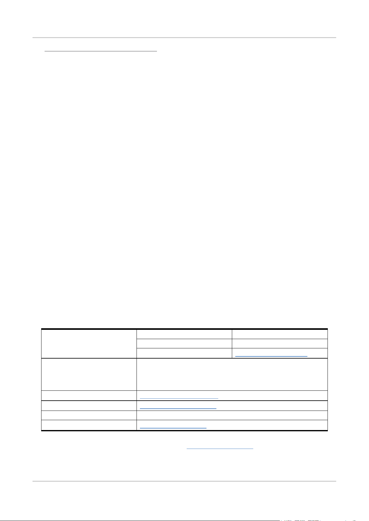
1.1. FX Series Product Comparison
The following table lists the main feature differences between the two FX series variants.
Table 1. FXT009 and FX100 Feature Comparison
4112221 Rev 7.2 June 19, 2013 15
Page 16
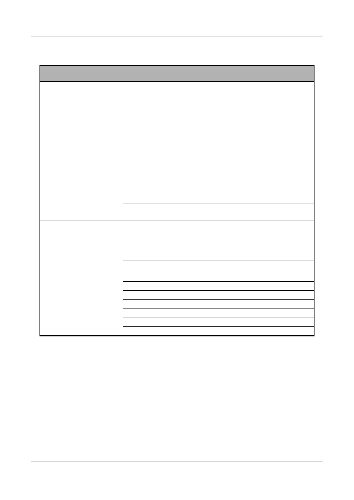
Overview
Feature
FXT009
FX100
gpsOneXTRATM
- Embedded GPS
-
Primary RF Interface
Secondary RF Interface
- GPS MMCX Connector Interface
-
USB Interface
10-pin Micro-Fit Connector Interface
15-pin sub-D Serial Interface
Length
89 mm
Width
60 mm
Thickness
30 mm
Weight
100g for FXT009
125g for FX100
User Guide
For more information on the features available on the FX Series variants, refer to Table 4 FX Series
Basic Features.
1.2. Overall Dimensions
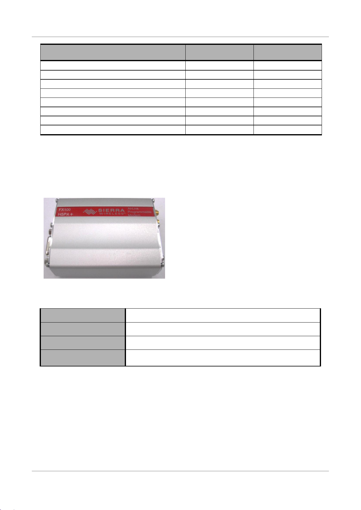
Figure 1. FX Series Modem
Table 2. FX Series Physical Dimensions
4112221 Rev 7.2 June 19, 2013 16
Page 17

Overview
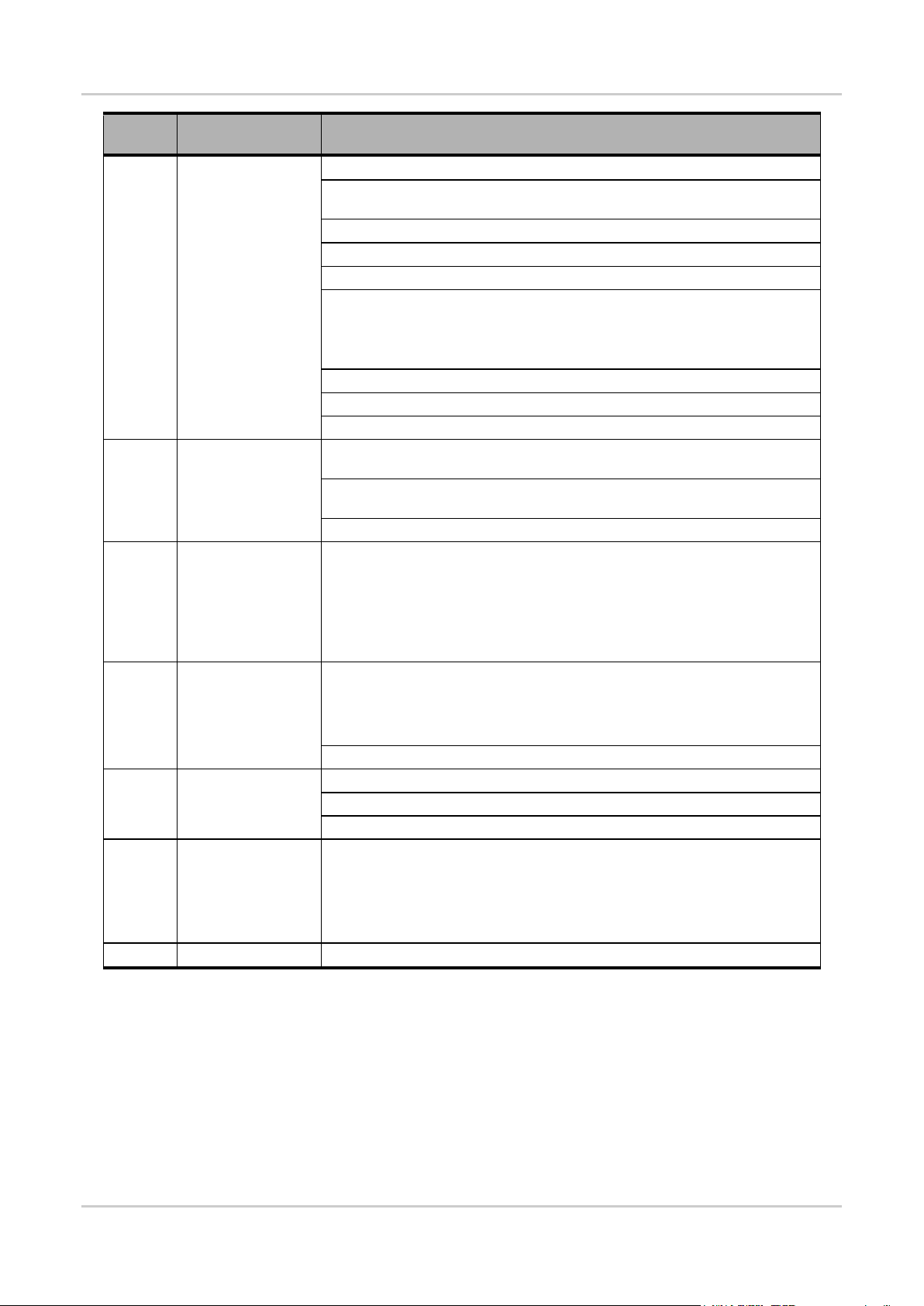
Product
Bundle
Description
FXT009
Standard
Wireless connectivity: EGSM Quad Band + CL 10 GPRS + EDGE
Wired connectivity: Serial, USB
Accessories: DC Cable, USB cable, Holding Bridles
Ready to Use
Wireless connectivity: EGSM Quad Band + CL 10 GPRS + EDGE
Wired connectivity: Serial, USB
Accessories: DC Cable, USB cable, Holding Bridles, Cellular Antenna, Power
Supply, Data Cable
Ready to Use
Ethernet
Wireless connectivity: EGSM Quad Band + CL 10 GPRS + EDGE
Wired connectivity: Serial, USB, Ethernet
Accessories: DC Cable, USB cable, Holding Bridles, Cellular Antenna, Power
Supply, Data Cable, FXTE02 Ethernet X-card, Ethernet RJ45 dongle
FX100
Standard
Wireless connectivity: EGSM Quad Band + CL 12 GPRS + EDGE + HSxPA +
Penta Band HSPA+
Wired connectivity: Serial, USB
Accessories: DC Cable, Holding Bridles
Ready to Use
Wireless connectivity: EGSM Quad Band + CL 12 GPRS + EDGE + HSxPA +
Penta Band HSPA+
Wired connectivity: Serial, USB
Accessories: DC Cable, USB cable, Holding Bridles, Cellular Antenna,
Diversity Antenna, GPS Antenna, Power Supply, Data Cable
User Guide
1.3. FX Series Variants and Bundles
Table 3. FX Series Variants
Note: Available wireless interfaces will vary depending on the FX Series variant. Refer to Table 4 FX
Series Basic Features for more details on the basic features available on each variant.
1.4. Connections
10-pin Micro-Fit Power Supply Connector
USB Interface
15-pin Sub-D Serial Interface
SIM Interface
Antenna Interface
SMA Main
SMA Diversity (3G-HSxPA version) for FX100
GPS for FX100
1.5. Interfaces
1.5.1. External Interfaces
Power Supply
3V/1V8 SIM Interface
USB (slave) Interface
Serial Link (UART1)
4112221 Rev 7.2 June 19, 2013 17
Page 18

Overview
This electronic product is subject to the EU Directive 2002/96/EC for Waste Electrical
and Electronic Equipment (WEEE). As such, this product must not be disposed of at a
municipal waste collection point. Please refer to local regulations for directions on
how to dispose of this product in an environmental friendly manner.
User Guide
ON/OFF
Boot (for FXT009 only)
Reset
Audio Interface
2 GPIOs
LED Status Indicator
1.5.2. Internal X-card Interface
1 – Secondary Serial Link (UART2)
6 – GPIOs
2 – SPI Bus
1 – ADC
1 – DAC (except for FX100)
1 – PCM
1 – Interrupt
Reset access to the embedded module
Boot access to the embedded module (except for FX100)
2.8V supply from the FX Series
4V supply from the FX Series
2.8V Digital supply from the embedded module
1.8V Digital supply from the embedded module
Access to 4.75 to 32V DC-IN
1.6. Environmental Compliance
1.6.1. RoHS Directive Compliant
The FX Series is compliant with RoHS Directive 2011/65/EC which sets limits for the use of certain
restricted hazardous substances. This directive states that “from 1st July 2006, new electrical and
electronic equipment put on the market does not contain lead, mercury, cadmium, hexavalent
chromium, polybrominated biphenyls (PBB) or polybrominated diphenyl ethers (PBDE)”.
1.6.2. Disposing of the Product
4112221 Rev 7.2 June 19, 2013 18
Page 19
2. Features and Services
Features
Description
Open AT
Application
Framework
Open AT Application Framework programmable:
Native execution of embedded standard ANSI C applications
Custom AT command creation
Custom application library creation
Standalone operation
Interface for embedded applications
Library compatible
Standard
850MHz / 900 MHz
E-GSM compliant
Output power: class 4 (2W)
Fully compliant with ETSI GSM
phase 2 + normal MS
1800 MHz / 1900MHz
Output power: class 1 (1W)
Fully compliant with ETSI GSM
phase 2 + normal MS
GPRS
Class 10
Class 12 (FX100 only)
PBCCH support
Coding schemes: CS1 to CS4
Compliant with SMG31bis
Embedded TCP/IP stack
EGPRS
Class 10
Class 12 (FX100 only)
PBCCH support
Coding schemes: MCS1 to MCS9
Compliant with SMG31bis
Embedded TCP/IP stack
Interface
RS232 (V.24/V.28) Serial interface supporting:
Baud rate (bits/s): 300, 600, 1200, 2400, 4800, 9600, 19200, 38400, 57600,
115200, 230400, 460800 and 921600
Autobauding (bits/s): from 1200 to 921600
2 General Purpose Input/Output gates (GPIOs) available
1.8 V / 3 V SIM interface
AT command set based on V.25ter and GSM 07.05 & 07.07
SMS
Text & PDU
POINT TO POINT (MT/MO)
Cell broadcast
This section enumerates the features and services available on the FX Series.
2.1. Features and Services
Refer to the table below for the list of basic features available on the FX Series.
Table 4. FX Series Basic Features
4112221 Rev 7.2 June 19, 2013 19
Page 20
Features and Services
Features
Description
Data
Data circuit asynchronous
Transparent and Non Transparent modes
Up to 14.400 bits/s
MNP Class 2 error correction
V42.bis data compression
UMTS Data
Transfer
(FX100 only)
BAND I, II, V, VI, VIII (2100/1900/850/800/900) up to 384kbits/s
HSXPA
(FX100 only)
BAND I, II, V, VI, VIII (2100/1900/850/800/900)
HSDPA Cat 10 up to 14.4Mbits/s
HSUPA Cat 6 up to 5.76Mbits/s
FAX
(FXT009 only)
Automatic fax group 3 (class 1 and class 2)
Audio
Echo cancellation
Noise reduction
Full Rate, Enhanced Full Rate, Half Rate operation and Adaptive Multi-Rate
(FR/EFR/HR/AMR)
Dual Tone Multi Frequency function (DTMF). Note that this can be supported by
FX100 with Firmware 7.52.A1 or later.
User Guide
2.2. Supported Bands
The FX Series come in two variants, supporting various bearers and bands. The FXT009 is a quad
band programmable modem that support either EU bands (EGSM900/DCS1800) or US bands
(GSM850/PCS1900). Users may switch from one supported band to another by using AT commands.
The FX100 is also a quad band EGSM900/DCS1800/GSM850/PCS1900 that also supports penta
band UMTS/HSPA (WCDMA-FDD) 2100/1900/850/800/900 (Band I, II, V, VI and VIII). Band selection
is done automatically without having to switch manually using AT commands.
Refer to sections 9.4 Checking the Band Selection and 9.5 Switching Bands for more information
regarding switching bands.
2.3. X-card Interface
The FX Series offers a 50-pin X-card interface accessible to customers. It is an additional interface for
customers to expand their application features by simply plugging in an X-card through the mating
connector of the X-card interface.
Refer to section 7 X-card for more information about the X-card supported by the FX Series.
4112221 Rev 7.2 June 19, 2013 20
Page 21

Features and Services
User Guide
2.4. Protection
2.4.1. Power Supply
The FX Series is protected from continuous over-voltage by a 2A/250V slow break fuse directly
bonded on the 6-wire cable accessory; and it is also protected against transient voltage peaks over
+32V. When the input voltage exceeds 32V, the supply voltage is automatically disconnected in order
to protect the internal electronic components from overvoltage.
2.4.2. Electrostatic Discharge
The FX Series withstands ESD according to IEC 1000-4-2 requirements for all accessible parts,
except for the RF connector which withstands ESD as follows:
+/- 8kV of air discharge
+/- 4kV of contact discharge
2.4.3. Main Serial Link
The FX Series’ RS232 serial link connection is internally protected against electrostatic surges on its
lines by ESD protection and it also has the following filtering guarantees:
EMI/RFI protection on both input and output
Signal smoothing
4112221 Rev 7.2 June 19, 2013 21
Page 22
3. Functional Specifications
This section discusses the functional specifications of the FX Series.
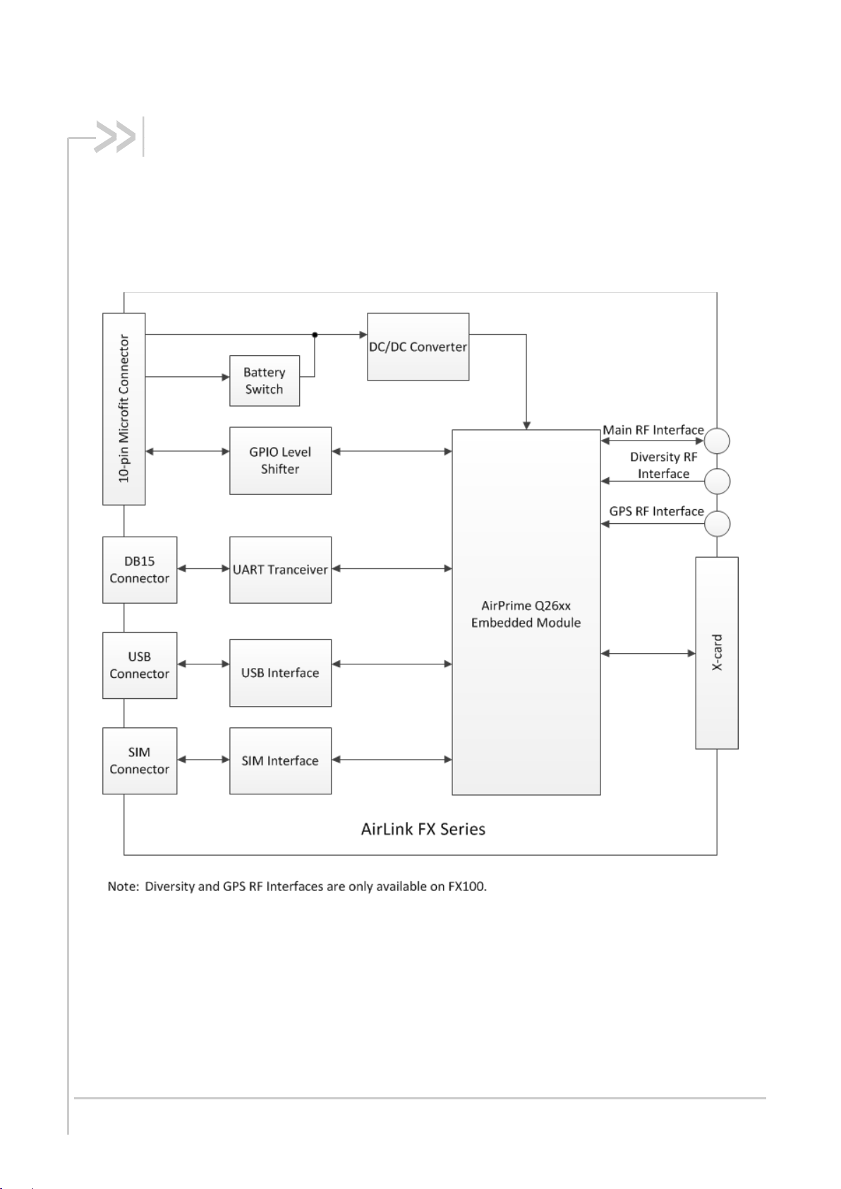
3.1. Functional Architecture
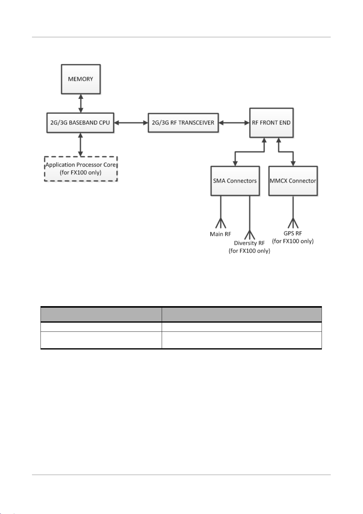
The global architecture of the FX Series is shown in the figure below.
Figure 2. Functional Architecture
4112221 Rev 7.2 June 19, 2013 22
Page 23
Functional Specifications
FX Series Variant
Supported Bands
FXT009
Quad band (850/900/1800/1900 MHz)
FX100
Quad band (850/900/1800/1900 MHz)
Penta band UMTS/HSXPA (800/850/900/1900/2100 MHz)
User Guide
3.2. RF Functionalities
Figure 3. FX Series RF Architecture
Refer to the table below for the list of FX Series variants and their corresponding supported bands.
Table 5. FX Series Variants with Corresponding Supported Bands
3.3. Operating System
The FX Series is Open AT Application Framework compliant. With the Open AT Application
Framework, customers can embed their own applications with the FX Series and turn the FX Series
into a solution for their specific market need. The operating system of the FX Series is also
responsible for the following functions:
AT Command processing
Real Time Clock (RTC) with calendar
4112221 Rev 7.2 June 19, 2013 23
Page 24
4. Technical Specifications
Operating Voltage Range
4.75V to 32V DC, nominal at 13.2V
Maximum Current (Typical)
600mA, average at 4.75V; 3A Peak at 4.75V on FXT009
850mA, average at 4.75V; 3.7A Peak at 4.75V on FX100
4.1. Power Supply
The FX Series is supplied by an external DC voltage, DC-IN, with a voltage range of +4.75V to +32V.
The main regulation is made with an internal DC/DC converter in order to supply all the internal
functions with a DC voltage. The correct operation of the FX Series in Communication mode is not
guaranteed if the input voltage falls below 4.75V.
Refer to the following table for the FX Series’ operating voltage range and maximum current.
Table 6. Power Supply Electrical Characteristics
The FX Series is permanently powered once the power supply is connected. In the case of Alarm
mode (Low Power mode), the user can set the FX Series “Turn-on” time. Refer to section 6.1 Alarm
Mode for more information.
Caution: The minimum input voltage specified here is the FX Series input. Be mindful of the input voltage
decrease caused by the power cable. When using the 6-wire cable accessory that comes with the
FX Series package, this input drop is at around 800mV at 4.75V and 220mV at 32V (EDGE 4TX).
The FX Series is designed for use with the original power cable, and the fuse that came with the
original cable is a 2A/250V Slow Break fuse 5.2mm*20mm.
4112221 Rev 7.2 June 19, 2013 24
Page 25
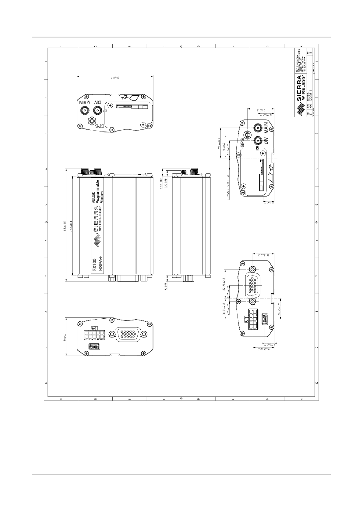
Technical Specifications
User Guide
4.2. Mechanical Specifications
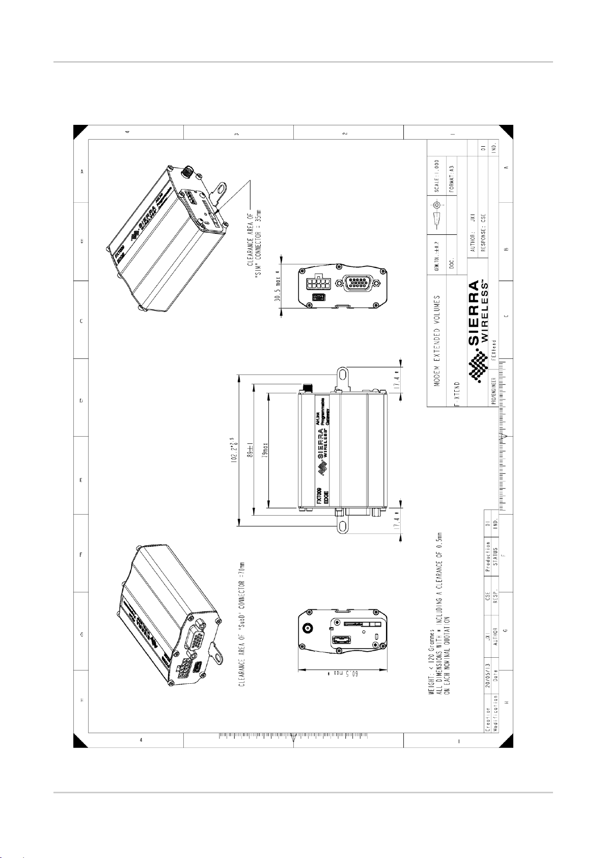
Figure 4. FXT009 Mechanical Drawing
4112221 Rev 7.2 June 19, 2013 25
Page 26
Technical Specifications
User Guide
Figure 5. FX100 Mechanical Drawing (1 of 2)
4112221 Rev 7.2 June 19, 2013 26
Page 27
Technical Specifications
User Guide
Figure 6. FX100 Mechanical Drawing (2 of 2)
4112221 Rev 7.2 June 19, 2013 27
Page 28
5. Interfaces
Mini-B USB Interface
15-pin Sub-D Serial Interface
10-pin Micro-Fit Connector
This section describes the different interfaces that connect with the FX Series. The FX Series comes
with the following interfaces:
10-pin Micro-Fit Connector
USB Interface (mini-B connector)
15-pin Sub-D Serial Interface
Main RF Interface
Secondary RF Interface (for FX100 only)
GPS RF Interface (for FX100 only)
SIM Interface
LED Status Indicator
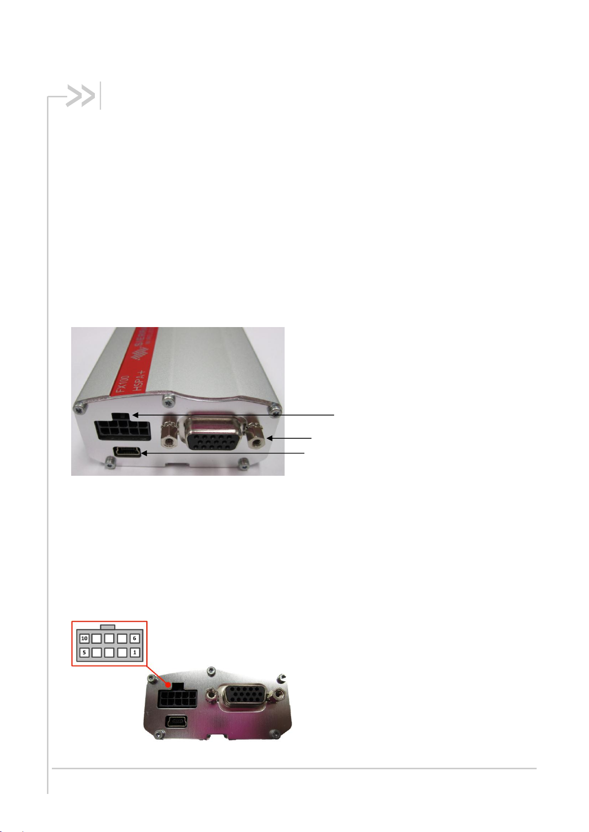
5.1. Front Interface
Figure 7. FX Series Front Interface
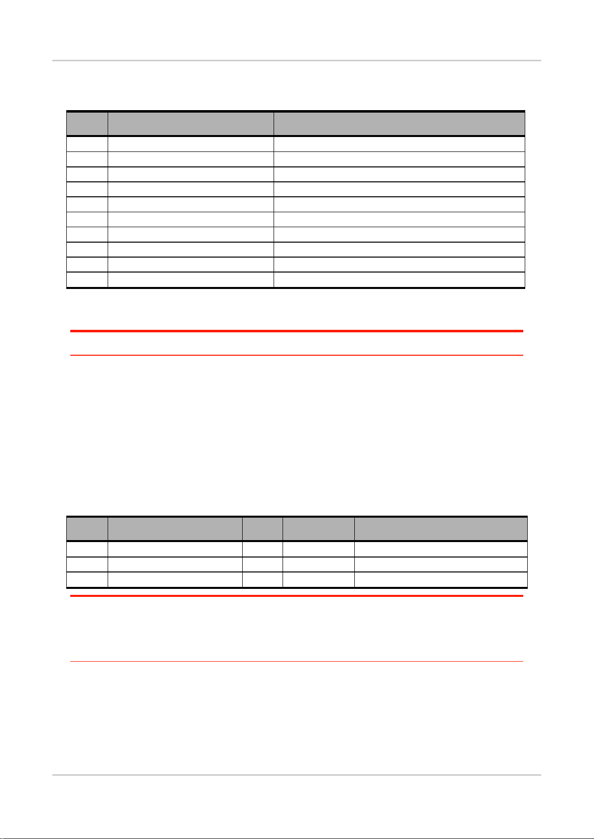
5.1.1. Power Supply Connector
The power supply connector is a 10-pin Micro-Fit connector that is used for:
External DC Power Supply connection with voltage from +4.75V to +32V, at 3A on FXT009
and 3.7A on FX100
GPIOs connection and GPIO voltage reference
ON/OFF pin to power OFF the FX Series
Figure 8. Power Supply Connector
4112221 Rev 7.2 June 19, 2013 28
Page 29
Interfaces
Pin #
Signal
Description
1
GPIO25 (GPIO35 for FX100)
General purpose input/output
2
GPIO21
General purpose input/output
3
Vref
Voltage reference for the GPIOs
4
Reserved
Reserved
5
Reserved
Reserved
6
GND
Ground
7
DC-IN
Input Supply for the FX Series (4.75V to 32V)
8
ON/OFF
Control pin to power OFF the FX Series
9
Reserved
Reserved
10
Reserved
Reserved
Pin #
Signal
I/O
I/O Voltage
Description
1
GPIO21
I/O
Vref
General purpose input/output
2
GPIO25 (GPIO35 for FX100)
I/O
Vref
General purpose input/output
3
Vref I 2.8V ~ 15V
Voltage reference for the GPIOs
User Guide
Refer to the following table for the pin description of the power supply connector.
Table 7. Power Supply Connector Pin Description
The input voltage range (DC-IN) is from 4.75V to 32V, with a typical operating voltage of 13.2V.
The power cable is provided as part of the FX Series package.
Caution: Pins 1, 2, 3, 4, 5, 8, 9 and 10 are low voltage interfaces. It is strictly prohibited to connect these pins
to any power supply as there is a risk of damaging the FX Series.
5.1.1.1. General Purpose Input/Output
The FX Series has two external GPIO ports, GPIO21 and GPIO25 (GPIO35 for FX100); as well as a
voltage reference line, Vref.
Vref sets the reference voltage of the input or output of the two GPIOs. Leaving it unconnected sets
the GPIO level at 2.3V – 2.6V by default. It is strongly recommended to connect to the required
GPIOs’ output voltage (2.8V ~ 15V).
Refer to the following table for the pin description of the GPIOs.
Table 8. GPIO Pin Description
Note: It is recommended to use a 6-wire cable accessory for easy access to these three lines. Please
refer to section 13.1 Standard Accessories for more information about the 6-wire cable accessory.
When the voltage reference, Vref, is not connected, if one of the GPIO output is in High state while
the other is in Low state, the GPIO in high level voltage will be at 2.3V.To avoid this voltage drop, it
is recommended to use Vref to the desired output voltage.
4112221 Rev 7.2 June 19, 2013 29
Page 30
Interfaces
Parameter
Mininum
Typical
Maximum
Condition
VIL
0.84V
Please refer to Figure 9.
VIH
1.96V
Please refer to Figure 10.
VOL
0.4*
Please refer to Figure 11.
VOH
2.8*
FX Series Zout = 100K Pull-up to Vref, please
refer to Figure 12.
User Guide
With Vref connected to 2.8V, both GPIO21 and GPIO25 (GPIO35 for FX100) may be interfaced with a
component that complies with the following levels.
Table 9. GPIO Pin Operating Conditions when Vref is at 2.8V
* Value without external load.
Figure 9. Equivalent Circuit of VIL, Vref = 2.8V
Figure 10. Equivalent Circuit of VIH, Vref = 2.8V
Figure 11. Equivalent Circuit of VOL, Vref = 2.8V
4112221 Rev 7.2 June 19, 2013 30
Page 31

Interfaces
Parameter
Min
Typ
Max
Condition
VIL
0.84V
Please refer to Figure 13.
VIH
1.96V
Please refer to Figure 14.
VOL
*
058.0
110
Vref
Please refer to Figure 15.
VOH
Vref*
FX Series Zout = 100K Pull-up to Vref, please
refer to Figure 16.
User Guide
Figure 12. Equivalent Circuit of VOH, Vref = 2.8V
With Vref > 2.8V, both GPIO21 and GPIO25 (GPIO35 for FX100) may be interfaced with a
component that complies with the following levels.
Table 10. GPIO Pin Operating Conditions when Vref > 2.8V
* Value without external load.
Figure 13. Equivalent Circuit of VIL, Vref > 2.8V
Figure 14. Equivalent circuit of VIH, Vref > 2.8V
4112221 Rev 7.2 June 19, 2013 31
Page 32

Interfaces
User Guide
Figure 15. Equivalent circuit of VOL, Vref > 2.8V
Figure 16. Equivalent circuit of VOH, Vref > 2.8V
The GPIO pin is mainly used to:
Act as a switch for a transistor when the GPIO is configured as output.
Act as a status reading when the GPIO is configured as input.
The GPIOs may be controlled with the following AT commands:
AT+WIOW for write access to the GPIO value, when the GPIO is used as an output
AT+WIOR for read access to the GPIO value, when the GPIO is used as an input
By default, and when the FX Series has been reset, both GPIOs are configured as inputs. The AT
command AT+WIOM must be used to change this configuration. Refer to documents [1] Open AT
Application Framework AT Commands Interface Guide and [2] AirPrime SL808xT and Q2698 Open
AT Framework Commands Interface Guide for more information regarding this AT command.
5.1.1.1.1. Setting the GPIO as an Output
Refer to the following example for how to configure the GPIO as an output.
Enter the following commands:
AT+WIOM=1,“GPIO21”,1,0 this command activates GPIO21 as an
output and sets it at a low level.
AT+WIOW=“GPIO21”,1 this command sets the output level of
GPIO21 to HIGH.
4112221 Rev 7.2 June 19, 2013 32
Page 33

Interfaces
Condition
State
Power Supply
Operation
1
Open
When 4.75V to 32V supply is
applied.
The FX Series is turned ON.
2
Pulled to GND
When 4.75V to 32V supply is
applied.
The FX Series remains OFF.
3
Left open when turning
ON the FX Series,
then pulled to GND
4.75V to 32V supply is initially
applied.
The FX Series remains ON and will
remain ON until AT+CPOF is sent to
turn the device OFF.
Pin #
Signal
I/O
I/O Voltage
Description
8
ON/OFF
I
4V
Pin to turn the FX Series ON/OFF.
User Guide
5.1.1.1.2. Setting the GPIO as an Input
Refer to the following example for how to configure the GPIO as an input.
Enter the following commands:
AT+WIOM=1,“GPIO21”,0 this command activates GPIO21 as an input.
AT+WIOR=“GPIO21” this command reads the GPIO21 level and
returns the value “1” which represents a HIGH level.
Pull the GPIO21 pin to GND, and read again. The return value should now be “0” which
represents a LOW level.
Refer to documents [1] Open AT Application Framework AT Commands Interface Guide and [2]
AirPrime SL808xT and Q2698 Open AT Framework Commands Interface Guide for more information
regarding AT commands.
Note: The AT+WIOW and AT+WIOR commands will automatically set the GPIO to the desired mode. For
example, AT+WIOW=42,1 will set GPIO42 to output mode and in High state.
5.1.1.2. ON/OFF Pin
The FX Series has an external ON/OFF pin which is used to turn the device ON or OFF. The following
table describes the operation of this pin.
Table 11. ON/OFF Pin Operation
To enable the low power mode, the user may simply pull the ON/OFF pin to GND and send
AT+CPOF to the FX Series using a communication software such as a HyperTerminal.
Table 12. ON/OFF Pin Description
Refer to the power consumption tables in section 11 Power Consumption for the power consumption
values when the FX Series is in Alarm mode (Low Power mode).
4112221 Rev 7.2 June 19, 2013 33
Page 34

Interfaces
Pin #
Signal
I/O
I/O Type
Reset State
Description
1
CT109/DCD
O
+/- 5.5V
Undefined
Data Carrier Detect
2
CT103/TXD
I
+/- 5.5V
Z
Transmit Serial Data
3
BOOT*
I
1V8
BOOT. This signal must not be
connected. Its use is strictly reserved
for Sierra Wireless or competent
retailers.
4
CMIC2P
I
Analog
Microphone positive input
5
CMIC2N
I
Analog
Microphone negative input
6
CT104/RXD
O
+/- 5.5V
1
Receive Serial Data
7
CT107/DSR
O
+/- 5.5V
Z
Data Set Ready
8
CT108-2/DTR
I
+/- 5.5V
Z
Data Terminal Ready
9
GND
GND
Ground
10
CSPK2P
O
Analog
Speaker positive input
11
CT106/CTS
O
+/- 5.5V
Z
Clear To Send
12
CT105/RTS
I
+/- 5.5V
Z
Request To Send
13
CT125/RI
O
+/- 5.5V
Undefined
Ring Indicator
14
RESET
I/O
1V8 FX Series Reset
15
CSPK2N
O
Analog
Speaker negative input
User Guide
5.1.2. Serial Interface
A SUB-D 15-pin connector is available as a serial interface to directly communicate with the FX Series.
This serial interface is used for:
RS232 serial link connection
Audio lines connection (microphone and speaker)
BOOT signal connection (not used in FX100)
RESET signal connection
Figure 17. 15-Pin Serial Connector
Refer to the following table for the pin description of the 15-pin serial connector.
Table 13. Serial Connector Pin Description
* Not used in FX100.
4112221 Rev 7.2 June 19, 2013 34
Page 35

Interfaces
User Guide
5.1.2.1. RS232 Serial Link Connection
Also known as the main serial link, the RS232 interface performs the voltage level adaptation
(V24/CMOS ⇔ V24/V28) between the internal FX Series (DCE) and external applications (DTE).
The signals available on the RS232 serial link are as follows:
TX data (CT103/TXD)
RX data (CT104/RXD)
Request To Send (CT105/RTS)
Clear To Send (CT106/CTS)
Data Terminal Ready (CT108-2/DTR)
Data Set Ready (CT107/DSR)
Data Carrier Detect (CT109/DCD)
Ring Indicator (CT125/RI)
Figure 18. RS232 Serial Link Signals
The RS232 interface has been designed to allow flexibility in the use of the serial interface signals.
However, the use of TXD, RXD, CTS and RTS signals are mandatory; while the use of DTR, DSR,
DCD and RI signals are optional.
Tip: The FX Series is designed to operate using all serial interface signals and it is recommended to use
CT105/RTS and CT106/CTS for hardware flow control in order to avoid data corruption during
transmission.
The FX Series also implements the Serial Port Auto Shut Down feature with the DTR signal. It is
recommended to use the CT108-2/DTR signal to benefit from the current consumption
improvement performed by this feature.
5.1.2.2. RS232 Implementation
The following subsections describe how the RS232 serial link can be implemented to suit different
designs.
5.1.2.2.1. 5-wire Serial Interface RS232 Implementation
The signals used in this interface are as follows:
CT103/TXD
CT104/RXD
4112221 Rev 7.2 June 19, 2013 35
Page 36

Interfaces
User Guide
CT105/RTS
CT106/CTS
CT108-2/DTR
Note: The CT108-2/DTR signal must be managed following the V24 protocol signaling if the Sleep Idle
Mode and Serial Port Auto Shut Down feature are to be used.
Figure 19. V24 Serial Link Implementation for a 5-wire UART
5.1.2.2.2. 4-wire Serial Interface RS232 Implementation
The signals used in this interface are as follows:
CT103/TXD
CT104/RXD
CT105/RTS
CT106/CTS
Figure 20. V24 Serial Link Implementation for a 4-wire UART
5.1.2.2.3. 2-wire Serial Interface RS232 Implementation
The signals used in this interface are as follows:
CT103/TXD
CT104/RXD
Note: Although this case is possible, it is not recommended.
The flow control mechanism must be managed from the customer end.
4112221 Rev 7.2 June 19, 2013 36
Page 37

Interfaces
User Guide
Figure 21. V24 Serial Link Implementation for a 2-wire UART
The CT105/RTS and the CT106/CTS signals are not used in this configuration. Configure the AT
command AT+IFC=0,0 to disable the flow control function. Refer to documents [1] Open AT
Application Framework AT Commands Interface Guide and [2] AirPrime SL808xT and Q2698 Open
AT Framework Commands Interface Guide for more information regarding AT Commands.
For more information on how to use the RS232 serial link to communicate with the FX Series, refer to
section 5.1.2.1 RS232 Serial Link Connection.
5.1.2.3. Autobauding Mode
The autobauding mode allows the FX Series to detect the baud rate used by the DTE connected to
the RS232 serial link. The autobauding mode is controlled by AT commands. Refer to documents [1]
Open AT Application Framework AT Commands Interface Guide and [2] AirPrime SL808xT and
Q2698 Open AT Framework Commands Interface Guide for more information.
5.1.2.4. Serial Port Auto Shut Down Feature
The RS232 serial link can be shut down when there is no activity between the DTE and the FX Series.
This can help improve the power consumption performance.
The Serial Port Auto Shut Down feature is controlled by the AT command AT+WASR. Enter:
AT+WASR=1 to enter the serial port auto shut down mode
AT+WASR=0 to exit the serial port auto shut down mode
Refer to documents [1] Open AT Application Framework AT Commands Interface Guide and [2]
AirPrime SL808xT and Q2698 Open AT Framework Commands Interface Guide for more information
on AT commands.
Caution: GPIO24 is reserved for serial port auto shut down feature. It is prohibited for customer use.
Improper access to GPIO24 by customers may lead to unexpected behavior on serial port
performance.
It is prohibited to use the serial port auto shut down feature when the CT108-2/DTR is not used in
the application. Otherwise, there will be data lost from the DTE side to the FX Series.
4112221 Rev 7.2 June 19, 2013 37
Page 38

Interfaces
(Sub D
15-pin)
Pin #
Signal
I/O
I/O Type
Description
4
CMIC2P
I
Analog
Microphone positive input
5
CMIC2N
I
Analog
Microphone negative input
(Sub D
15-pin)
Pin #
Signal
I/O
I/O Type
Description
4
CMIC1P
I
Analog
Microphone positive input
5
CMIC1N
I
Analog
Microphone negative input
DC Equivalent Circuit
AC Equivalent Circuit
User Guide
5.1.2.5. Audio Lines Connection
The FX Series supports one microphone input and one speaker output.
5.1.2.5.1. Microphone
The microphone inputs are connected in differential mode to reject common mode noise and TDMA
noise. The microphone inputs have already included biasing for an electrets microphone (0.5mA and
2V) and are ESD protected. An electret microphone may be directly connected to these inputs
allowing an easy connection to a headset.
The microphone gain can be adjusted by AT+VGT and the transmit digital gain can be adjusted by
AT+WDGT. Refer to documents [1] Open AT Application Framework AT Commands Interface Guide
and [2] AirPrime SL808xT and Q2698 Open AT Framework Commands Interface Guide for more
information about these AT commands.
The following table shows the pin assignments of the microphone input. Note that there is a difference
in the microphone signal names used between FXT009 and FX100.
Table 14. Microphone Pin Description for FXT009
Table 15. Microphone Pin Description for FX100
Table 16. Equivalent Circuits of CMIC
4112221 Rev 7.2 June 19, 2013 38
Page 39

Interfaces
Parameters
Min
Typ
Max
Unit
Internal biasing
DC Characteristics
MIC 2 2.1
2.2
V
Output current
0.5
1.5
mA
R
1650
1900
2150
AC Characteristics
200 Hz<F<4 kHz
Z CMICxP
(CMICxN=Open)
1.1
1.3
1.6
k
Z CMICxN
(CMICxP=Open)
Z CMICxP
(CMICxN=GND)
0.9
1.1
1.4
Z CMICxN
(CMICxP=GND)
Impedance between
CMICxP and CMICxN
1.3
1.6
2
Working voltage
(CMICxP-CMICxN)
AT+VGT*=3500dB
13.8
mVrms
AT+VGT*=2000dB
77.5
AT+VGT*=700dB
346
Maximum rating voltage
(CMICxP or CMICxN)
Positive
+7.35**
V
Negative
-0.9
Parameters
Min
Typ
Max
Unit
DC Characteristics
N/A V
AC Characteristics 200 Hz<F<4
kHz
Z
70
120
160
k
Working voltage
(CMICxP-CMICxN)
AT+VGT*=3500dB
13.8
mVrms
AT+VGT*=2000dB
77.5
AT+VGT*=700dB
346
Maximum rating voltage
(CMICxP or CMICxN)
Positive
+7.35**
V
Negative
-0.9
User Guide
Table 17. Electrical Characteristics of CMIC for FXT009
* The input voltage depends of the input micro gain set by AT command. Refer to document [1] Open AT
Application Framework AT Commands Interface Guide.
** Because CMICxP is internally biased, it is necessary to use a coupling capacitor to connect an audio signal
provided by an active generator. Only a passive microphone can be directly connected to the CMICxP and CMICxN inputs.
Table 18. Electrical Characteristics of CMIC for FX100
* The input voltage depends of the input micro gain set by AT command. Refer to document [2] AirPrime
SL808xT and Q2698 Open AT Framework Commands Interface Guide.
** Because CMICxP is internally biased, it is necessary to use a coupling capacitor to connect an audio signal
provided by an active generator. Only a passive microphone can be directly connected to the CMICxP and CMICxN inputs.
4112221 Rev 7.2 June 19, 2013 39
Page 40

Interfaces
Feature
Values
Type
Electret 2V/0.5 mA
Impedance
Z = 2k
Sensitivity
-40dB to -50dB
SNR
> 50dB
Frequency response
Compatible with GSM specifications
(Sub D
15-pin)
Pin #
Signal
I/O
I/O Type
Description
10
CSPK2P
O
Analog
Speaker positive output
15
CSPK2N
O
Analog
Speaker negative output
(Sub D
15-pin)
Pin #
Signal
I/O
I/O Type
Description
10
CSPK1P
O
Analog
Speaker positive output
15
CSPK1N
O
Analog
Speaker negative output
User Guide
Refer to the following table for the list of recommended microphone characteristics.
Table 19. Recommended Microphone Characteristics
5.1.2.5.2. Speaker
The speaker outputs are connected in differential mode to reject common mode noise and TDMA
noise.
Speaker outputs are connected to internal push-pull amplifiers and may be loaded down with
components between 32 – 150Ω and up to 1nF. These outputs may be directly connected to a
speaker.
The output power may be adjusted by 2dB steps. The gain of the speaker outputs is internally
adjusted and may be tuned using the AT+VGR command. Furthermore, the digital gain can be
adjusted using AT+WDGR. Refer to documents [1] Open AT Application Framework AT Commands
Interface Guide and [2] AirPrime SL808xT and Q2698 Open AT Framework Commands Interface
Guide for more information about these AT commands.
The following table shows the pin assignments of the speaker output. Note that there is a difference in
the speaker signal name used between FXT009 and FX100.
Table 20. Speaker Outputs Pin Description for FXT009
Table 21. Speaker Outputs Pin Description for FX100
Figure 22. Equivalent Circuit of CSPK
4112221 Rev 7.2 June 19, 2013 40
Page 41

Interfaces
Parameters
Min
Typ
Max
Unit
Biasing voltage
CSPKxP and CSPKxN
1.30
V
Output swing
voltage
RL=8: AT+VGR=-1000*; differential
- - 4
Vpp
RL=32: AT+VGR=-1000*; differential
- - 5
Vpp
RL
Load resistance
6 8 -
IOUT
Output current; peak value; RL=8
- - 180
mA
POUT
RL=8; AT+VGR=-1000*;
- - 250
mW
RPD
Output pull-down resistance at power-down
28
40
52
k
VPD
Output DC voltage at power-down
- - 100
mV
Parameters
Min
Typ
Max
Unit
Biasing voltage
CSPKxP and CSPKxN
-1.5 1.5
mV
Output swing
voltage
RL=16Ω: AT+VGR=-1600*; single-ended
-
1.7 Vpp
RL=32Ω: AT+VGR=-1600*; single-ended
-
1.9
2.75
Vpp
RL
Load resistance
14.5
32 - Ω
IOUT
Output current; peak value; RL=16Ω
-
40
85
mA
Output current; peak value; RL=32Ω
-
22 - mA
POUT
RL=16Ω; AT+VGR=-1600*
-
25 - mW
RL=32Ω; AT+VGR=-1600*
-
16
27
mW
RPD
Output pull-down resistance at power-down
28
40
52
kΩ
Feature
Values
Type
10mW, electro-magnetic
Impedance
Z = 30 to 50
Sensitivity
110dB SPL min. (0dB = 20µPa)
Frequency response
Compatible with GSM specifications
User Guide
Table 22. Electrical Characteristics of CSPK for FXT009
* The output voltage depends of the output speaker gain set by AT command. Refer to document [1] Open AT
Application Framework AT Commands Interface Guide. This value is given in dB, but it’s possible to toggle this to index
value.
Table 23. Electrical Characteristics of CSPK for FX100
* The output voltage depends of the output speaker gain set by AT command. Refer to document [2] AirPrime
SL808xT and Q2698 Open AT Framework Commands Interface Guide. This value is given in dB, but it’s possible to toggle
this to index value.
Refer to the following table for the list of recommended speaker characteristics.
Table 24. Recommended Speaker Characteristics
4112221 Rev 7.2 June 19, 2013 41
Page 42

Interfaces
Pin #
Signal
Description
1
VBUS
+5V Power supply
2
D-
Differential data interface positive
3
D+
Differential data interface negative
4
ID
Not connected
5
GND
Ground
Parameter
I/O
Min
Typ
Max
Unit
VBUS
I
4.75
5 V
D-, D+
I/O 3 3.3
3.6
V
VBUS Input current consumption
100
mA
Parameter
I/O
Min
Typ
Max
Unit
VBUS
Input
4.75
5 V
D-, D+ (Low / Full speed)
Input High
2.00
3.30
3.60
V
Input Low
0 0.80
V
Output High
2.80
3.30
3.60
V
Output Low
0.30
V
User Guide
5.1.3. USB Interface
Aside from the serial interface, the Mini-B USB interface (USB slave) may also be used to directly
communicate with the FX Series.
Figure 23. Mini-B USB Connector
Refer to the following table for the pin description of the mini-B USB connector.
Table 25. Mini-B USB Pin Description
The FXT009 USB slave interface complies with USB 2.0 protocol signaling but not with USB 2.0
electrical interface; while the FX100 can support both USB 2.0 protocol signaling and electrical
interface.
The USB interface features:
12Mbit/s full speed transfer rate for FXT009; 480Mbit/s high-speed transfer rate for FX100
3.3V type compatible
USB Soft-connect feature
USB Download feature (only supported by FX100)
CDC 1.1 – ACM compliant
Table 26. USB Electrical Characteristics for FXT009
Table 27. USB Electrical Characteristics for FX100
4112221 Rev 7.2 June 19, 2013 42
Page 43

Interfaces
Parameter
I/O
Min
Typ
Max
Unit
D-, D+ (High speed)
Input High
0.30
0.44
V
Input Low
0 0.01
V
Output High
0.36
0.38
0.44
V
Output Low
0 0.01
V
SIM Interface
Main RF Interface
X-card Compartment
User Guide
The USB feature can be activated by using the AT+WMFM=0,1,3 AT command. Refer to documents
[1] Open AT Application Framework AT Commands Interface Guide and [2] AirPrime SL808xT and
Q2698 Open AT Framework Commands Interface Guide for more information regarding this AT
command.
5.2. Back Interface
LED Status Indicator
GPS RF Interface*
Figure 24. FX Series Back Interface
Note: * The secondary and GPS RF interfaces are only available for FX100.
Secondary RF Interface*
5.2.1. SIM Interface
A SIM card can be directly connected to the FX Series through the embedded SIM socket. This
interface controls 3V / 1V8 SIM cards and it is fully compliant with GSM 11.11 recommendations
concerning SIM functions.
The SIM interface of the FX Series is ESD protected. Transient overvoltage protections in ESD are
internally added on the signals connected to the SIM interface in order to prevent any damage from
electrostatic discharge.
The SIM interface uses 5 SIM signals, namely:
SIM-VCC: SIM Power supply
~SIM-RST: Reset
SIM-CLK: Clock
SIM-IO: I/O Port
SIMPRES: SIM card detection
4112221 Rev 7.2 June 19, 2013 43
Page 44

Interfaces
Pin #
Signal
I/O
I/O Type
Reset State
Description
1
SIMVCC
O
2V9 / 1V8
SIM Power Supply
2
SIMRST
O
2V9 / 1V8
O
SIM RESET
3
SIMCLK
O
2V9 / 1V8
O
SIM Clock
7
SIMDATA
I/O
2V9 / 1V8
Pull up*
SIM DATA
8
SIMPRES
I
1V8
Pull low**
SIM Card Detect
FX Series Variant
Main RF Interface
Secondary RF
Interface
GPS RF Interface
FXT009
FX100
User Guide
5.2.1.1. SIM Socket Pin Description
Refer to the following table for the pin description of the SIM socket.
Table 28. SIM Socket Pin Description
* SIM-IO pull up is about 10KΩ.
** SIMPRES pull low is about 100KΩ.
5.2.2. RF Interface
The FX Series can have up to three RF interfaces, depending on the variant. Refer to the following
table for the list of available RF interfaces per FX Series variant.
Table 29. Available RF Interface
The main antenna connector allows the transmission of radio frequency (RF) signals from the device
to an external customer supplied antenna. This interface is an SMA type connector and its nominal
impedance is 50.
Figure 25. Main RF Connector
The secondary RF interface is used in FX100 for 3G diversity antenna connection. It is an SMA type
connector and its nominal impedance is 50.
Figure 26. Secondary RF Connector for FX100
4112221 Rev 7.2 June 19, 2013 44
Page 45

Interfaces
Parameters
Typical Values
GSM850 Reference Sensitivity
-106dBm
E-GSM900 Reference Sensitivity
-106dBm
DCS1800 Reference Sensitivity
-106dBm
PCS1900 Reference Sensitivity
-106dBm
Selectivity @ 200 kHz
> +9dBc
Selectivity @ 400 kHz
> +41dBc
Linear dynamic range
63dB
Co-channel rejection
>= 9dBc
Parameters
Typical Values
Output power at PCL5 (EGSM & GSM850)
33dBm
Output power at PCL0 (GSM1800 & PCS1900)
30dBm
Output power at PCL19 (EGSM & GSM850)
5dBm
Output power at PCL15 (GSM1800 & PCS1900)
0dBm
Parameters
Typical Values
GSM850 Reference Sensitivity
-108dBm
E-GSM900 Reference Sensitivity
-109dBm
DCS1800 Reference Sensitivity
-107dBm
PCS1900 Reference Sensitivity
-107dBm
3G Band I 2100 Reference Sensitivity
-108dBm
3G Band II 1900 Reference Sensitivity
-107dBm
3G Band V 850 Reference Sensitivity
-110dBm
3G Band VI 800 Reference Sensitivity
-110dBm
User Guide
The GPS RF interface is only available in the FX100 and is used for GPS antenna connection. It is an
MMCX type connector and its nominal impedance is 50Ω. It also provides bias for active antenna. For
more details, refer to section 5.2.2.3.6 Active GPS Antenna Bias.
Figure 27. GPS RF Connector for FX100
5.2.2.1. RF Performances
RF performances are compliant with ETSI recommendation GSM 05.05. Refer to the tables below for
the main parameters used for both the Receiver and the Transmitter.
Table 30. Main Receiver Parameters for FXT009
Table 31. Main Transmitter Parameters for FXT009
Table 32. Main Receiver Parameters for FX100
4112221 Rev 7.2 June 19, 2013 45
Page 46

Interfaces
Parameters
Typical Values
3G Band VIII 900 Reference Sensitivity
-108dBm
Selectivity @ 200 kHz
> +9dBc
Selectivity @ 400 kHz
> +41dBc
Linear dynamic range
63dB
Co-channel rejection
>= 9dBc
Parameters
Typical Values
Output power at PCL5 (EGSM & GSM850)
32dBm
Output power at PCL0 (GSM1800 & PCS1900)
29dBm
Output power at PCL19 (EGSM & GSM850)
5dBm
Output power at PCL15 (GSM1800 & PCS1900)
0dBm
Output power Class 3 (3G all band)
23dBm
Characteristics
GSM850
and
WCDMA
Band V
WCDMA
Band VI
EGSM 900
and
WCDMA
Band VIII
DCS 1800
PCS 1900
and
WCDMA
Band II
WCDMA
Band I
TX Frequency
824 to 849
MHz
830 to 840
MHz
880 to 915
MHz
1710 to
1785 MHz
1850 to
1910 MHz
1920 to
1980 MHz
RX Frequency
869 to 894
MHz
875 to 885
MHz
925 to 960
MHz
1805 to
1880 MHz
1930 to
1990 MHz
2110 to
2170 MHz
Impedance
50Ω
VSWR
Rx max
1.5:1
Tx max
1.5:1
Typical radiated
gain
0dBi in one direction at least
User Guide
Table 33. Main Transmitter Parameters for FX100
5.2.2.2. Antenna Specifications
The main/secondary antenna must meet the requirements specified in the table below.
The optimum operating frequency depends on the application. A dual-band or quad-band antenna
should operate in these frequency bands and have the following characteristics.
Table 34. Antenna Specifications for FXT009 and FX100
Note: WCDMA bands I, II, V, VI and VIII are only available in FX100.
4112221 Rev 7.2 June 19, 2013 46
Page 47

Interfaces
Characteristic
GPS L1
RX Frequency
1575.42 MHz
RF Impedance
50Ω
VSWR
Rx max
1.5:1
LNA Bias Voltage
5V
LNA Current
Consumption
40mA MAX
Polarization
Linear, vertical
Typical radiated
gain
0dBi in one direction at least
User Guide
The FX100 GPS antenna must meet the requirements specified in the table below.
Table 35. GPS Antenna Specifications for FX100
5.2.2.3. GPS Specifications for FX100
Note: These specifications are preliminary targets that are subject to change without notice. Actual GPS
functionality depends on the firmware version and module configuration.
The FX100 provides the GPS features listed in the following sub-sections. This GPS feature can be
used through AT commands provided by the Extended Open AT application (which is pre-loaded at
the factory) or from a custom Open AT application using Location Library.
5.2.2.3.1. Standalone GPS
Leading standalone/autonomous GPS performance
-145 dBm cold start sensitivity
-153 dBm hot start sensitivity
-155 dBm tracking sensitivity
< 45 second average cold start TTFF (Time To First Fix) in open air
< 3 second average super hot TTFF in open sky
< 10 m accuracy in open sky
Note: For optimum performance, the modem should be registered on the GSM/UMTS network, but does
not need to be on an active data or voice call.
5.2.2.3.2. gpsOneXTRATM
Enables enhanced standalone GPS operation by downloading < 40 kB file from a server on
the Internet
Performance closer to UE-based operation than traditional standalone GPS operation
Best if downloaded once every 1–2 days, but valid for up to 7 days with some accuracy
degradation
4112221 Rev 7.2 June 19, 2013 47
Page 48

Interfaces
User Guide
5.2.2.3.3. A-GPS Features
Leading A-GPS performance
Exceeds 3GPP RAN 4 AGPS performance specification
-153 dBm cold start sensitivity
-155 dBm tracking sensitivity
< 5 second average cold start TTFF in open sky (UE-based)
< 3 second average super hot TTFF in open sky
< 2 m accuracy in open sky 1 Hz tracking with CEP-50
UMTS Control Plane (CP) – UE-assisted and UE-based
GSM Control Plane (CP) – UE-assisted and UE-based
5.2.2.3.4. Enhanced Navigation 2.0 Feature
Provides leading performance in car and walking navigation modes as well as accuracy while
stationary
Airline/Game/Offline mode
GPS capability is available while phone is offline
5.2.2.3.5. NMEA
Supported sentences: GGA, GSA, GSV, RMC, VTG
5.2.2.3.6. Active GPS Antenna Bias
The FX100 provides bias for active antenna, which can be enabled or disabled using GPIO44. Note
that GPIO44 needs to be at high level for antenna bias to be activated.
4112221 Rev 7.2 June 19, 2013 48
Page 49

6. Signals and Indicators
Steps
State
Power Supply
Operation
1
AT+CALA=“YY/MM/DD,H
H:MM”
4.75V to 32V supply is
applied.
The alarm is set.
The FX Series remains ON.
2
Pulled ON/OFF PIN to
GND
4.75V to 32V supply is
applied.
The FX Series remains ON.
3
AT+CPOF
4.75V to 32V supply is
applied. (The ON/OFF signal
remains at GND.)
The FX Series turns OFF and will
remain OFF until the Alarm mode is
activated to turn the device ON.
6.1. Alarm Mode
The FX Series can be turned on using the Alarm mode when power supply is applied. The FX Series
will remain in Low Power mode until the alarm is triggered to start the FX Series up.
Note: Refer to section 5.1.1.2 ON/OFF Pin for more information on how to turn the FX Series ON or OFF
using the ON/OFF pin.
Table 36. Alarm Mode (Low Power Mode)
Note: The FX Series’ clock must be set before Alarm mode is activated. To set the clock, refer to the
AT+CCLK command of documents [1] Open AT Application Framework AT Commands Interface
Guide and [2] AirPrime SL808xT and Q2698 Open AT Framework Commands Interface Guide.
6.2. BOOT Signal Connection (FXT009 only)
A specific control pin, BOOT, is available to download to the FXT009. Specific PC software, provided
by Sierra Wireless, is needed to perform this download, specifically for the first download of the Flash
memory.
Caution: This signal must not be connected. Its use is strictly reserved for Sierra Wireless or competent
retailers.
6.3. RESET Signal Connection
This signal is used to force a reset procedure by providing the FX Series with a LOW level that lasts at
least 200µs (when the power supply is already stabilized). It is activated by either an external Reset
signal or by an internal signal (from the Reset generator); and is automatically driven by an internal
hardware during the power ON sequence.
Note: The FX Series remains in Reset mode for as long as the Reset signal is held LOW.
A software reset is always preferred to a hardware reset. Refer to document documents [1] Open
AT Application Framework AT Commands Interface Guide and [2] AirPrime SL808xT and Q2698
Open AT Framework Commands Interface Guide for more information regarding software resets.
This signal may also be used to provide a reset to an external device when the pin is configured as an
output. If no external reset is necessary, this input may be left open.
When used (as an emergency reset), it has to be driven by either an open collector or an open drain
output.
4112221 Rev 7.2 June 19, 2013 49
Page 50

Signals and Indicators
(Serial
Port) Pin #
Signal
I/O
I/O Type
Voltage
Description
14
Reset
I/O
Open drain
1V8
FX Series Reset
Parameter
Minimum
Typical
Maximum
Unit
Input Impedance (R)*
100.3
kΩ
Input Impedance (C)
40 nF
Parameter
Minimum
Typical
Maximum
Unit
Input Impedance (R)*
10 kΩ
Input Impedance (C)
20 nF
Parameter
Minimum
Typical
Maximum
Unit
~Reset time (Rt)1
200
µs
~Reset time (Rt)2 (at power up only)
20
40
100
ms
Cancellation time (Ct)
34 ms
VH*
0.57
V
VIL 0
0.57
V
VIH
1.33
V
User Guide
Caution: This signal is for emergency resets only.
Table 37. FX Series Reset Status
Table 38. Reset Electrical Characteristics For FXT009
* Internal pull-up
Table 39. Reset Electrical Characteristics for FX100
* Internal pull-up
Table 40. Reset Operating Conditions
* VH = Hysterisis Voltage
1: This reset time is the minimum to be carried out on the ~Reset signal when the power supply is stabilized.
2: This reset time is internally carried out by the embedded module power supply supervisor only when the
embedded module power supplies are powered ON.
4112221 Rev 7.2 June 19, 2013 50
Page 51

Signals and Indicators
FX Series State
LED Status
FX Series Status
ON
Permanently lighted
The FX Series is switched ON, but not
registered in the network.
Flashing slowly
LED is ON for 200ms, OFF for 2s
The FX Series is switched ON and is
registered in a network (Idle mode).
Flashing rapidly
LED is ON for 200ms, OFF for
600ms
The FX Series is switched ON and is
registered in a network (Connected mode).
Very quick flash
LED is ON for 100ms, OFF for
200ms
The FX Series is switched on, and the
software downloaded is either corrupted or
non-compatible (“BAD SOFTWARE”).
OFF
OFF
The FX Series is either switched OFF, or
the Flash LED has been disabled by the
user*.
User Guide
6.3.1. Reset Sequence
To activate the Reset sequence, the Reset signal has to be set to LOW for a minimum of 200µs. As
soon as the reset is done, the application can send the command AT and the AT interface will send
an “OK” back to the application. If the application manages hardware flow control, the AT command
may be sent during the initialization phase.
Figure 28. Reset Sequence Diagram
Another solution is to use the AT+WIND command to get an unsolicited status from the FX Series.
Refer to documents [1] Open AT Application Framework AT Commands Interface Guide and [2]
AirPrime SL808xT and Q2698 Open AT Framework Commands Interface Guide for more information
regarding AT commands.
6.4. LED Status Indicator
The FX Series has a red LED that indicates the current operational status of the device.
Table 41. FX Series LED Status
* The Flash LED can be disabled by the user when in Sleep mode in order to save power consumption. Refer to
section 9.8 Enabling/Disabling the Flash LED and documents [1] Open AT Application Framework AT Commands
Interface Guide and [2] AirPrime SL808xT and Q2698 Open AT Framework Commands Interface Guide for more
information on how to disable the Flash LED using an AT command.
4112221 Rev 7.2 June 19, 2013 51
Page 52

Signals and Indicators
Item
Minimum
Typical
Maximum
Charging Time start from fully discharged to fully charged
15 Hours
RTC Time Period*
Guaranteed
30 Hours
Not guaranteed
60 Hours
User Guide
6.5. Real Time Clock (RTC)
The FX Series has implemented Real Time Clock for saving date and time when the FX Series is
unplugged from the DC power supply through the DC power cable.
Table 42. Real Time Clock Specifications
* This RTC time period is measured when the RTC battery is fully charged before the FX Series is unplugged
from the DC power source.
* This RTC time period is for temperature from -20C to +60C. Once the operating/storage temperature is
beyond this range, this time period is not guaranteed.
Caution: When the FX Series is shipped out, the charging voltage of the RTC battery is not guaranteed.
Once the FX Series is on power, the RTC battery will start charging and the RTC feature can then
be resumed.
4112221 Rev 7.2 June 19, 2013 52
Page 53

7. X-card
Pin #
Pin Description
Pin #
Pin Description
1
GND
26
RTS2
2
GND
27
Reserved
3
Reserved
28
GPIO26
4
Reserved
29
GPIO19
5
Reserved
30
GPIO27
6
Reserved
31
GPIO20
7.1. X-card Compartment
The X-card compartment allows users to easily expand the FX Series’ features (Ethernet, for example)
for their own applications.
7.1.1. Back Plate Screws
Unscrew the two back plate screws to remove the back plate and open the X-card compartment.
Figure 29. FX Series X-card Compartment
7.1.2. 50-pin X-card Connector
The high density 50-pin X-card connector is used for interfacing the X-card with the FX Series
motherboard.
Figure 30. 50-pin X-card Connector
Table 43. 50-pin X-card Connector Description
4112221 Rev 7.2 June 19, 2013 53
Page 54

X-card
Pin #
Pin Description
Pin #
Pin Description
7
NC
32
INT0/GPIO3
8
NC
33
GPIO23
9
NC
34
GPIO22
10
1.8V Digital supply from the embedded module
35
DTR1-CT108/2
11
2.8V Digital supply from the embedded module
36
PCM-SYNC
12
BOOT*
37
PCM-IN
13
RESET
38
PCM-CLK
14
AUX-ADC
39
PCM-OUT
15
SPI1-CS
40
AUX-DAC*
16
SPI1-CLK
41
2.8V supply from the FX Series
17
SPI1-I
42
GND
18
SPI1-IO
43
DC-IN
19
SPI2-CLK
44
DC-IN
20
SPI2-IO
45
GND
21
SPI2-CS
46
4V supply from the FX Series
22
SPI2-I
47
4V supply from the FX Series
23
RXD2
48
GND
24
TXD2
49
GND
25
CTS2
50
GND
User Guide
* Not used in the FX100.
7.2. X-card Physical Description
Refer to the figure below for the physical dimensions of the X-card.
Figure 31. X-card Size
4112221 Rev 7.2 June 19, 2013 54
Page 55

X-card
User Guide
7.3. X-card Design Suggestion
Refer to the following diagram for suggested dimensions when using a customized X-card.
Figure 32. Suggested X-card Dimension
4112221 Rev 7.2 June 19, 2013 55
Page 56

X-card
Features
Description
Open AT
Application
Framework
Open AT Application Framework programmable:
Native execution of embedded standard ANSI C applications
Custom AT command creation
Custom application library creation
Standalone operation
LAN
IEEE 802.3 Compatible
Integrated MAC and 10 BASE-T PHY
Receiver and collision squelch circuit
Supports one 10BASE-T port
Supports Full and Half-Duplex modes
Shielded RJ-45
Interfaces
AT command set based on V.25 or later and GSM 07.05 & 07.07
Interface for embedded application
User Guide
7.4. FXTE02
Sierra Wireless manufactures an Ethernet X-card called FXTE02 which is supported by the FX Series.
The basic features of the FXTE02 Ethernet X-card are summarized in the table below.
Table 44. Basic Features of FXTE02 Ethernet X-card
7.4.1. FXTE02 Ethernet X-card Installation
Figure 33. FXTE02 Ethernet X-card Installation on the FX Series
4112221 Rev 7.2 June 19, 2013 56
Page 57

X-card
User Guide
7.4.2. Board Architecture
Figure 34. FXTE02 Ethernet X-card Architecture
Figure 35. FXTE02 X-card and an RJ-45 Interface Cable
The 10-pin Interface Socket is an external interface for the RJ-45 cable.
Figure 36. 10-pin Interface Socket
4112221 Rev 7.2 June 19, 2013 57
Page 58

X-card
Pin #
Description Name
1
DGND
2
TX_D1-
3
TX_D1+
4
RX_D2-
5
RX_D2+
6
BI_D3+
7
BI_D3-
8
BI_D4+
9
BI_D4-
10
DGND
PCB Dimensions
58mm x 35.7mm x 1mm
Overall Dimension
59.5 x 35.7 x 10.01mm (including connectors)
Weight
8.5 grams (typical)
Operating Voltage
4V DC
Condition
Extra Current Consumption for Additional
Feature (mA)
FX Series Mode
Ethernet Feature
@4.75VDC
@13.2VDC
@32VDC
Connected
Enabled Idle
163mA
53.7mA
20.8mA
Non-Connected
Enabled Idle
171.7mA
49.6mA
24.0mA
User Guide
Table 45. 10-pin Interface Socket Description
7.4.3. Mechanical Characteristics
Table 46. Mechanical Characteristics
7.4.4. Power Supply
Table 47. Electrical Characteristics
Note: The FXTE02 X-card is powered once the enable pins are activated by the Open AT Application
Framework.
7.4.4.1. Extra Current Consumption from the DC-IN Source
Depending on various DC-IN voltages of the FX Series, the extra current consumption drawn by the
FXTE02 X-card will also vary.
Table 48. Extra Current Consumption from DC-IN Source (Typical)
4112221 Rev 7.2 June 19, 2013 58
Page 59

X-card
User Guide
7.5. X-card Removal
To remove the X-card from the FX Series, insert the extraction tool hook into the X-card extraction
hole located under the PCB. Once in place, pull the extraction tool to extract the X-card from the FX
Series.
Figure 37. X-card Removal Procedure
4112221 Rev 7.2 June 19, 2013 59
Page 60

8. Using the FX Series
8.1. Mounting the FX Series
The holding bridles help hold and secure the FX Series on a support.
Figure 38. FX Series Holding Bridles
To mount the FX Series on its support, bind it using the holding bridles as shown in the figure below.
Figure 39. Mounting the FX Series
For more information on the drill template, refer to section 4.2 Mechanical Specifications.
4112221 Rev 7.2 June 19, 2013 60
Page 61

Using the FX Series
1. Insert the SIM card into the SIM card socket.
(Refer to Inserting the SIM Card and Extracting
the SIM Card for more details on how to insert and
extract the SIM card from the FX Series.)
2. Slide the SIM lock switch to lock the SIM card in
the FX Series.
3. Connect the main antenna to the main RF
connector.
4. Connect the secondary antenna to the diversity
RF connector.
Note: This step is only applicable to the FX100.
User Guide
8.2. Getting Started
To set up the FX Series, follow the procedures below.
4112221 Rev 7.2 June 19, 2013 61
Page 62

Using the FX Series
5. Connect the GPS antenna to the GPS RF
connector.
Note: This step is only applicable to the FX100.
6. Connect the serial cable and screw both sides.
7. Connect the USB cable.
8. Plug the 6-wire cable accessory into the FX Series
and switch on the external power supply source.
User Guide
Refer to section 9.10 Main AT Commands for the FX Series for the list of main AT Commands used to
configure the FX Series.
Note: For automotive applications, it is recommended to connect the DC-IN line of the FX Series directly
to the positive terminal of the battery.
4112221 Rev 7.2 June 19, 2013 62
Page 63

Using the FX Series
1. Prepare the SIM card in the correct position as
shown in the figure.
2. Slide the SIM card into the SIM holder.
3. Use a tool to help push the SIM card into the SIM
holder. Push the SIM card all the way in until you
hear a clicking sound.
4. Slide the SIM lock switch to lock the SIM card in
the FX Series.
User Guide
8.2.1. Inserting the SIM Card
In order to insert the SIM card into the FX Series, follow the procedures below:
4112221 Rev 7.2 June 19, 2013 63
Page 64

Using the FX Series
1. Open the SIM lock switch by sliding it to the left.
2. Use a tool to further push the SIM card into the SIM
holder. Push until you hear a clicking sound.
3. The SIM card should spring out a little bit after the
clicking sound.
4. Extract the SIM card from the FX Series.
User Guide
8.2.2. Extracting the SIM Card
In order to extract the SIM card from the FX Series, follow the procedures below:
4112221 Rev 7.2 June 19, 2013 64
Page 65

Using the FX Series
User Guide
8.3. Using the FX Series with an X-card
Refer to section 7 X-card for more information about using the FX Series with an X-card.
Refer to section 17.2 X-card Documentation for the list of documents containing additional information
on how to use the X-card with the FX Series.
8.4. Operational Status
The FX Series’ operational status is defined by a red LED, which is located between the back plate
and the secondary RF interface. Refer to section 6.4 LED Status Indicator for more information about
the LED status indicator.
4112221 Rev 7.2 June 19, 2013 65
Page 66

9. Communicating with the FX Series
AT Command
Description
AT+CGMI
To check if the serial link is OK
The FX Series will respond with "Sierra Wireless" when it is OK.*
AT+CPIN=xxxx
To enter a PIN code, xxxx (if activated)
AT+CSQ
To verify the received signal strength
AT+CREG?
To verify the registration of the FX Series on the network
ATD<phone number>;
To initiate a voice call
ATH
To hang up (end of call)
After setting up the FX Series, communications can be established by directly sending AT commands
to the device using terminal software such as HyperTerminal for MS Windows. The following
subsections describe how this is done.
For more information about the AT commands described in the following sub-sections, refer to
documents [1] Open AT Application Framework AT Commands Interface Guide and [2] AirPrime
SL808xT and Q2698 Open AT Framework Commands Interface Guide.
9.1. Communications Testing
To perform a communications test after the FX Series has been setup using the RS232 serial link
connection, do the following:
Connect the RS232 link between the external application COM port (DTE) and the FX Series
(DCE).
Configure the RS232 port of the DTE as follows:
COM port: 1 (commonly used port for PC serial)
Bits per second: 115200 bps
Data bits: 8
Parity: None
Stop bits: 1
Flow control: Hardware
Using a communication software such as HyperTerminal, enter:
AT
When communications have been established, the FX Series will respond with an “OK”, which
is displayed in the HyperTerminal window.
If communications cannot be established with the FX Series, do the following:
Check the RS232 connection between the application (DTE) and the FX Series (DCE).
Check the configuration of the COM port used on the DTE.
Refer to the table below for other AT commands that can be used after getting the FX Series started.
Table 49. Basic AT Commands to Use with the FX Series
* When using Firmware version R7.43 or older, this command will respond with “WAVECOM WIRELESS CPU”
when the serial link is OK.
4112221 Rev 7.2 June 19, 2013 66
Page 67

Communicating with the FX Series
<rssi> Value
Description
0 – 10
Received signal strength is insufficient
11 – 31
Received signal strength is sufficient
32 – 98
Not defined
99
No measure available
AT+CREG? Response
Description
AT+CREG: 0, 0
Not registered
AT+CREG: 0, 1
Registered on the home network
AT+CREG: 0, 5
Registered on a roaming network
AT+WMBS? Response
Description
AT+WMBS: 0, x
Mono band mode 850MHz is selected
AT+WMBS: 1, x
Mono band mode extended 900MHz is selected
AT+WMBS: 2, x
Mono band mode 1800MHz is selected
AT+WMBS: 3, x
Mono band mode 1900MHz is selected
AT+WMBS: 4, x
Dual band mode 850/1900MHz is selected
User Guide
9.2. Verifying the Received Signal Strength
The FX Series only establishes a call if the received signal strength is strong enough. Using a
communication software such as HyperTerminal, enter AT+CSQ to check the received signal strength.
The response returned will follow the format +CSQ: <rssi>, <ber>
where: <rssi> = received signal strength indication, and <ber> = channel bit error rate.
Refer to the table below for the description of the <rssi> values returned.
Table 50. <rssi> Value Description
9.3. Verifying the Network Registration
Using a communication software such as HyperTerminal, enter AT+CREG? to verify the network
registration of the FX Series. Refer to the table below for the list of main responses returned.
Table 51. AT+CREG? Main Reponses
If the FX Series is not registered on the network, do the following:
Check the connection between the FX Series and the antenna.
Verify the signal strength to determine the received signal strength (Refer to section 9.2
Verifying the Received Signal Strength).
9.4. Checking the Band Selection
Using a communication software such as HyperTerminal, enter AT+WMBS? to check the band
selection of the FX Series. Refer to the table below for the list of main responses returned.
Table 52. AT+WMBS? Main Reponses
4112221 Rev 7.2 June 19, 2013 67
Page 68

Communicating with the FX Series
AT+WMBS? Response
Description
AT+WMBS: 5, x
Dual band mode extended 900/1800MHz is selected
AT+WMBS: 6, x
Dual band mode extended 900/1900MHz is selected
AT+WMBS: 7, x
Quad-band mode 850/900E (extended)/1800/1900MHz is selected
AT+WUBS? Response
Description
AT+WUBS: y, x
Where:
y = Band frequency configuration (bit field) in HEX format. Refer to
document [2] AirPrime SL808xT and Q2698 Open AT Framework
Commands Interface Guide for more information about this parameter.
x = Reset flag (0 means the band(s) have not been modified since the
last boot of the FX100, and 1 means the band(s) have been modified
since the last boot and that the FX100 will have to be reset in order to
take any previous modification(s) into account.
AT+WWSM? Response
Description
AT+WWSM: 0
GSM digital cellular system (GERAN)
AT+WWSM: 1
Universal Terrestrial Radio Access Network (UTRAN) only
AT+WWSM: 2, x
3GPP systems (both GERAN and UTRAN)
Where if x is:
0 = automatic
1 = GERAN preferred
2 = UTRAN preferred
AT+WMBS Command
Description
AT+WMBS=0,x
Switch to mono band mode 850MHz
User Guide
Where:
When x = 0, the band has not been modified since the last boot of the FX Series;
When x = 1, the band has been modified since the last boot of the FX Series, and will have to
be reset in order to take any previous modification(s) into account.
Enter AT+WUBS? to check the UMTS-FDD band selection of the FX100.
Table 53. AT+WUBS? Main Reponses
Enter AT+WWSM? to check the existing cellular network status of the FX100. Refer to the table
below for the list of main responses returned.
Table 54. AT+WWSM? Main Reponses
9.5. Switching Bands
Use the AT+WMBS AT Command to change the band setting of the FX Series and switch between
EU and US bands and vice versa. Refer to the following table for the list of AT+WMBS parameters
that can be used and their corresponding description.
Table 55. AT+WMBS Band Selection
4112221 Rev 7.2 June 19, 2013 68
Page 69

Communicating with the FX Series
AT+WMBS Command
Description
AT+WMBS=1,x
Switch to mono band mode extended 900MHz
AT+WMBS=2,x
Switch to mono band mode 1800MHz
AT+WMBS=3,x
Switch to mono band mode 1900MHz
AT+WMBS=4,x
Switch to dual band mode 850/1900MHz
AT+WMBS=5,x
Switch to dual band mode extended 900/1800MHz
AT+WMBS=6,x
Switch to dual band mode extended 900/1900MHz
AT+WMBS=7,x
Switch to quad band mode 850/900E (extended)/1800/1900MHz
AT+WUBS Command
Description
AT+WUBS=y, x
Where:
y = Band frequency configuration (bit field) in HEX format.
x = Optional reset parameter (0 means the FX100 will have to be reset
to start on the specified band(s), and 1 means the band switch is
effective immediately. Note that x=1 is forbidden while in
Communication mode and during the FX100’s initialization.
Refer to document [2] AirPrime SL808xT and Q2698 Open AT Framework
Commands Interface Guide for more information about the parameters of this
command.
AT+WWSM Command
Description
AT+WWSM=0
GSM Digital Cellular System (GERAN)
AT+WWSM=1
Universal Terrestrial Radio Access Network (UTRAN) only
AT+WWSM=2,0
3GPP systems (both GERAN and UTRAN); automatic network
AT+WWSM=2,1
3GPP systems (both GERAN and UTRAN); GERAN preferred
AT+WWSM=2,2
3GPP systems (both GERAN and UTRAN); UTRAN preferred
User Guide
Where:
When x = 0, the FX Series will have to be reset to start on the specified band(s);
When x = 1, the band switch is effective immediately. However, this mode is forbidden while in
Communication mode and during the FX Series’ initialization.
Use AT+WUBS to change the UMTS-FDD band setting of the FX100.
Table 56. AT+WUBS Band Selection
Use AT+WWSM to change the cellular network setting of the FX100. Refer to the table below for the
list of main responses returned.
Table 57. AT+WWSM Cellular Network Setting
4112221 Rev 7.2 June 19, 2013 69
Page 70

Communicating with the FX Series
AT+CPIN Response
Description
+CPIN: READY
The PIN code has been entered.
+CPIN: SIM PIN
The PIN code has not been entered.
User Guide
9.6. Checking the PIN Code Status
Using a communication software such as HyperTerminal, enter AT+CPIN? to check the PIN code
status. Refer to the table below for the list of main responses returned.
Table 58. AT+CPIN Main Responses
9.7. Echo Function
If no echo is displayed when entering an AT Command, it could mean either of the following:
The “local echo” parameter of your communication software (HyperTerminal) is disabled.
The FX Series echo function is disabled.
To enable the FX Series’ echo function, enter the AT Command ATE1.
When sending AT Commands to the FX Series using a communication software such as
HyperTerminal, it is recommended to:
Disable the “local echo” parameter of your communication software.
Enable the FX Series’ echo function (use the ATE1 command).
In a machine-to-machine communication with the FX Series, it is recommended to disable the FX
Series’ echo function (using the ATE0 AT command) in order to avoid useless embedded module
processing.
9.8. Enabling/Disabling the Flash LED
The FX Series has a red LED indicator that shows the status of the GSM network. It is possible to
disable this LED during Sleep mode in order to reduce power consumption. Using a communication
software such as HyperTerminal, enter:
AT+WHCNF=1,0 to deactivate Flash LED
AT+WHCNF=1,1 to activate Flash LED
Note: You will need to restart the FX Series for the new setting to take effect.
9.9. Firmware Upgrade Procedure
The firmware upgrade procedure is used to update the firmware embedded in the FX Series. This
procedure consists of downloading the firmware into internal memories through the RS232 serial link
available on the 15-pin SUB-D serial connector.
Refer to document [8] Firmware Upgrade Procedure document for more information regarding this
procedure.
4112221 Rev 7.2 June 19, 2013 70
Page 71

Communicating with the FX Series
Feature/Function
AT Command
Response
Description
Check network
registration
AT+CREG?
+CREG: 0,1
The FX Series is registered on
the network.
+CREG: 0,2
The FX Series is not registered
on the network; registration attempt
is ongoing.
+CREG: 0,0
The FX Series is not registered
on the network; no registration
attempt has been made.
Enter PIN code
AT+CPIN=xxxx
(xxxx = PIN code)
OK
PIN code accepted.
+CME ERROR: 16
Incorrect PIN code (with +CMEE =
1 mode*).
+CME ERROR: 3
PIN code already entered (with
+CMEE = 1 mode*).
Check the selected
band
AT+WMBS?
+WMBS:
<Band>,<ResetFlag>
OK
The currently selected band mode is
returned.
Switch bands
AT+WMBS=<Band>
OK
Band switch is accepted; the FX
Series has to be reset for the change
to be effective.
AT+WMBS=<Band>,0
OK
Band switch is accepted; the FX
Series has to be reset for the change
to be effective.
AT+WMBS=<Band>,1
OK
Band switch is accepted and the
GSMS stack has been restarted.
AT+WMBS=<Band>
+CME ERROR: 3
Band selected is not allowed.
Receive a call
ATA
OK
Answer the call.
Initiate a call
ATD<phone
number>;
(Do not forget the « ;
» at the end for
« voice » call)
OK
Communication established.
+CME ERROR: 11
PIN code not entered (with +CMEE =
1 mode).
+CME ERROR: 3
AOC credit exceeded or
communications is already
established.
Initiate an emergency
call
ATD112;
(Do not forget the « ;
» at the end for
« voice » call)
OK
Communications established.
Hang up
ATH
OK
Communication has
been loss
NO CARRIER
Store the parameters
in EEPROM
AT&W
OK
The configuration settings are stored
in EEPROM (non-volatile memory).
User Guide
9.10. Main AT Commands for the FX Series
The table below lists the main AT Commands required for starting the FX Series. For other available
AT Commands, refer to documents [1] Open AT Application Framework AT Commands Interface
Guide and [2] AirPrime SL808xT and Q2698 Open AT Framework Commands Interface Guide.
Table 59. Main AT Commands used for the FX Series
* The command AT+CMEE=1 switches to a mode that enables a more complete error diagnostic.
4112221 Rev 7.2 June 19, 2013 71
Page 72

10. Troubleshooting the FX Series
If the FX Series
returns
Then ask
Action
Nothing
Is the FX Series powered correctly?
Make sure that the external power
supply is connected to the FX Series
and provides a voltage within the range
of 4.75V to 32V.
Is the serial cable connected at both sides?
Check the serial cable connection.
Does the serial cable correctly follow the pin
assignments? Refer to section 5.1.2 Serial
Interface for more information about the
serial cable pin assignments.
Connect the cable by following the pin
assignments as given in Table 13 Serial
Connector Pin Description.
Nothing or nonsignificant characters
Is the communication program properly
configured on the PC?
Ensure that the settings of the
communication program are compatible
with the settings of the FX Series.
The FX Series factory settings are:
Data bits = 8
Parity = none
Stop bits = 1
Baud = 115200 bps
Flow control = hardware
Is there another program interfering with the
communication program (i.e. conflict on
communication port access)?
Close the interfering program.
This section of the document describes possible problems that might be encountered when using the
FX Series and their corresponding solutions.
To read about other troubleshooting information, refer to the Knowledge Base page at
http://www.sierrawireless.com/en/Support/knowledgebase.aspx.
10.1. No Communications with the FX Series through the Serial Link
If the FX Series does not answer to AT commands through the serial link, refer to the table below for
possible causes and their corresponding solutions.
Table 60. No Communications with the FX Series Through the Serial Link
10.2. Receiving “ERROR”
The FX Series returns an “ERROR” message (in reply to an AT command) in the following cases:
The AT command syntax is incorrect. In this case, check the command syntax (refer to
documents [1] Open AT Application Framework AT Commands Interface Guide and [2]
4112221 Rev 7.2 June 19, 2013 72
AirPrime SL808xT and Q2698 Open AT Framework Commands Interface Guide for more
information).
The AT command syntax is correct, but was transmitted using the wrong parameters
Page 73

Troubleshooting the FX Series
If the FX Series
returns
Then ask
Action
“NO CARRIER”
Is the received signal strong enough?
Refer to section 9.2 Verifying the
Received Signal Strength to verify the
strength of the received signal.
Is the FX Series registered on the network?
Refer to section 9.3 Verifying the
Network Registration to verify the
network registration.
Is the antenna properly connected?
Refer to section 5.2.2.2 Antenna
Specifications for more information
about the FX Series’ antenna
requirements.
Is the band selection correct?
Refer to section 9.5 Switching Bands for
more information about switching
between bands.
"NO CARRIER"
(when trying to issue
a voice
communication)
Is the semicolon (;) entered immediately
after the phone number in the AT
command?
Ensure that the semicolon (;) is entered
immediately after the phone number in
the AT command.
e.g. ATD######;
User Guide
Enable the verbose error report method to see the error codes associated with the command syntax.
Enter the AT+CMEE=1 command in order to change the error report method to the verbose
method, which includes the error codes.
Re-enter the AT command which previously caused the reception of an “ERROR” message in
order to get the Mobile Equipment error code.
When the verbose error report method is enabled, the response of the FX Series in case of error is
either:
+CME ERROR: <error result code>
or
+CMS ERROR: <error result code>
Refer to documents [1] Open AT Application Framework AT Commands Interface Guide and [2]
AirPrime SL808xT and Q2698 Open AT Framework Commands Interface Guide for more information
on the error result code description and further details on the AT+CMEE command.
Caution: It is strongly recommended to always enable the verbose error report method to get the Mobile
Equipment error code (enter the AT +CMEE=1 command).
10.3. Receiving “NO CARRIER”
If the FX Series returns a “NO CARRIER” message upon an attempted call (voice or data), refer to the
following table for possible causes and their corresponding solutions.
Table 61. Receiving a “No Carrier” Message
4112221 Rev 7.2 June 19, 2013 73
Page 74

Troubleshooting the FX Series
If the FX Series
returns
Then ask
Action
"NO CARRIER"
(when trying to issue
a data
communication)
Is the SIM card configured for data/fax calls?
Configure the SIM card for data/fax
calls. (Ask your network provider if
necessary).
Is the selected bearer type supported by the
called party?
Ensure that the selected bearer type is
supported by the called party.
Is the selected bearer type supported by the
network?
Ensure that the selected bearer type is
supported by the network.
If still unsuccessful, try selecting the
bearer type using the AT command:
AT+CBST=0,0,3
Error Code
Diagnosis
Hint
1
Unallocated phone number
16
Normal call clearing
17
User busy
18
No user responding
19
User alerting, no answer
21
Call rejected
22
Number changed
31
Normal, unspecified
50
Requested facility not subscribed
Check your subscription. (Is data subscription
available?)
68
ACM equal or greater than ACMmax
The credit of your pre-paid SIM card has expired.
252
Call barring on outgoing calls
253
Call barring on incoming calls
3, 6, 8, 29, 34, 38,
41, 42, 43, 44, 47,
49, 57, 58, 63, 65,
69, 70, 79, 254
Network causes
Refer to documents [1] Open AT Application
Framework AT Commands Interface Guide and [2]
AirPrime SL808xT and Q2698 Open AT
Framework Commands Interface Guide for further
details or call your network provider.
User Guide
If the FX Series returns a “NO CARRIER” message, you may retrieve the extended error code by
using the AT Command AT+CEER. Refer to the following table for the interpretation of extended error
codes.
Table 62. Extended Error Codes
For all other codes and/or details, refer to the documents listed in section 17.1 Firmware
Documentation.
4112221 Rev 7.2 June 19, 2013 74
Page 75

11. Power Consumption
Configuration
FXT009 Average Power Consumption
with FW R7.43
FX100 Average Power Consumption
with FW R7.50 A1
DC-IN @ 13.2V
20.5mA
18mA
Operating Mode
Description
GSM Connected Mode
The FX Series is connected to a live GSM network, during circuit switch voice or
data call.
Transfer Mode
The FX Series has GPRS data transfer connection with a live network, during packet
data transmission.
Active mode with GSM
stack in Idle
When the RF function is active and the FX Series is synchronized with the network,
but there is currently no communication.
Sleep mode with GSM
stack in Idle
When the RF function is disabled but is regularly activated to remain synchronized
with the network.
This mode only works when the DTE sends an AT command to shut the serial link
down (DTE turns DTR to inactive state).
Active Mode
When the RF function is disabled and there is no synchronization with the network
but the UART is available.
Sleep Mode
When the RF function is disabled, and there is no synchronization with the network
and the UART is not available.
The following sub-sections details out the power consumption values of the FX Series for various
modes and RF bands. These consumption values were obtained by performing measurements on FX
Series samples at a temperature of 25°C using a 3V SIM card.
Note: For FXT009 power consumption, the software version used is R7.43.
For FX100 power consumption, the software version used is R7.50 A1.
Refer to document [8] Firmware Upgrade Procedure for details on how to upgrade FX Series
firmware.
The table below gives the average power consumption of the FX Series for the first 10s when power
supply (DC-IN, supplied by Agilent 66321D in this example) is initially applied to it with no serial port,
LED ON or SIM card at ambient temperature.
Table 63. Initial Power Consumption (Typical)
11.1. Various Operating Modes
The power consumption levels of the FX Series vary depending on the operating mode used. Refer to
the table below for the different kinds of operating modes available. Refer to Appendix 3.1 of
documents [1] Open AT Application Framework AT Commands Interface Guide and [2] AirPrime
SL808xT and Q2698 Open AT Framework Commands Interface Guide for the working mode
description.
Table 64. FX Series Operating Modes
4112221 Rev 7.2 June 19, 2013 75
Page 76

Power Consumption
Operating Mode
Description
Alarm Mode
Low power consumption mode, the only feature which is available in this mode is the
alarm wake up.
When the alarm clock is set for the FX Series with ALL of the following conditions:
before the alarm time is up
with the ON/OFF signal pulled to GND
with AT+CPOF entered from a computer that is connected to the FX Series
Serial Port Auto Shut
Down Feature
The serial link can be shut down when there is no activity between the DTE and the
FX Series.
This auto shut down feature can be enabled by AT command. Refer to section
5.1.2.4 Serial Port Auto Shut Down Feature for more information on this feature.
FLASH LED
Activated/Deactivated
The FX Series Flash LED can be enabled or disabled by AT command. Refer to
section 9.8 Enabling/Disabling the Flash LED for more information on this feature.
Features
Alarm
Mode
ACTIVE
Mode
with GSM
Stack in
Idle
SLEEP
Mode
with GSM
Stack in
Idle
ACTIVE
Mode
SLEEP
Mode
Connected
Mode
Transfer
Mode
Alarm
Wake-up Open AT
Application
Framework on timer
events
-
GSM/GPRS paging
(alert from the
network for
incoming call,
incoming SMS or
incoming GPRS
data)
-
-
-
SIM
- - - -
UARTs
- - -
USB
- - -
SPIs
- - -
I2C
- - -
GPIO
- - -
ADCs
- - -
Buzzer
- - -
Keypad
-
External IT
-
Flash LED
-
User Guide
11.2. Working Mode Features
The table below sums up the feature availability in each mode.
Table 65. FX Series Operating Modes Feature Availability
4112221 Rev 7.2 June 19, 2013 76
Page 77

Power Consumption
Mode
Parameters
I
average
I
peak
Unit
DC-IN
=4.75V
DC-IN
=13.2V
DC-IN
=32V
DC-IN
=4.75V
DC-IN
=13.2V
GSM
850 MHz
PCL5 (TX power 33dBm)
311
100
43
2465
1193
mA
PCL19 (TX power 5dBm)
132
47
21
400
127
mA
900 MHz
PCL5 (TX power 33dBm)
319
102
44
2655
1222
mA
PCL19 (TX power 5dBm)
136
48
21
411
130
mA
1800 MHz
PCL0 (TX power 30dBm)
245
82
36
1612
1068
mA
PCL15 (TX power 0dBm)
129
46
20
352
118
mA
1900 MHz
PCL0 (TX power 30dBm)
253
85
37
1915
1113
mA
PCL15 (TX power 0dBm)
129
46
20
358
116
mA
GPRS
class 8
(1TX,
4RX)
850 MHz
PCL5 (gamma 3)
297
95
42
2476
1208
mA
PCL19 (gamma 17)
125
44
20
369
120
mA
900 MHz
PCL5 (gamma 3)
304
97
42
2588
1222
mA
PCL19 (gamma 17)
127
45
20
374
121
mA
1800 MHz
PCL0 (gamma 3)
234
79
34
1560
1072
mA
PCL15 (gamma 18)
123
44
19
325
108
mA
1900 MHz
PCL0 (gamma 3)
241
81
35
1773
1090
mA
PCL15 (gamma 18)
122
43
19
324
108
mA
GPRS
class 10
(2TX,
3RX)
850 MHz
PCL5 (gamma 3)
521
163
71
2503
1162
mA
PCL19 (gamma 17)
167
59
24
384
125
mA
900 MHz
PCL5 (gamma 3)
533
166
72
2725
1211
mA
PCL19 (gamma 17)
169
60
26
389
127
mA
1800 MHz
PCL0 (gamma 3)
389
129
56
1592
1092
mA
PCL15 (gamma 18)
161
57
25
337
1115
mA
1900 MHz
PCL0 (gamma 3)
406
134
58
1836
1136
mA
PCL15 (gamma 18)
160
57
25
338
115
mA
EGPRS
class 8
(1TX,
4RX)
850 MHz
PCL8 (gamma 6)
276
93
41
1796
1087
mA
PCL19 (gamma 17)
183
65
28
648
198
mA
900 MHz
PCL8 (gamma 6)
281
95
41
2032
1108
mA
PCL19 (gamma 17)
184
65
28
653
199
mA
1800 MHz
PCL2 (gamma 5)
243
84
36
1563
1052
mA
PCL15 (gamma 18)
175
62
27
563
173
mA
1900 MHz
PCL2 (gamma 5)
250
86
37
1442
1024
mA
PCL15 (gamma 18)
176
62
27
565
175
mA
User Guide
11.3. Connected Mode Power Consumption
Table 66. Power Consumption of FXT009 in Connected Mode with Serial Port ON and Flash LED Activated (typical
values)
4112221 Rev 7.2 June 19, 2013 77
Page 78

Power Consumption
Mode
Parameters
I
average
I
peak
Unit
DC-IN
=4.75V
DC-IN
=13.2V
DC-IN
=32V
DC-IN
=4.75V
DC-IN
=13.2V
EGPRS
class 10
(2TX,
3RX)
850 MHz
PCL8 (gamma 6)
435
143
62
1806
1102
mA
PCL19 (gamma 17)
243
86
37
649
201
mA
900 MHz
PCL8 (gamma 6)
445
146
63
2016
1126
mA
PCL19 (gamma 17)
245
86
37
649
201
mA
1800 MHz
PCL2 (gamma 5)
367
124
54
1436
1052
mA
PCL15 (gamma 18)
228
81
35
566
175
mA
1900 MHz
PCL2 (gamma 5)
380
128
56
1480
1076
mA
PCL15 (gamma 18)
229
81
35
563
176
mA
Mode
Parameters
I
average
I
peak
Unit
DC-IN
=4.75V
DC-IN
=13.2V
DC-IN
=32V
DC-IN
=4.75V
DC-IN
=13.2V
GSM
850 MHz
PCL5 (TX power 33dBm)
420
107
46
3625
703
mA
PCL19 (TX power 5dBm)
97
34
15
682
249
mA
900 MHz
PCL5 (TX power 33dBm)
428
109
47
3782
710
mA
PCL19 (TX power 5dBm)
99
35
15
698
215
mA
1800 MHz
PCL0 (TX power 30dBm)
299
91
39
2374
536
mA
PCL15 (TX power 0dBm)
101
35
16
728
226
mA
1900 MHz
PCL0 (TX power 30dBm)
269
86
37
2169
497
mA
PCL15 (TX power 0dBm)
102
36
16
813
255
mA
GPRS
class 8
(1TX,
4RX)
850 MHz
PCL5 (gamma 3)
363
102
45
3478
702
mA
900 MHz
PCL5 (gamma 3)
384
107
42
3600
720
mA
1800 MHz
PCL0 (gamma 3)
291
84
38
2413
538
mA
1900 MHz
PCL0 (gamma 3)
253
83
36
2008
486
mA
GPRS
class 10
(2TX,
3RX)
850 MHz
PCL5 (gamma 3)
654
174
76
3503
880
mA
900 MHz
PCL5 (gamma 3)
698
185
78
3489
1001
mA
1800 MHz
PCL0 (gamma 3)
476
143
61
2348
910
mA
1900 MHz
PCL0 (gamma 3)
459
129
58
2201
833
mA
GPRS
class 12
(4TX, 1
RX)
850 MHz
PCL5 (gamma 3)
467
147
72
1414
749
mA
900 MHz
PCL5 (gamma 3)
519
180
75
1510
787
mA
1800 MHz
PCL0 (gamma 3)
553
184
78
1587
794
mA
1900 MHz
PCL0 (gamma 3)
570
183
76
1598
801
mA
EGPRS
class 8
(1TX,
4RX)
850 MHz
PCL8 (gamma 6)
197
67
58
1508
401
mA
900 MHz
PCL8 (gamma 6)
203
66
29
1464
406
mA
1800 MHz
PCL2 (gamma 5)
192
68
29
1404
497
mA
1900 MHz
PCL2 (gamma 5)
193
64
28
1357
387
mA
User Guide
Table 67. Power Consumption of FX100 in Connected Mode with Serial Port OFF, Flash LED OFF and USB ON
(typical values)
4112221 Rev 7.2 June 19, 2013 78
Page 79

Power Consumption
Mode
Parameters
I
average
I
peak
Unit
DC-IN
=4.75V
DC-IN
=13.2V
DC-IN
=32V
DC-IN
=4.75V
DC-IN
=13.2V
EGPRS
class 10
(2TX,
3RX)
850 MHz
PCL8 (gamma 6)
312
100
42
1453
740
mA
900 MHz
PCL8 (gamma 6)
301
95
43
1470
772
mA
1800 MHz
PCL2 (gamma 5)
313
108
49
1521
775
mA
1900 MHz
PCL2 (gamma 5)
293
97
43
1454
785
mA
EGPRS
class 12
(4TX,
1RX)
850 MHz
PCL8 (gamma 6)
437
150
66
1441
718
mA
900 MHz
PCL8 (gamma 6)
459
164
70
1460
804
mA
1800 MHz
PCL2 (gamma 5)
567
185
78
1557
811
mA
1900 MHz
PCL2 (gamma 5)
507
174
72
1494
765
mA
UMTS
(Voice)
Band I
+22 dBm
637
222
94
1090
767
mA
+10 dBm
227
81
34
1057
442
mA
Band II
+22 dBm
616
210
88
1074
830
mA
+10 dBm
232
80
35
1062
423
mA
Band V
+22 dBm
606
204
89
1042
898
mA
+10 dBm
204
70
31
842
417
mA
Band VI
+22 dBm
609
204
88
1036
858
mA
+10 dBm
200
71
30
978
404
mA
Band VIII
+22 dBm
582
200
87
1050
895
mA
+10 dBm
328
114
51
804
646
mA
UMTS
(Data
Transfer
2) 384
kbit/s
Band I
+22 dBm
694
225
97
585
781
mA
+10 dBm
243
85
42
987
457
mA
Band II
+22 dBm
798
226
107
1306
899
mA
+10 dBm
250
89
38
1121
481
mA
Band V
+22 dBm
628
208
90
1095
961
mA
+10 dBm
206
73
33
1117
430
mA
Band VI
+22 dBm
669
221
92
1133
827
mA
+10 dBm
216
76
32
1170
406
mA
Band VIII
+22 dBm
594
201
87
1045
1003
mA
+10 dBm
330
118
52
810
708
mA
HSDPA
Data
Transfer
2 Cat.10
14.4
Mbit/s
Band I
+22 dBm
736
243
103
1155
754
mA
+10 dBm
314
109
48
747
592
mA
Band II
+22 dBm
636
213
96
1032
724
mA
+10 dBm
322
107
46
703
585
mA
Band V
+22 dBm
664
225
96
1024
863
mA
+10 dBm
278
98
42
774
509
mA
Band VI
+22 dBm
705
227
95
885
928
mA
+10 dBm
269
92
42
668
415
mA
Band VIII
+22 dBm
668
219
91
988
656
mA
+10 dBm
386
133
61
820
749
mA
User Guide
4112221 Rev 7.2 June 19, 2013 79
Page 80

Power Consumption
Mode
Parameters
I
average
I
peak
Unit
DC-IN
=4.75V
DC-IN
=13.2V
DC-IN
=32V
DC-IN
=4.75V
DC-IN
=13.2V
HSUPA
Data
Transfer
2 Cat.5
2 Mbit/s
Band I
+22 dBm
697
238
91
960
509
mA
+10 dBm
377
130
58
659
519
mA
Band II
+22 dBm
635
217
85
899
498
mA
+10 dBm
483
132
58
786
534
mA
Band V
+22 dBm
660
226
87
951
499
mA
+10 dBm
347
120
54
625
514
mA
Band VI
+22 dBm
657
224
88
922
549
mA
+10 dBm
335
117
52
618
506
mA
Band VIII
+22 dBm
638
220
85
946
557
mA
+10 dBm
401
140
54
715
558
mA
Mode
Serial Port
Status
I
average
Unit
DC-IN=4.75V
DC-IN=13.2V
DC-IN=32V
Active Mode
ON
80.3
28.4
12.5
mA
Sleep Mode, Flash LED
activated
ON
34.6
12.2
5.6
mA
OFF
5.3
2.1
1.2
mA
Sleep Mode, Flash LED
deactivated
ON
29.8
10.8
5
mA
OFF
1.3
0.6
0.5
mA
Active Idle Mode, page 9
ON
53.6
18.7
8.5
mA
OFF
23.5
8.5
4.1
mA
Sleep Idle Mode, page 9
ON
28.6
10.4
5
mA
OFF
4.7
1.9
1.2
mA
Alarm Mode
OFF
0.4
0.4
0.4
mA
User Guide
11.4. Non-Connected Mode Power Consumption
Note: The USB port must be deactivated to enter Sleep Mode.
Table 68. Power Consumption of FXT009 in Non-Connected Mode (typical values)
4112221 Rev 7.2 June 19, 2013 80
Page 81

Power Consumption
Mode
Serial Port
Status
I
average
Unit
DC-IN=4.75V
DC-IN=13.2V
DC-IN=32V
Active Idle Mode, HSPA
ON
45.82
16.56
7.6
mA
OFF
15.48
5.96
2.81
mA
Sleep Idle Mode, HSPA
ON
32.66
11.89
5.8
mA
OFF
3.09
1.39
0.78
mA
Active Idle Mode, 2G page 9
ON
46.01
16.47
7.5
mA
OFF
16.43
6.01
2.96
mA
Sleep Idle Mode, 2G page 9
ON
31.91
11.51
5.65
mA
OFF
2.7
1.12
0.81
mA
Active Idle Mode, 2G page 2
ON
47.11
16.82
7.75
mA
OFF
17.54
6.4
3.15
mA
Sleep Idle Mode, 2G page 2
ON
33.51
12.07
5.65
mA
OFF
4.3
1.64
1.14
mA
Alarm Mode
OFF
2.7
1.23
0.91
mA
User Guide
Table 69. Power Consumption of FX100 in Non-Connected Mode with UART ON, FLASH LED OFF and USB OFF
(typical values)
11.5. Consumption Measurement Procedure
This chapter describes the procedure for consumption measurement which is used to obtain the FX
Series consumption specifications.
The FX Series consumption specification values are measured for all operating modes available. For
more information about switching between the operating modes, refer to the appendix of documents
[1] Open AT Application Framework AT Commands Interface Guide and [2] AirPrime SL808xT and
Q2698 Open AT Framework Commands Interface Guide.
Consumption results are highly dependent on the hardware configuration used during measurement
and the following chapter describes the hardware configuration settings that should be used to obtain
optimum consumption measurements.
11.5.1. Hardware Configuration
The following hardware configuration includes both the measurement equipment and the FX Series.
11.5.1.1. Equipment
Three devices are used to perform consumption measurement:
A communication tester
A current measuring power supply
A computer, to control the FX Series and to save measurement data
4112221 Rev 7.2 June 19, 2013 81
Page 82

Power Consumption
Device
Manufacturer
Part Number
Notes/Description
Communication Tester
Rhode & Schwartz
CMU 200
Quad Band
GSM/DCS/GPRS/EGPRS/CDMA/
WCDMA
Current measuring power
supply
Agilent
66321D
Used for DC-IN
User Guide
Figure 40. Typical Hardware Configuration for Power Consumption Measurement
The communication tester is a CMU 200 from Rhode & Schwartz. This tester offers all required
GSM/GPRS/EGPRS/CDMA/WCDMA network configurations and allows a wide range of network
configurations to be set.
The 66321D power supply is used to supply the FX Series, and it could also be used to measure the
total current drain by the device. The current measurement data is read through the GPIB connection.
Rhode & Schwartz NGSM 32/10 is used when measuring with 32V input voltage.
Note that a SIM card must be inserted during all consumption measurements.
The following table lists the recommended equipments to use for the consumption measurement.
Table 70. List of Recommended Equipments
11.5.1.2. SIM Cards Used
Consumption measurement may be performed with either 3-Volt or 1.8-Volt SIM cards. However, all
specified consumption values are for a 3-Volt SIM card.
Caution: The SIM card’s voltage is supplied by the FX Series power supply. Consumption measurement
results may vary depending on the SIM card.
11.5.2. Software Configuration
This section defines the software configuration for the equipment(s) used and the FX Series settings.
4112221 Rev 7.2 June 19, 2013 82
Page 83

Power Consumption
Operating Mode
Communication Tester Configuration
Alarm Mode
N/A
Active Mode with GSM stack in Idle
Paging 9 (Rx burst occurrence ~2s)
Paging 2 (Rx burst occurrence ~0,5s)
Sleep Mode with GSM stack in Idle
Paging 9 (Rx burst occurrence ~2s)
Paging 2 (Rx burst occurrence ~0,5s)
Active Mode
N/A
Sleep Mode
N/A
Connected Mode
850/900 MHz
PCL5 (TX power 33dBm)
PCL19 (TX power 5dBm)
1800/1900 MHz
PCL0 (TX power 30dBm)
PCL15 (TX power 0dBm)
User Guide
11.5.2.1. FX Series Configuration
The FX Series software configuration is performed by selecting the operating mode to use in
performing the measurement.
A description of the operating modes and the procedures used to change operating modes are given
in the appendix of documents [1] Open AT Application Framework AT Commands Interface Guide
and [2] AirPrime SL808xT and Q2698 Open AT Framework Commands Interface Guide.
Refer to the following list for the available operating modes of the FX Series:
Active Idle Mode
Sleep Idle Mode
Active Mode
Sleep Mode
Connected Mode
Transfer Mode class 8 (4Rx/1Tx) (in GPRS mode)
Transfer Mode class 10 (3Rx/2Tx) (in GPRS mode)
Transfer Mode class 12 (1Rx/4Tx) (in GPRS mode) – for FX100 only
Transfer Mode class 8 (4Rx/1Tx) (in EDGE mode)
Transfer Mode class 10 (3Rx/2Tx) (in EDGE mode)
Transfer Mode class 12 (1Rx/4Tx) (in EDGE mode) – for FX100 only
Connected Mode (in UMTS mode) – for FX100 only
Data Transfer (in UMTS mode and HSxPA mode) – for FX100 only
Note: The USB port must be deactivated to enter Sleep Mode.
11.5.2.2. Equipment Configuration
The communication tester is set according to the FX Series operating mode. Paging during idle
modes, Tx burst power, RF band and GSM/DCS/GPRS may be selected on the communication tester.
Refer to the following table for the network analyzer configuration according to operating mode.
Table 71. Operating Mode Information
4112221 Rev 7.2 June 19, 2013 83
Page 84

Power Consumption
Operating Mode
Communication Tester Configuration
GPRS
Transfer Mode
class 8 (4Rx/1Tx)
850/900 MHz
Gam.3 (TX power 33dBm)
Gam.17 (TX power 5dBm)
1800/1900 MHz
Gam.3 (TX power 30dBm)
Gam.18 (TX power 0dBm)
Transfer Mode
class 10
(3Rx/2Tx)
850/900 MHz
Gam.3 (TX power 33dBm)
Gam.17 (TX power 5dBm)
1800/1900 MHz
Gam.3 (TX power 30dBm)
Gam.18 (TX power 0dBm)
Transfer Mode
class 12
(1Rx/4Tx)
850/900 MHz
Gam.3 (TX power 33dBm)
Gam.17 (TX power 5dBm)
1800/1900 MHz
Gam.3 (TX power 30dBm)
Gam.18 (TX power 0dBm)
EGPRS
Transfer Mode
class 2 (1Rx/1Tx)
850/900 MHz
Gam.6 (TX power 27dBm)
Gam.17 (TX power 5dBm)
1800/1900 MHz
Gam.5 (TX power 26dBm)
Gam.18 (TX power 0dBm)
Transfer Mode
class 10
(3Rx/2Tx)
850/900 MHz
Gam.6 (TX power 27dBm)
Gam.17 (TX power 5dBm)
1800/1900 MHz
Gam.5 (TX power 26dBm)
Gam.18 (TX power 0dBm)
Transfer Mode
class 12
(1Rx/4Tx)
850/900 MHz
Gam.6 (TX power 27dBm)
Gam.17 (TX power 5dBm)
1800/1900 MHz
Gam.5 (TX power 26dBm)
Gam.18 (TX power 0dBm)
UMTS
Connected
Mode (VOICE)
UMTS 2100 (BAND I)
+22dBm
+10dBm
UMTS 1900 (BAND II)
+22dBm
+10dBm
UMTS 850 (BAND V)
+22dBm
+10dBm
UMTS 800 (BAND VI)
+22dBm
+10dBm
UMTS 900 (BAND VIII)
+22dBm
+10dBm
UMTS (Data
Transfer)
384kbit/s
UMTS 2100 (BAND I)
+22dBm
+10dBm
UMTS 1900 (BAND II)
+22dBm
+10dBm
UMTS 850 (BAND V)
+22dBm
+10dBm
UMTS 800 (BAND VI)
+22dBm
+10dBm
UMTS 900 (BAND VIII)
+22dBm
+10dBm
User Guide
4112221 Rev 7.2 June 19, 2013 84
Page 85

Power Consumption
Operating Mode
Communication Tester Configuration
HSDPA Data
Transfer Cat.8
7.2Mbit/s
UMTS 2100 (BAND I)
+22dBm
+10dBm
UMTS 1900 (BAND II)
+22dBm
+10dBm
UMTS 850 (BAND V)
+22dBm
+10dBm
UMTS 800 (BAND VI)
+22dBm
+10dBm
UMTS 900 (BAND VIII)
+22dBm
+10dBm
HSUPA Data
Transfer CAT.5
2Mbit/s
UMTS 2100 (BAND I)
+22dBm
+10dBm
UMTS 1900 (BAND II)
+22dBm
+10dBm
UMTS 850 (BAND V)
+22dBm
+10dBm
UMTS 800 (BAND VI)
+22dBm
+10dBm
UMTS 900 (BAND VIII)
+22dBm
+10dBm
User Guide
4112221 Rev 7.2 June 19, 2013 85
Page 86

12. Recommendations when Using the FX Series on Trucks
Caution: The power supply connection of the FX Series must never be directly connected to the truck
battery.
12.1. Recommended Power Supply Connection on Trucks
All trucks have a circuit breaker on the exterior of the cabin. The circuit breaker is used for safety
reasons: if a fire blazes in the trucks, (for example, on the wiring trunk) the driver may cut the current
source to avoid any damage (explosion). The circuit breaker is connected to the truck ground, most
often associated with the fuse box.
Most truck circuit breakers do not cut the Positive Supply line of the battery, but cut the ground line of
the latter.
Figure 41. Recommended Power Supply Connection on Trucks
The figure above shows the recommended power supply connection where the ground connection of
the FX Series is not directly connected to the battery but is connected after the Circuit Breaker (on the
truck ground or the fuse box).
4112221 Rev 7.2 June 19, 2013 86
Page 87

Recommendations when Using the FX
Series on Trucks
User Guide
12.2. Technical Constraints on Trucks
It is highly recommended to directly connect the power supply on the circuit breaker rather than on the
battery. The FX Series may be damaged when starting the truck if the circuit breaker is switched OFF
(in this case, the truck ground and the battery ground will be connected through the FX Series as
shown in the following figure).
Figure 42. Example of an Electrical Connection That May Damage the FX Series
The figure above gives an example of an electrical connection which may dramatically damage the FX
Series when its ground connection is directly connected to the battery ground.
In this example, when the circuit breaker is switched OFF, the current flows through the FX Series
and powers the electrical circuit of the truck (for example, the dashboard). Furthermore, when the
Starter Engine command is used, it will destroy the cables or the FX Series.
Since the internal tracks of the FX Series are not designed to support high currents (up to 60A when
starting the truck), they will be destroyed.
4112221 Rev 7.2 June 19, 2013 87
Page 88

13. FX Series Accessories
IO
Cable Accessory Color
DC-IN
RED
GND
BLACK
VREF
GREEN
GPIO21
ORANGE
ON/OFF
YELLOW
GPIO25 (GPIO35 for FX100)
BROWN
13.1. Standard Accessories
The FX Series has the following standard accessories:
6-wire cable accessory with IO (DC IN, GND, Vref, GPIO25 (GPIO35 for FX100), GPIO21,
ON/OFF) Refer to the following table for the color-coding of the 6-wire cable accessory.
USB Cable wire (for FXT009 bundle only)
Mounting bridle
Table 72. 6-Wire Cable Accessory Color Coding
13.2. Additional Optional Accessories
RS232 serial link cable
AC/DC Power supply
GSM, Diversity and GPS antennas
FXTE02 Ethernet X-card (Refer to section 7 X-card for more information about the FXTE02.)
Note: The above items are ONLY considered as accessories of the FX Series. They are NOT considered
as part of the FX Series.
4112221 Rev 7.2 June 19, 2013 88
Page 89

FX Series Accessories
Component
Part/Reference Number
Supplier
Quad-band antenna
W1900
PULSE
Power adaptor
GS-2034 (RE) 25W (MAX)
Out: 12V -2A
In: 100 to 240V – 47/63 Hz – 550mA
Mounted with micro-fit connector
GlobTeK
6-wire cable accessory + Fuse
Cable: K96975060049A
FUSE: T2AL250V VDE Slow Break
Grand-TEK Technology
GPS antenna
GC-GAACZ-A55
GIGA-Concept
Ethernet X-card + Ethernet cable
included
FXTE02
(Cable: K95DM2080002A-01)
Sierra Wireless
(Grand-TEK Technology)
Data cable (RS-232)
HDM15/DB9F/DD/1.5M
GIGA-Concept
USB cable
88732-8700
MOLEX France
User Guide
13.3. Component Recommendations
The following tables list the recommended components/parts to use with the FX Series.
Table 73. List of Recommended Accessories
4112221 Rev 7.2 June 19, 2013 89
Page 90

14. Reliability Compliance and
Abbreviation
Definition
IEC
International Electro technical Commission
ISO
International Organization for Standardization
Document
Current
Version
Title
IEC6006826
7.0
Environmental testing - Part 2.6: Test FC: Sinusoidal Vibration.
IEC60068234
73
Basic environmental testing procedures part 2: Test FD: random vibration
wide band - general requirements.
Cancelled and replaced by IEC60068-2-64. For reference only.
IEC60068264
2.0
Environmental testing - part 2-64: Test FH: vibration, broadband random and
guidance.
IEC60068232
2.0
Basic environmental testing procedures - part 2: Test ED: (procedure 1)
Withdrawn & replaced by IEC60068-2-31. For reference only.
IEC60068231
2.0
Environmental testing part 2-31: Test EC: rough handling shocks, primarily
for equipment-type specimens.
IEC60068229
2.0
Basic environmental testing procedures - part 2: Test EB and guidance:
bump.
Withdrawn and replaced by IEC60068-2-27. For reference only.
IEC60068227
4.0
Environmental testing - part 2-27: Test EA and guidance: shock.
IEC60068214
6.0
Environmental testing - part 2-14: Test N: change of temperature.
IEC6006822
5.0
Environmental testing - part 2-2: Test B: dry heat.
IEC6006821
6.0
Environmental testing - part 2-1: Test A: cold.
IEC60068230
3.0
Environmental testing - part 2-30: Test DB: damp heat, cyclic (12 h + 12 h
cycle).
IEC6006823
69 w/A1
Basic environmental testing procedures part 2: Test CA: damp heat, steady
State.
Withdrawn and replaced by IEC60068-2-78. For reference only.
IEC60068278
1.0
Environmental testing part 2-78: Test CAB: damp heat, steady state.
Recommended Standards
14.1. Reliability Compliance
The FX Series is compliant with the following requirements.
Table 74. Standards Conformity for the FX Series
14.2. Applicable Standards Listing
The table hereafter gives the basic list of standards applicable to the FX Series.
Note: References to any features can be found from these standards.
Table 75. Applicable Standards and Requirements for the FX Series
4112221 Rev 7.2 June 19, 2013 90
Page 91

Reliability Compliance and
Recommended Standards
Document
Current
Version
Title
IEC60068238
2.0
Environmental testing - part 2-38: Test Z/AD: composite
temperature/humidity cyclic test.
IEC60068240
1.0 w/A1
Basic environmental testing procedures - part 2: Test Z/AM combined
cold/low air pressure tests.
ISO167501
2ND
Road vehicles - environmental conditions and testing for electrical and
electronic equipment - part 1: general.
ISO167502
2ND
Road vehicles - environmental conditions and testing for electrical and
electronic equipment - part 2: electrical loads.
ISO167503
2ND
Road vehicles - environmental conditions and testing for electrical and
electronic equipment - part 3: mechanical loads.
ISO167504
2ND
Road vehicles - environmental conditions and testing for electrical and
electronic equipment - part 4: climatic loads.
IEC60529
2.1 w/COR2
Degrees of protection provided by enclosures (IP code).
IEC60068217
4.0
Basic environmental testing procedures - part 2: Test Q: sealing.
IEC60068218
2.0
Environmental testing - part 2-18: Tests - R and guidance: water.
IEC60068270
1.0
Environmental testing - part 2: tests - test XB: abrasion of markings and
letterings caused by rubbing of fingers and hands.
IEC60068268
1.0
Environmental testing - part 2: tests - test l: dust and sand.
IEC60068211
3.0
Basic environmental testing procedures, part 2: test KA: salt mist.
IEC60068260
2.0
Environmental testing - part 2: Test KE: flowing mixed gas corrosion test.
IEC60068252
2.0 w/COR
Environmental testing - part 2: Test KB: salt mist, cyclic (sodium chloride
solution).
Conditions
Temperature Range
Operating / Class A
-20 °C to +55°C
Operating / Class B*
-30 °C to +75°C
Operating / Class C*
-30 °C to +85°C
Storage*
-40 °C to +85°C
User Guide
14.3. Environmental Specifications
The FX Series is compliant with the operating classes listed below. The ideal temperature range of
the environment for each operating class is also specified.
Table 76. Operating Class Temperature Range
* Refer to the Footnotes of Table 42 Real Time Clock Specifications for RTC battery related issues.
4112221 Rev 7.2 June 19, 2013 91
Page 92

Reliability Compliance and
Recommended Standards
Class
Definition
CLASS A
All equipment/system functions are fulfilled normally (100% functional) during and after the
constraint.
The FX Series shall exhibit normal function during and after environmental exposure. The FX
Series performance shall meet the minimum requirements of 3GPP or appropriate wireless
standards.
CLASS B
All equipment/system functions are fulfilled normally during application of the constraint;
however, one or several of them may be out of the specified tolerances. After application of the
constraint, all functions automatically return within standard limits. The memories shall remain
in compliance with Class A.
The FX Series shall exhibit the possibility at all times to establish a voice, SMS or DATA call.
Unless otherwise stated, full performance should return to normal after the external influence
has been removed.
CLASS C
No functional requirement will be fulfilled during the application of the constraint; however, full
functionality will automatically be returned after the constraint has been removed.
Designation
Condition
Performance Test
PT3T° & PT
Standard: N/A
Special conditions:
Temperature:
Class A: -20 °C to +55°C
Class B: -30 °C to +75°C
Rate of temperature change: ± 3°C/min
Recovery time: 3 hours
Operating conditions: Powered
Duration: 10 days
User Guide
14.3.1. Function Status Classification
The classes reported below comply with the Annex “ISO Failure Mode Severity Classification”, ISO
Standard 7637, and Section 1.
Note: The word “function” used here only concerns the function performed by the FX Series.
Table 77. ISO Failure Mode Severity Classification
14.3.2. Reliability Prediction Model
The following tables enumerate the different tests performed on the FX Series and their
corresponding conditions and results.
14.3.2.1. Life Stress Test
The following tests the FX Series’ product performance.
Table 78. Life Stress Test
4112221 Rev 7.2 June 19, 2013 92
Page 93

Reliability Compliance and
Recommended Standards
Designation
Condition
Cold Test
COT
Standard: IEC 680068-2-1, Test Ab
Special conditions:
Temperature: -40°C
Rate of temperature change: dT/dt >= ± 3°C/min
Recovery time: 3 hours
Operating conditions: Un-powered
Duration: 72 hours
Designation
Condition
Moist Heat Cyclic Test
MHCT
Standard: IEC 60068-2-30, Test Db
Special conditions:
Upper temperature: +55 ± 2°C
Lower temperature: +25 ± 2°C
RH:
Upper temperature: 93%
Lower temperature: 95%
Number of cycles: 21 (1 cycle/24 hours)
Rate of temperature change: dT/dt >= ± 3°C/min
Recovery time: 3 hours
Operating conditions: Un-powered
Duration: 21 days
User Guide
14.3.2.2. Environmental Resistance Stress Test
The following tests the FX Series’ resistance to extreme temperature.
Table 79. Environmental Resistance Stress Test
14.3.2.3. Corrosive Resistance Stress Test
The following tests the FX Series’ resistance to corrosive atmosphere.
Table 80. Corrosive Resistance Stress Test
4112221 Rev 7.2 June 19, 2013 93
Page 94

Reliability Compliance and
Recommended Standards
Designation
Condition
Thermal Shock Test
TSKT
Standard: IEC 60068-2-14
Special conditions:
Upper temperature: +90°C
Lower temperature: -40°C
Rate of temperature change: 30s
Number of cycles: 200
Duration of exposure: 30 minutes
Recovery time: 3 hours
Operating conditions: Un-powered
Duration: 72 hours
Designation
Condition
Sinusoidal Vibration Test
SVT1
Standard: IEC 60068-2-6, Test Fc
Special conditions:
Frequency range: 10Hz to 1000Hz
Displacement: ±5mm (peak)
Frequency range: 16Hz to 62Hz
Acceleration: 5G
Frequency range: 62Hz to 200Hz
Acceleration: 3G
Frequency range: 200Hz to 1000Hz
Acceleration: 1G
Sweep rate: 1 oct/min.
Test duration: 20 cycles
Sweep directions: X, Y and Z
Operating conditions: Un-powered
Duration: 72 hours
User Guide
14.3.2.4. Thermal Resistance Cycle Stress Test
The following tests the FX Series’ resistance to extreme temperature cycling.
Table 81. Thermal Resistance Cycle Stress Test
14.3.2.5. Mechanical Resistance Stress Tests
The following tests the FX Series’ resistance to vibrations and mechanical shocks.
Table 82. Mechanical Resistance Stress Tests
4112221 Rev 7.2 June 19, 2013 94
Page 95

Reliability Compliance and
Recommended Standards
Designation
Condition
Random Vibration Test
RVT
Standard: IEC 60068-2-64
Special conditions:
Density spectrum: 0.96m
2
/s3
Frequency range:
0.1 g
2
/Hz at 10Hz
0.01 g
2
/Hz at 250Hz
0.0005 g
2
/Hz at 1000Hz
0.0005 g
2
/Hz at 2000Hz
Slope: -3dB/octave
Acceleration: 0.9gRMS
Number of axis: 3
Operating conditions: Un-powered
Duration: 16 hours
Mechanical Shock Test
MST
Standard: IEC 60068-2-27, Test Ea
Special conditions:
Shock Test 1:
Wave form: Half sine
Peak acceleration: 30G
Duration: 11ms
Number of shocks: 8 per direction
Number of directions: 6 (±X, ±Y, ±Z)
Shock Test 2:
Wave form: Half sine
Peak acceleration: 200G
Duration: 3ms
Number of shocks: 3 per direction
Number of directions: 6 (±X, ±Y, ±Z)
Shock Test 3:
Wave form: Half sine
Peak acceleration: 100G
Duration: 6ms
Number of shocks: 3 per direction
Number of directions: 6 (±X, ±Y, ±Z)
Operating conditions: Un-powered
Duration: 72 hours
User Guide
4112221 Rev 7.2 June 19, 2013 95
Page 96

Reliability Compliance and
Recommended Standards
Designation
Condition
ESD Test
Standard: IEC 1000-4-2
Special conditions:
Contact discharges: 10 positive and 10 negative applied
Voltage: ±2kV, ±4kV, ±6kV
Operating conditions: Powered
Duration: 24 hours
Operational Durability
OD
Standard: N/A
Special Conditions:
SIM Connector:
Cycles: 40
Repetition Rate: 3s per cycle
Objective: Mating and de-mating
System Connector:
Cycles: 40
Repetition Rate: 3s per cycle
Objective: Mating and de-mating
RF Connector:
Cycles: 20
Repetition Rate: 5s per cycle
Objective: Mating and de-mating
Operating conditions: Un-powered
Duration: 24 hours
Free Fall Test
FFT
Standard : IEC 60068-2-32, Test Ed
Special conditions:
Drop: 2 samples for each direction
Equivalent drop height: 1.5m
Number of directions: 6 (±X, ±Y, ±Z)
Number of drops/face: 2
Operating conditions: Un-powered
Duration:24 hours
User Guide
14.3.2.6. Handling Resistance Stress Tests
The following tests the FX Series’ resistance to handling malfunctions and damage.
Table 83. Handling Resistance Stress Tests
4112221 Rev 7.2 June 19, 2013 96
Page 97

15. Certification Compliance and
Domain
Applicable Standard
Safety standard
EN 60950-1 (ed.2006), UL LISTED (see restrictions in
section 15.1.1 UL Listed)
Health standard (EMF Exposure Evaluation)
EN 62311 (ed. 2008)
Efficient use of the radio frequency spectrum
EN 301 511 (V 9.0.2)
EMC
EN 301 489-1 (v1.8.1)
EN 301 489-7 (v1.3.1)
EN 301 489-24 (v1.4.1)
FCC
FCC Part 15
FCC Part 22, 24
IC
RSS-132 Issue 2
RSS-133 Issue 5
International Standard for Battery
IEC 61951-2
Domain
Applicable Standard
Safety & Health
IEC 60950:2005+A1:2009
EN 60950:2006+A11:2009+A1:2010
EN 62311: 2008
Efficient use of the radio frequency spectrum
EN 301 440-1, v1.6.1
EN 301 440-2 v1.4.1
EN 301 511, v9.0.2
EN 301 908-1, v4.2.1
EN 301 908-2, v5.2.1
EMC
EN 301 489-1, v1.9.2
EN 301 489-3, v1.4.1
EN 301 489-7, v1.3.1
EN 301 489-24, v1.5.1
FCC
FCC Part 22, 24
Recommended Standards
15.1. Certification Compliance
Refer to the following tables for the requirements compliance of the FX Series.
Table 84. Standards Conformity forFXT009
Table 85. Standards Conformity for FX100
4112221 Rev 7.2 June 19, 2013 97
Page 98

Certification Compliance and
Recommended Standards
Document
Current
Version
Title
GCF
3.7.1
GSM Certification Forum - Certification Criteria
NAPRD.03
2.6.0
Overview of PCS Type certification review board (PTCRB) Mobile Equipment
Type Certification and IMEI control
TS 51.010-1
8.3.0
3rd Generation Partnership Project; Technical Specification Group GSM/EDGE
Radio Access Network; Digital cellular telecommunications system (Phase 2+);
Mobile Station (MS) conformance specification; Part 1: Conformance
specification
TS 51.010-2
8.3.0
3rd Generation Partnership Project; Technical Specification Group GSM/EDGE
Radio Access Network; Mobile Station (MS) conformance specification; Part 2:
Protocol Implementation Conformance Statement (PICS) proforma specification
TS 51.010-4
4.14.1
3rd Generation Partnership Project; Technical Specification Group GSM/EDGE
Radio Access Network; Digital cellular telecommunications system (Phase 2+);
Mobile Station (MS) conformance specification; Part 4: SIM Application Toolkit
Conformance specification
EN 301 511
9.0.2
Global System for Mobile Communications (GSM); Harmonised standard for
mobile stations in the GSM 900 and DCS 1800 bands covering essential
requirements under article 3.2 of the R&TTE directive (1999/5/EC)
TS 34.121-1
8.5.0
3rd Generation Partnership Project; Technical Specification Group Radio Access
Network; User Equipment (UE) conformance specification; Radio transmission
and reception (FDD); Part 1: Conformance specification
TS 34.121-2
8.5.0
3rd Generation Partnership Project; Technical Specification Group Radio Access
Network User Equipment (UE) conformance specification; Radio transmission
and reception (FDD); Part 2: Implementation Conformance Statement (ICS)
TS 34.123-1
8.5.0
3rd Generation Partnership Project; Technical Specification Group Terminals;
User Equipment (UE) conformance specification; Part 1: Protocol conformance
specification
User Guide
15.1.1. UL Listed
The AirLink FXT009 modem is UL Listed for Standard (STD) bundles only. This UL certification is
granted with respect to the following recommendations:
The FXT009 has to be powered by a Limited Power Source (LPS) as defined on UL60950-1
standard.
The FXT009 cannot be used with an outdoor antenna.
15.2. Applicable Standards Listing
The table hereafter gives the basic list of standards applicable for 2G and 3G (HSPA).
Note: References to any features can be found from these standards.
Table 86. Applicable Standards and Requirements for FXT009
4112221 Rev 7.2 June 19, 2013 98
Page 99

Certification Compliance and
Recommended Standards
Document
Current
Version
Title
GCF-CC
3.46.0
GSM Certification Forum - Certification Criteria
NAPRD.03
5.11
Overview of PCS Type certification review board (PTCRB) Mobile Equipment
Type Certification and IMEI control
TS 51.010-1
10.1.0
3rd Generation Partnership Project; Technical Specification Group GSM/EDGE
Radio Access Network; Digital cellular telecommunications system (Phase 2+);
Mobile Station (MS) conformance specification; Part 1: Conformance
specification
TS 51.010-2
10.1.0
3rd Generation Partnership Project; Technical Specification Group GSM/EDGE
Radio Access Network; Mobile Station (MS) conformance specification; Part 2:
Protocol Implementation Conformance Statement (PICS) proforma specification
TS 51.010-4
4.23.0
3rd Generation Partnership Project; Technical Specification Group GSM/EDGE
Radio Access Network; Digital cellular telecommunications system (Phase 2+);
Mobile Station (MS) conformance specification; Part 4: SIM Application Toolkit
Conformance specification
EN 301 511
9.0.2
Global System for Mobile Communications (GSM); Harmonised standard for
mobile stations in the GSM 900 and DCS 1800 bands covering essential
requirements under article 3.2 of the R&TTE directive (1999/5/EC)
EN 301 908-2
5.2.1
Global System for Mobile Communications (GSM); Harmonised standard for
mobile stations in the GSM 900 and DCS 1800 bands covering essential
requirements under article 3.2 of the R&TTE directive (1999/5/EC)
User Guide
Table 87. Applicable Standards and Requirements for FX100
4112221 Rev 7.2 June 19, 2013 99
Page 100

16. Safety Recommendations
16.1. General Safety
It is important to follow any special regulations regarding the use of radio equipment due in particular
to the possibility of radio frequency (RF) interference. Please follow the safety advice given carefully.
Switch OFF your Intelligent Embedded Module:
When in an aircraft. The use of cellular telephones in an aircraft may endanger the operation
of the aircraft, disrupt the cellular network and is illegal. Failure to observe this instruction may
lead to suspension or denial of cellular telephone services to the offender, or legal action or
both,
When at a refueling point,
When in any area with a potentially explosive atmosphere which could cause an explosion or
fire,
In hospitals and any other place where medical equipment may be in use.
Respect restrictions on the use of radio equipment in:
Fuel depots,
Chemical plants,
Places where blasting operations are in progress,
Any other area where signalization reminds that the use of cellular telephone is forbidden or
dangerous.
Any other area where you would normally be advised to turn off your vehicle engine.
There may be a hazard associated with the operation of your FX Seriesclose to inadequately
protected personal medical devices such as hearing aids and pacemakers. Consult the manufacturers
of the medical device to determine if it is adequately protected.
Operation of your FX Seriesclose to other electronic equipment may also cause interference if the
equipment is inadequately protected. Observe any warning signs and manufacturers’
recommendations.
The FX Series is designed for and intended to be used in "fixed" and "mobile" applications:
"Fixed" means that the device is physically secured at one location and is not able to be easily
moved to another location.
"Mobile" means that the device is designed to be used in other than fixed locations and generally in
such a way that a separation distance of at least 20 cm (8 inches) is normally maintained between the
transmitter’s antenna and the body of the user or nearby persons.
The FX Seriesis not designed for and intended to be used in portable applications (within 20 cm or 8
inches of the body of the user) and such uses are strictly prohibited.
4112221 Rev 7.2 June 19, 2013 100
 Loading...