

Page 1

SIMATIC Industrie PC SIMATIC Rack PC 547B
_
_____________
_
_____________
_
_____________
_
_____________
_
_____________
_
_____________
SIMATIC
Industrial PC
SIMATIC PCIe DIO4
Kompaktbetriebsanleitung
Compact Operating Instructions
11/2011
A5E03493449-01
Page 2

SIMATIC IPC227D
Compact Operating Instructions, 11/2011, A5E03493449-01
Page 3

SIMATIC PCIe DIO4
_
_________________
_
_
_________________
_
_
_________________
_
_
_________________
_
SIMATIC
Industrie-PC
SIMATIC PCIe DIO4
Kompaktbetriebsanleitung
11/2011
A5E03493449-01
Überblick
1
DIO-Baugruppe einbauen
und anschließen
2
Technische Angaben
3
Beispiele und
Registerbelegungen
4
Page 4
Rechtliche Hinweise
Rechtliche Hinweise
Warnhinweiskonzept
Dieses Handbuch enthält Hinweise, die Sie zu Ihrer persönlichen Sicherheit sowie zur Vermeidung von
Sachschäden beachten müssen. Die Hinweise zu Ihrer persönlichen Sicherheit sind durch ein Warndreieck
hervorgehoben, Hinweise zu alleinigen Sachschäden stehen ohne Warndreieck. Je nach Gefährdungsstufe
werden die Warnhinweise in abnehmender Reihenfolge wie folgt dargestellt.
GEFAHR
bedeutet, dass Tod oder schwere Körperverletzung eintreten wird, wenn die entsprechenden
Vorsichtsmaßnahmen nicht getroffen werden.
WARNUNG
bedeutet, dass Tod oder schwere Körperverletzung eintreten kann, wenn die entsprechenden
Vorsichtsmaßnahmen nicht getroffen werden.
VORSICHT
mit Warndreieck bedeutet, dass eine leichte Körperverletzung eintreten kann, wenn die entsprechenden
Vorsichtsmaßnahmen nicht getroffen werden.
VORSICHT
ohne Warndreieck bedeutet, dass Sachschaden eintreten kann, wenn die entsprechenden
Vorsichtsmaßnahmen nicht getroffen werden.
ACHTUNG
bedeutet, dass ein unerwünschtes Ergebnis oder Zustand eintreten kann, wenn der entsprechende Hinweis
nicht beachtet wird.
Beim Auftreten mehrerer Gefährdungsstufen wird immer der Warnhinweis zur jeweils höchsten Stufe verwendet.
Wenn in einem Warnhinweis mit dem Warndreieck vor Personenschäden gewarnt wird, dann kann im selben
Warnhinweis zusätzlich eine Warnung vor Sachschäden angefügt sein.
Qualifiziertes Personal
Das zu dieser Dokumentation zugehörige Produkt/System darf nur von für die jeweilige Aufgabenstellung
qualifiziertem Personal gehandhabt werden unter Beachtung der für die jeweilige Aufgabenstellung zugehörigen
Dokumentation, insbesondere der darin enthaltenen Sicherheits- und Warnhinweise. Qualifiziertes Personal ist
auf Grund seiner Ausbildung und Erfahrung befähigt, im Umgang mit diesen Produkten/Systemen Risiken zu
erkennen und mögliche Gefährdungen zu vermeiden.
Bestimmungsgemäßer Gebrauch von Siemens-Produkten
Beachten Sie Folgendes:
WARNUNG
Siemens-Produkte dürfen nur für die im Katalog und in der zugehörigen technischen Dokumentation
vorgesehenen Einsatzfälle verwendet werden. Falls Fremdprodukte und -komponenten zum Einsatz kommen,
müssen diese von Siemens empfohlen bzw. zugelassen sein. Der einwandfreie und sichere Betrieb der
Produkte setzt sachgemäßen Transport, sachgemäße Lagerung, Aufstellung, Montage, Installation,
Inbetriebnahme, Bedienung und Instandhaltung voraus. Die zulässigen Umgebungsbedingungen müssen
eingehalten werden. Hinweise in den zugehörigen Dokumentationen müssen beachtet werden.
Marken
Alle mit dem Schutzrechtsvermerk ® gekennzeichneten Bezeichnungen sind eingetragene Marken der
Siemens AG. Die übrigen Bezeichnungen in dieser Schrift können Marken sein, deren Benutzung durch Dritte für
deren Zwecke die Rechte der Inhaber verletzen kann.
Haftungsausschluss
Wir haben den Inhalt der Druckschrift auf Übereinstimmung mit der beschriebenen Hard- und Software geprüft.
Dennoch können Abweichungen nicht ausgeschlossen werden, so dass wir für die vollständige Übereinstimmung
keine Gewähr übernehmen. Die Angaben in dieser Druckschrift werden regelmäßig überprüft, notwendige
Korrekturen sind in den nachfolgenden Auflagen enthalten.
Siemens AG
Industry Sector
Postfach 48 48
90026 NÜRNBERG
DEUTSCHLAND
A5E03493449-01
Ⓟ 12/2011 Änderungen vorbehalten
Copyright © Siemens AG 2011.
Alle Rechte vorbehalten
Page 5

SIMATIC PCIe DIO4
Kompaktbetriebsanleitung, 11/2011, A5E03493449-01
3
Inhaltsverzeichnis
1 Überblick.................................................................................................................................................... 5
1.1
Gültigkeit ........................................................................................................................................5
1.2
Produktbeschreibung .....................................................................................................................5
1.3
Aufbau der DIO-Baugruppe ...........................................................................................................6
1.3.1 Input
...............................................................................................................................................7
1.3.2
Output ............................................................................................................................................8
1.3.3
Counter ..........................................................................................................................................9
2
DIO-Baugruppe einbauen und anschließen............................................................................................. 11
2.1
Wichtiger Einbauhinweis..............................................................................................................11
2.2
Stromversorgung für die Ausgänge anschließen.........................................................................11
3
Technische Angaben............................................................................................................................... 13
3.1
Anschlussbelegung......................................................................................................................13
3.2
Technische Daten ........................................................................................................................14
4
Beispiele und Registerbelegungen .......................................................................................................... 17
4.1
DIO initialisieren und freigeben....................................................................................................17
4.2
Beispiele.......................................................................................................................................18
4.3
Register........................................................................................................................................20
Page 6

Inhaltsverzeichnis
SIMATIC PCIe DIO4
4 Kompaktbetriebsanleitung, 11/2011, A5E03493449-01
Page 7

SIMATIC PCIe DIO4
Kompaktbetriebsanleitung, 11/2011, A5E03493449-01
5
Überblick
1
1.1 Gültigkeit
Diese Kurzbeschreibung gilt für die PCIe-DIO4-Baugruppe für den SIMATIC IPC227D, im
Folgenden "DIO-Baugruppe" genannt.
Diese Produktinformation enthält wichtige Hinweise. Die Hinweise ergänzen die
Betriebsanleitung des Geräts und sind den Aussagen in der Betriebsanleitung, in den
Release Notes und in der Online-Hilfe in der Verbindlichkeit übergeordnet.
1.2 Produktbeschreibung
Die DIO-Baugruppe ist eine PCIe x1-Baugruppe und stellt vier digitale 24 V-Eingänge und
vier digitale 24 V-Ausgänge zur Verfügung. Darüber hinaus bietet die DIO-Baugruppe acht
hardwarebasierte Zähler (62,5 MHz Basistakt), die für Funktionen wie PWM,
Frequenzmessung und Pulsbreitenmessung konfiguriert werden können.
Alle Funktionseinheiten (Eingänge, Ausgänge, Zähler) können Interrupts generieren
(steigende/fallende Flanken, Zählerüberläufe, Nulldurchgang, etc.).
Page 8
Überblick
1.3 Aufbau der DIO-Baugruppe
SIMATIC PCIe DIO4
6 Kompaktbetriebsanleitung, 11/2011, A5E03493449-01
Typische Anwendungsbereiche
● Lesen/Schreiben von digitalen Ein-/Ausgängen
● Interruptgesteuert auf Eingänge reagieren
● PWM Ausgangs-Signal erzeugen
● Frequenzen und Pulslängen messen
● Ereignisse zählen und interruptgesteuert auf Zählerzustände reagieren, z. B.
Nulldurchgang, Überlauf
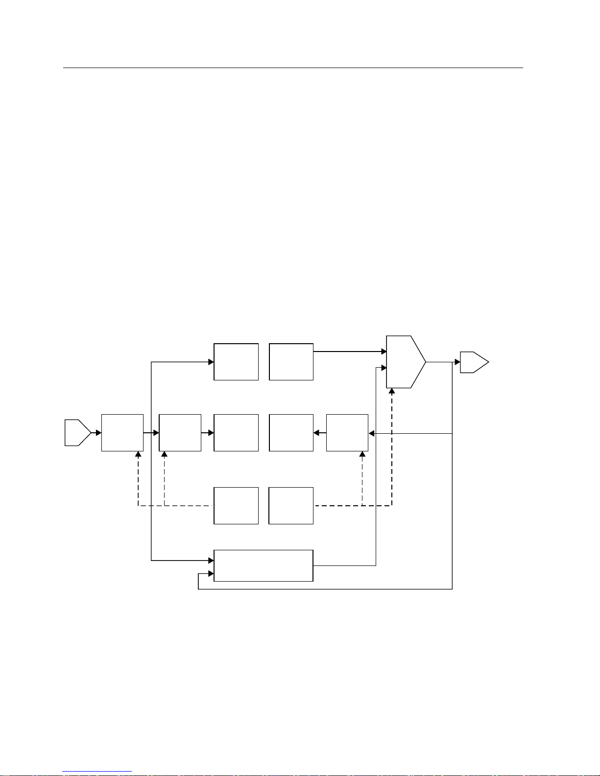
1.3 Aufbau der DIO-Baugruppe
Die DIO-Baugruppe besteht aus drei Hauptteilen:
● Input
● Output
● Counter
,QSXW
,13,)
,13,))
,13,)5
,QYHUVLRQ
,QSXWILOWHU
(GJH
GHWHFWLRQ
,QSXW
LQWHUUXSW
UHJLVWHUV
,QSXW
UHJLVWHU
,13
,13[&
,QSXW
FRQILJXUDWLRQ
UHJLVWHU
2XWSXW
LQWHUUXSW
UHJLVWHUV
2XWSXW
UHJLVWHU
2873
2873[&
2XWSXW
FRQILJXUDWLRQ
UHJLVWHU
2XWSXW
(GJH
GHWHFWLRQ
6RXUFH
VHOHFWLRQ
,QYHUVLRQ
PRGH
2873,)
2873,))
2873,)5
&RXQWHU 7LPHUEORFN
&[&5&[65&[95&[75
&[&205&[5(/5&[&$35
,13[&,19
,13[&(1)
,13[&)7+5(6
,13[&)65$7(
,13[&(15(,
,13[&(1)(,
2873[&(15(,
2873[&(1)(,
2873[&66(/
2873[&202'(
2873[&'02'(
2873[&,19
Page 9

Überblick
1.3 Aufbau der DIO-Baugruppe
SIMATIC PCIe DIO4
Kompaktbetriebsanleitung, 11/2011, A5E03493449-01
7
1.3.1 Input
Der Eingangsteil jedes Eingangs besteht aus einem Filterblock und der Flankenerkennung.
Zusätzlich kann das Eingangssignal invertiert werden: INPxC.INV.
Eingangsfilter
Der optional einschaltbare Filter INPxC.ENF besitzt folgende Eigenschaften:
● Eine Sample-Frequenz mit einer Sample-Periode von 65,5 μs bis 4 ms in Schritten von
65,5 μs, einstellbar über INPxC.FSRATE.
● Einen Sample-Threshold von 1, 3, 5 oder 7 Samples, einstellbar über INPxC.FTHRES.
Die Sample-Frequenz bestimmt, in welchem Abstand der Eingang abgetastet wird. Der
Sample-Threshold bestimmt, wie viele Samples den gleichen Wert haben müssen, bis das
Eingangssignal eindeutig ist und durchgereicht wird. Für die Sample-Frequenz gilt: f
s
=
62,5 MHz / (INPxC.FSRATE << 12).
Beispiel:
● Sample-Periode von 1 ms: INPxC.FSRATE = 0xF
● Sample-Threshold von 5: INPxC.FTHRES = 0x02
Das Eingangssignal muss für mindestens 5 ms den gleichen Pegel haben, bis das
Eingangssignal durchgereicht wird.
Eingangsinterrupts
Für jeden Eingang lassen sich Interrupts bei steigender, fallender oder bei beiden Flanken
des Eingangssignals konfigurieren:
● INPxC.ENREI aktiviert einen Interrupt bei steigender Flanke.
● INPxC.ENFEI aktiviert einen Interrupt bei fallender Flanke.
Wenn einer oder beide Interrupts aktiviert sind und eine Flanke detektiert wird, geschieht
Folgendes:
● Die entsprechenden Bits in INPIF, INPIFR und INPIFF werden gesetzt.
● Das Input-Interrupt-Flag in GSR.IIF wird aktiviert.
Wenn folgende Bedingungen erfüllt sind, löst die DIO dann einen Interrupt aus:
● Die Eingangsinterrupts GCR.IIEN sind aktiviert.
● Die Interrupts GCR.IEN sind freigegeben.
Die Software kann dann die Quelle INPIF, INPIFR, INPIFF feststellen und muss die
entsprechenden Interrupts durch Schreiben der Bits in INPIF, INPIFR oder INPIFF löschen.
Page 10

Überblick
1.3 Aufbau der DIO-Baugruppe
SIMATIC PCIe DIO4
8 Kompaktbetriebsanleitung, 11/2011, A5E03493449-01
1.3.2 Output
Der Ausgangsteil besteht aus folgenden Komponenten:
● Dem Selektor für die Quelle des Ausgangssignals OUTPxC.SSEL.
● Modus-Filtern OUTPxC.DMODE und OUTPxC.OMODE
● Der Flankenerkennung für Interrupts.
Ausgangsquelle
Im Defaultmodus oder nach einem Reset steht die Quelle jedes Ausgangs auf das
entsprechende Bit im Ausgangs-Register OUTP. Durch das Setzen oder Löschen der Bits in
OUTP lassen sich die Ausgänge direkt steuern. Durch die Wahl einer anderen Quelle lassen
sich andere Funktionen implementieren z. B. PWM.
Ausgangsinterrupts
Für jeden Ausgang lassen sich Interrupts bei steigender, fallender oder bei beiden Flanken
des Ausgangssignals konfigurieren:
● OUTPxC.ENREI aktiviert einen Interrupt bei steigender Flanke.
● OUTPxC.ENFEI aktiviert einen Interrupt bei fallender Flanke.
Wenn einer oder beide Interrupts aktiviert sind und eine Flanke detektiert wird, geschieht
Folgendes:
● Die entsprechenden Bits in OUTPIF, OUTPIFR und OUTPIFF werden gesetzt.
● Das Output-Interrupt-Flag in GSR.OIF wird aktiviert.
Wenn folgende Bedingungen erfüllt sind, löst die DIO dann einen Interrupt aus:
● Die Ausgangsinterrupts GCR.OIEN sind aktiviert.
● Die Interrupts GCR.IEN sind freigegeben.
Die Software kann dann die Quelle OUTPIF, OUTPIFR, OUTPIFF feststellen und muss die
entsprechenden Interrupts durch Schreiben der Bits in OUTPIF, OUTPIFR oder OUTPIFF
löschen.
Page 11
Überblick
1.3 Aufbau der DIO-Baugruppe
SIMATIC PCIe DIO4
Kompaktbetriebsanleitung, 11/2011, A5E03493449-01
9
1.3.3 Counter
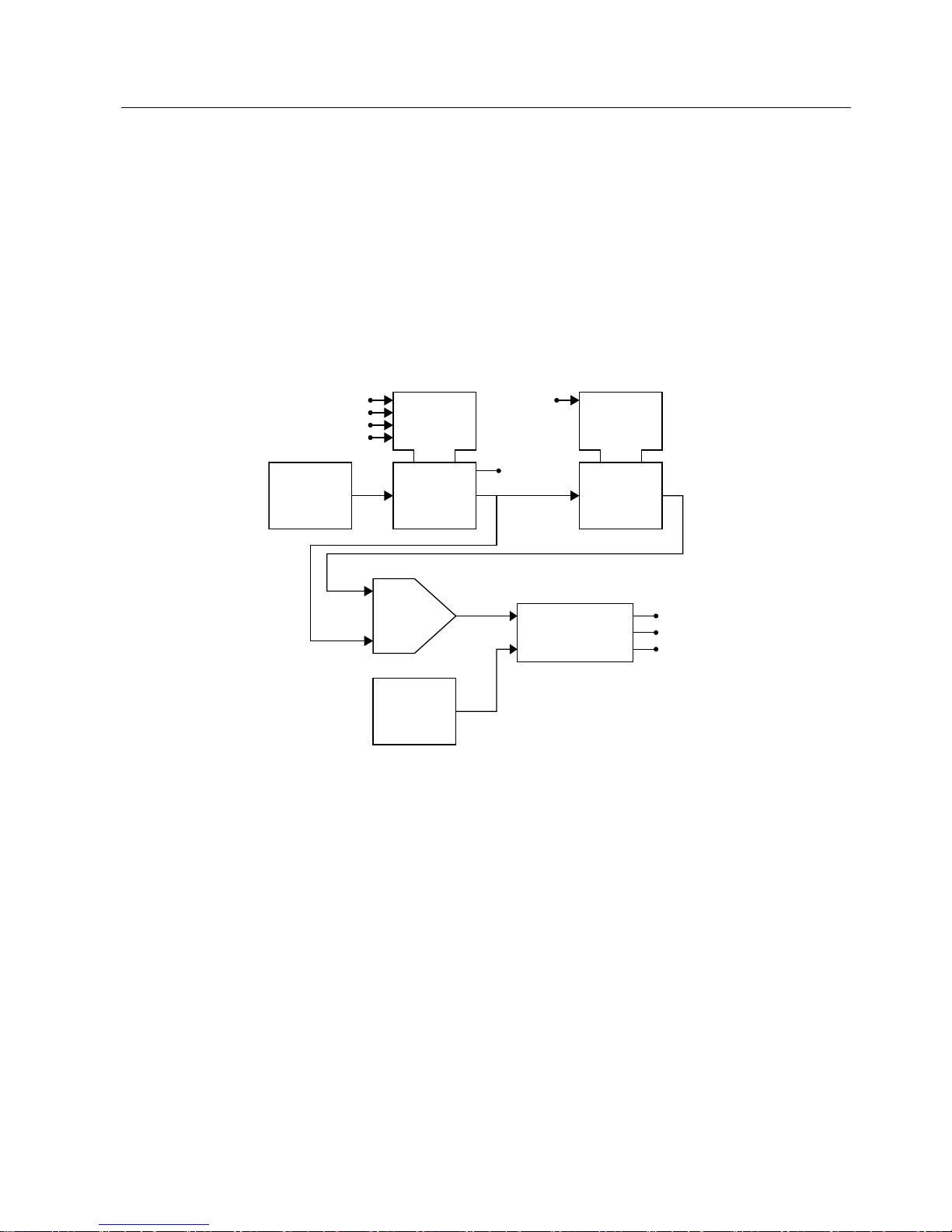
Jeder Zähler (engl. Counter) lässt sich universell durch die Programmierung von SteuerEreignissen (engl. Events) einsetzen. Jeder Counter besitzt folgende Hauptbestandteile:
● Counter: CxVR enthält den aktuellen Counterwert, steuerbar durch die Events "Up"
(CxTR0), "Down" (CxTR1), "Clear" (CxTR2), "Reload" (CxTR3).
● Reload: CxRELR enthält den Reload-Wert.
● Capture: CxCAPR enthält den Capture-Wert, steuerbar durch den Event "Capture"
(CxTR4).
● Compare: CxCOMR enthält den Compare-Wert.
&[&5&6(/
&RPSDUH
VHOHFWLRQ
&[&205
&RPSDUH
UHJLVWHU
$
%
$ %
&RPSDUDWRU
$!%
$%
&[65&(
&[65&*
&[65&6
&[652,)
&DSWXUH
UHJLVWHU
&[&$35
&DSWXUH&[75
&RXQWHU
UHJLVWHU
2YHUIORZ
&[95
8S
'RZQ
&OHDU
5HORDG
5HORDG
UHJLVWHU
&55
&[75
&[75
&[75
&[75
Counter
Der Counter ist ein 36-Bit-Zähler, der mit einem Takt von 62,5 MHz betrieben wird. Bei
andauerndem Hochzählen läuft der Counter nach ca. 1099,5 s über. Der Überlauf wird durch
das Setzen von CxSR.OIF signalisiert.
Der aktuelle Wert des Counter- oder Capture-Registers, auswählbar über CxSR.CSEL, wird
mit dem Compare-Register verglichen. Das Ergebnis gleich, größer oder kleiner wird über
CxSR.CE, CxSR.CG oder CxSR.CS abgebildet.
Der Counter kann Interrupts bei Counter-Overflow und Compare-Events auslösen.
Page 12

Überblick
1.3 Aufbau der DIO-Baugruppe
SIMATIC PCIe DIO4
10 Kompaktbetriebsanleitung, 11/2011, A5E03493449-01
Events
Durch die konfigurierbaren Steuer-Ereignisse (Events) lässt sich der Counter in
verschiedenen Modi betreiben. Jede Eventkette besteht dabei aus folgenden Teilen:
● Quellenauswahl CxTRx.SSEL
● Detektierungsmodus CxTRx.DMODE
● Teiler CxTR0.PEN/CxTRx.PRE
● Ausgangs-Modus CxTRx.OMODE
6RXUFH
VHOHFWLRQ
/HYHO
KLJK
/HYHO
ORZ
(GJH
ULVLQJ
(GJH
IDOOLQJ
%RWK
HGJHV
,QSXW
Q
7RJ J OH
PRGH
1RUPDO
PRGH
,Q 2XW
(YHQW
RXWSXW
(YHQW
VRXUFHV
'HWHFWPRGH
3UHVFDOHU 2XWSXWPRGH
Event-Wirkung
● Event "Up" (CxTR0): Der Counter wird inkrementiert.
● Event "Down" (CxTR1): Der Counter wird dekrementiert.
● Event "Clear" (CxTR2): Der Counter wird gelöscht (0).
● Event "Reload" (CxTR3): Der Wert aus dem Reload-Register CxRELR wird in das
Counter-Register CxVR geladen.
● Event "Capture" (CxTR4): Der aktuelle Counterwert aus CxVR wird im Capture-Register
CxCAPR gespeichert.
Page 13

SIMATIC PCIe DIO4
Kompaktbetriebsanleitung, 11/2011, A5E03493449-01
11
DIO-Baugruppe einbauen und anschließen
2
2.1 Wichtiger Einbauhinweis
VORSICHT
Beschädigung der DIO-Baugruppe beim Einbau
Die 24 V-Versorgungsspannung der DIO-Baugruppe besitzt keinen Verpolschutz. Beim
Verpolen wird intern eine Sicherung ausgelöst, welche die Baugruppe außer Betrieb setzt.
Achten Sie beim Einbau darauf, dass die DIO-Baugruppe korrekt gesteckt ist (digitale Einund Ausgänge außen). Falls Sie doch die DIO-Baugruppe verkehrt stecken und
versehentlich in Betrieb nehmen: ziehen Sie die Baugruppe ab und senden Sie sie zur
Reparatur ein.
2.2 Stromversorgung für die Ausgänge anschließen
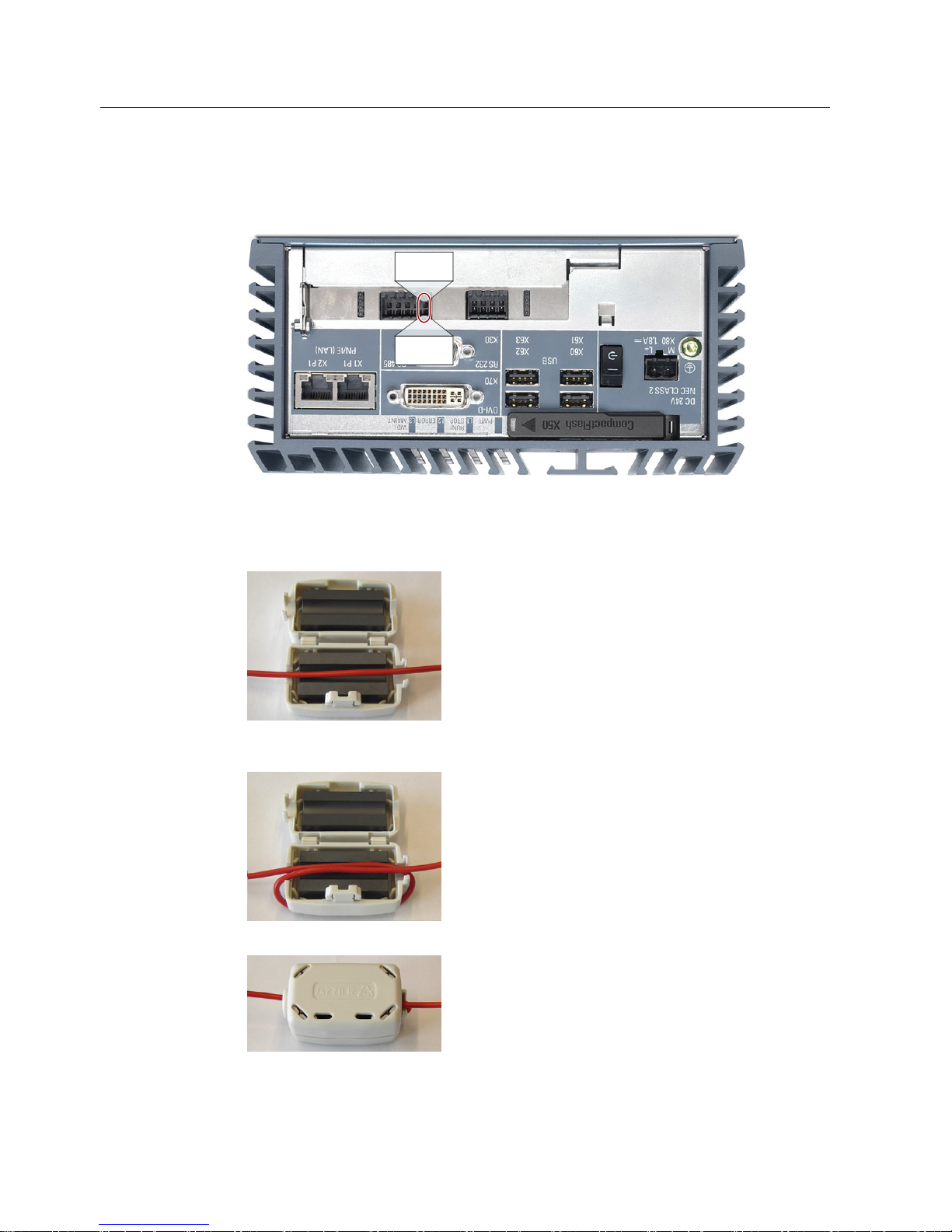
Für die +24 V-Stromversorgungsleitung benötigen Sie den mitgelieferten Klapp-Ferrit der
Firma Würth, Bestellnummer 742711112.
ACHTUNG
Gehäuse des Klapp-Ferrit nicht schließen
Wenn das Gehäuse des Klapp-Ferrit einmal geschlossen ist, dann kann es nicht mehr
geöffnet werden.
Lassen Sie das Gehäuse des Klapp-Ferrit zunächst geöffnet.
Page 14
DIO-Baugruppe einbauen und anschließen
2.2 Stromversorgung für die Ausgänge anschließen
SIMATIC PCIe DIO4
12 Kompaktbetriebsanleitung, 11/2011, A5E03493449-01
Vorgehensweise
1. Verbinden Sie den +24V-Anschluss der Stromversorgung für die Ausgänge mit Pin 10
"P24V_EXT".
3LQ
0B287
3LQ
39B(;7
2. Verbinden Sie den Masseanschluss der Stromversorgung für die Ausgänge mit Pin 9
"M_OUT".
3. Führen Sie die +24 V-Stromversorgungsleitung für die Ausgänge durch das geöffnete
Gehäuse des mitgelieferten Klapp-Ferrit.
4. Führen Sie die +24 V-Stromversorgungsleitung einmal um das Gehäuse des Klapp-Ferrit
herum.
5. Schließen Sie das Gehäuse des Klapp-Ferrit.
Page 15
SIMATIC PCIe DIO4
Kompaktbetriebsanleitung, 11/2011, A5E03493449-01
13
Technische Angaben
3
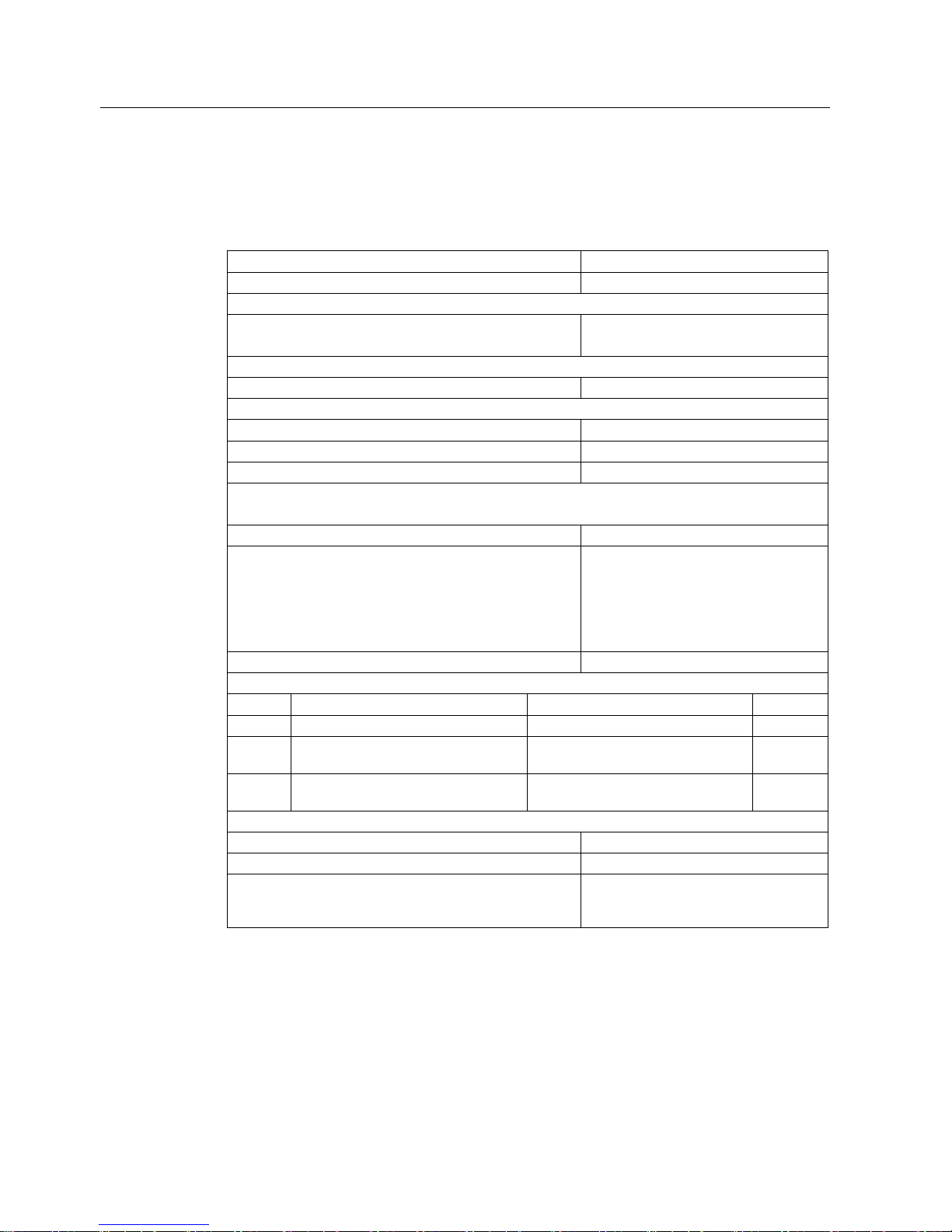
3.1 Anschlussbelegung
+/('B287
+/('B287
+/('B287
+/('B287
+/('B,1
+/('B,1
+/('B,1
+/(' B,1
3LQ
287
3LQ
0B287
3LQ
287
3LQ
0B287
3LQ
287
3LQ
0B287
3LQ
287
3LQ
0B287
3LQ
39B(;7
3LQ
0B287
3LQ
,1
3LQ
0B,1
3LQ
,1
3LQ
0B,1
3LQ
,1
3LQ
0B,1
3LQ
,1
3LQ
0B,1
0B,1 SRWHQ]LDOJHWUHQQWHV0*1'
0B287 0*1'GHU$XVJ¦QJH
39B(;7 9(LQVSHLVXQJI¾UGLH$XVJ¦QJH
Page 16
Technische Angaben
3.2 Technische Daten
SIMATIC PCIe DIO4
14 Kompaktbetriebsanleitung, 11/2011, A5E03493449-01
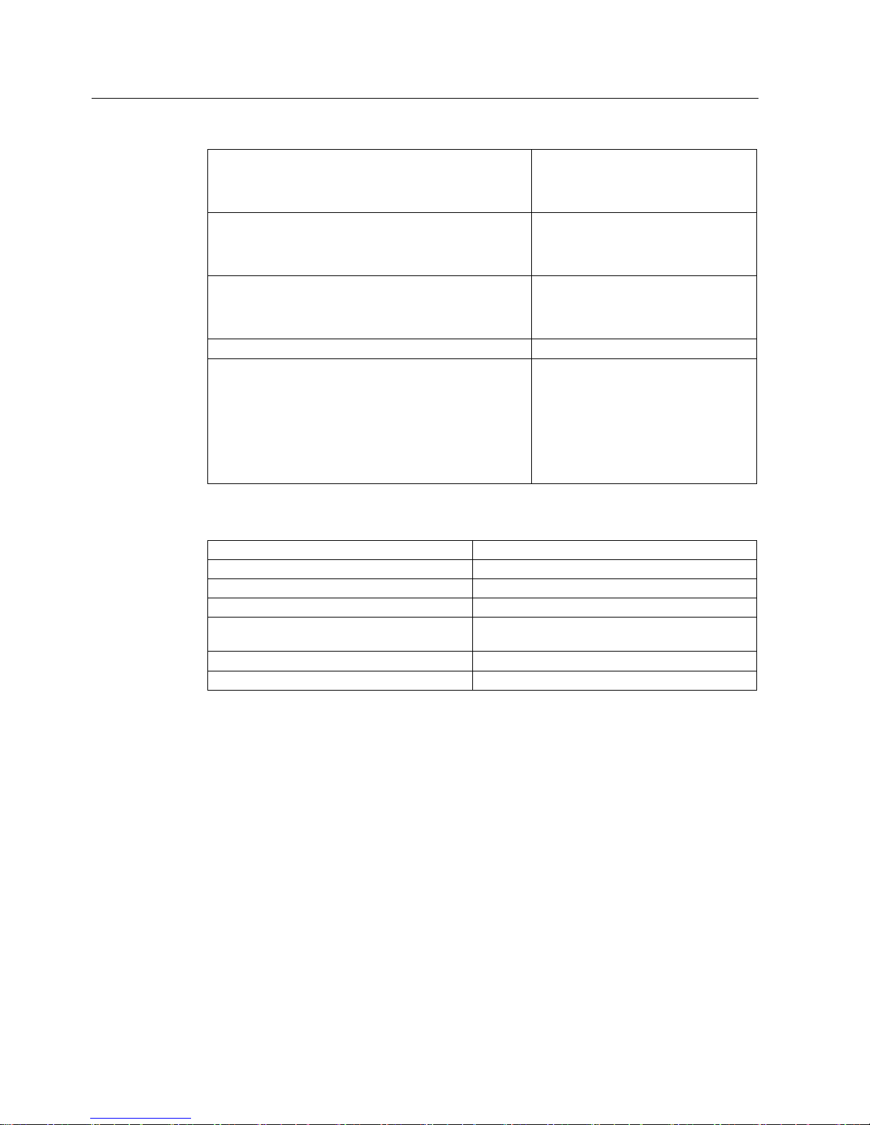
3.2 Technische Daten
Allgemeine technische Daten
Abmessungen B x H x T 101 x 120 x 24 mm
Gewicht ca. 60 g
Versorgungsspannung
P24V_EXT
Zulässiger Spannungsbereich
DC 24 V, NEC class 2
19,2 ... 28,8 V
Stromversorgung/Eingang/Eingangsstrom
Aus Lastspannung L+ (ohne Last) max. 40 mA
Stomaufnahme, Verlustleistung, Potenziale, Isolationsprüfung
Stromaufnahme aus PCIe x1: 3,3 V/12 V 240 mA
Verlustleistung, typisch 3,5 W
Isolation geprüft mit DC 500 V
Elektromagnetische Verträglichkeit
Die Gerätevariante G-IO erfüllt folgende Anforderungen:
Einsatzbereich Industriebereich
Störaussendung EN 61000-6-4:2007
Die Anforderungen der Norm EN 61000-
6-3:2007, Fachgrundnormen-
Störaussendung für Wohnbereich,
Geschäfts- und Gewerbebereiche sowie
Kleinbetriebe werden nicht erfüllt.
Störfestigkeit: EN 61000-6-2:2005
Komponenten für den Überspannungsschutz
Lfd. Nr. Leitung für Komponente
1)
Artikel-Nr.
1 Versorgung UN = DC 24 V BLITZDUCTOR® VT, BVT AD 24 918 402
2 Eingänge von digitalen Baugruppen
UN = DC 24 V
DEHNconnect RK, DCO RK ME 24
(IL = 0,5 A)
919 921
3 Ausgänge von digitalen Baugruppen
UN = DC 24 V
DEHNconnect RK, DCO RK D 5 24
(IL = 10,0 A)
919 986
Status, Alarme, Diagnosen
Statusanzeige Orange LED pro Kanal
Alarme Nein
Diagnosefunktionen Ja; Meldungen bei Spannungsausfall,
Überlast, Temperaturüberschreitung der
Ausgänge
1)
Komponenten der Baureihe BLITZDUCTOR® XT sind mit entsprechendem Zubehör
fernüberwachbar. Weitere Informationen unter http://www.dehn.de. Direktbezug der Bauteile
über: DEHN+SÖHNE GMBH+CO.KG., Hans-Dehn-Str. 1, D-92318 Neumarkt, Tel. +49
(0)9181-906-730
Page 17

Technische Angaben
3.2 Technische Daten
SIMATIC PCIe DIO4
Kompaktbetriebsanleitung, 11/2011, A5E03493449-01
15
Digitaleingänge
Anzahl der Eingänge 4, gleichzeitig ansteuerbar
Eingangsfrequenz maximal 1 kHz
Erforderlicher Stecker 8-polig, Weidmueller B2L 3.50/08/180
SN BK BX; Bestellnr.: 1727650000
Querschnitt der Anschlussleitungen am Stecker 0,08 mm2...1,3 mm2
Eingänge Interruptfähig Ja; auf steigende Flanke, fallende
Flanke oder beide Flanken
Potenzialtrennung zwischen den Kanälen Nein
Eingangsspannung
Nennwert
Für Signal "0"
Für Signal "1"
DC 24 V
-3...+5 V
+15...30 V
Eingangsstrom für Signal "1", typisch 7 mA
Eingangsverzögerung bei Eingangsspannung Nennwert
Einstellbare Filterzeiten pro Eingang
Einstellbare Hysterese pro Eingang
65,5 μs ... 4 ms, Schrittweite 65,5 μs
1, 3, 5 oder 7 Samples
Statusanzeige orange LED pro Kanal
Ansteuerung über Logik; nicht direkt am
Eingangssignal angeschlossen
Digitalausgänge
Anzahl der Ausgänge 4
Erforderlicher Stecker 10-polig, Weidmueller B2L 3.50/10/180
SN BK BX; Betsllnr: 1727660000
Querschnitt der Anschlussleitungen am Stecker 0,08 mm2...1,3 mm2
Ausgänge Interruptfähig Ja; auf steigende Flanke, fallende
Flanke oder beide Flanken
Integrierte Sicherung Ja; 3,15 A
Potenzialtrennung zwischen den Kanälen Nein
Kurzschlussschutz
Ansprechschwelle, typisch
Ja; elektronisch
0,6 A
Begrenzung der induktiven Abschaltspannung auf L+ (-53 V)
Lampenlast nicht zulässig
Ansteuern eines Digitaleingangs
Hinweis: Da der Ausgang nicht "0" treibt, kann der
Wechsel von "1" auf "0" bei hochohmigen Eingängen sehr
lange dauern.
Ja
An jedem Ausgang ist auf der
Baugruppe ein 100 K-Pulldown-
Widerstand angeschlossen.
Ausgangsstrom
Für Signal "1", Nennwert
Für Signal "1", Mindestlaststrom
Für Signal "0", Reststrom
0,5 A
5 mA
0,5 mA
Summenstrom der Ausgänge bis 50 °C max. 2 A
Page 18
Technische Angaben
3.2 Technische Daten
SIMATIC PCIe DIO4
16 Kompaktbetriebsanleitung, 11/2011, A5E03493449-01
Ausgangsverzögerung bei ohmscher Last
"0" nach "1"
"1" nach "0"
max. 100 μs
max. 500 μs
Parallelschalten von 2 Ausgängen
Zur Leistungserhöhung
Zur redundanten Ansteuerung einer Last
Nein
Ja; nur Ausgänge der gleichen Gruppe
Schaltfrequenz
Bei ohmscher Last
Bei induktiver Last
max. 100 Hz
max. 0,5 Hz
Lastwiderstandsbereich 48 Ω ... 4 kΩ
Ausgänge haben einen definierten Zustand
Nach einem Reset: Ausgänge sind
NULL (Low).
Bei System-Stillstand/Absturz:
Ausgänge bleiben im letzten
eingestellten Zustand und können
über Geräte-Watchdog rückgesetzt
werden.
Zähler
Anzahl der Zähler 8
Auflösung 36 Bit, 16 ns
Verknüpfung der Eingänge mit Zähler Beliebig
Verknüpfung der Ausgänge mit Zähler Beliebig
Zählerfunktionen PWM, Pulsbreiten-/Frequenzmessung, Zähler
aufwärts, abwärts, löschen, laden, ...
Anzahl Vergleicher pro Zähler 1
Interruptfähigkeit pro Zähler Überlauf, Vergleich kleiner/größer/gleich
Page 19

SIMATIC PCIe DIO4
Kompaktbetriebsanleitung, 11/2011, A5E03493449-01
17
Beispiele und Registerbelegungen
4
4.1 DIO initialisieren und freigeben
DIO aktivieren
Um die DigitalIO-Baugruppe, kurz DIO, zu aktivieren, gehen Sie wie folgt vor:
1. Mappen Sie den MMIO-Speicherbereich aus BAR0, im Folgenden BASE genannt.
2. Überprüfen Sie die Version und der Eigenschaften der DIO aus dem Register VER:
BASE + 0x0000:
– Version = VER & 0xFF
– Revision = (VER >> 8) & 0xFF
– NumberOfInputs = (VER >> 16) & 0x1F
– NumberOfOutputs = (VER >> 21) & 0x1F
– NumberOfTimers = (VER >> 26) & 0x1F
3. Akquirieren Sie das INUSE-Flags: InUse = (GSR & 1)
Das INUSE-Flag verhindert, dass mehrere Software-Kompenenten gleichzeitig auf die
DIO zugreifen. Bevor eine Software auf die DIO zugreift, muss die Software über das
INUSE-Flag prüfen, ob die Baugruppe bereits in Verwendung ist. Beim ersten Lesen des
Global Status-Registers GSR muss das INUSE-Bit "0" ergeben. Alle weiteren LeseZugriffe ergeben "1". Die DIO ist in Verwendung.
4. Setzen Sie GCR.EN. Die DIO wird aktiviert und die 24 V-Ausgänge eingeschaltet.
Wenn Sie GCR.EN löschen (0), werden alle internen Register zurückgesetzt.
Die Software nutzt nun die DIO für ihren Programmablauf.
DIO deaktivieren
Löschen Sie GCR.EN. Die internen Register werden zurückgesetzt und die 24 V-Ausgänge
abgeschaltet.
DIO freigeben
Schreiben Sie das INUSE-Flag GSR.INUSE. Dadurch wird das INUSE-Flag zurückgesetzt.
Page 20

Beispiele und Registerbelegungen
4.2 Beispiele
SIMATIC PCIe DIO4
18 Kompaktbetriebsanleitung, 11/2011, A5E03493449-01
4.2 Beispiele
Beispiel 1: Eingangsfilter für Eingang 2 setzen
Eingang 2 soll mit einer Periode von 1 ms und einem Schwellwert von 3 abgetastet werden.
Damit ergeben sich folgende Werte:
● INP2C.FSRATE = 0xF
● INP2C.FTHRES = 0x1
● INP2C.ENF = 1
INP2C = 0x3D02
● Konfigurationsadresse berechnen: INP2C = BASE + 0x200 + (2 * 8) = BASE + 0x210.
● Programmieren Sie INP2C mit "0x3D02".
Beispiel 2: Eingang 2 einlesen
Der aktuelle Eingangswert (nach optionaler Filterung und Invertierung) befindet sich im
Register INP (BASE + 0x100), Bit 2.
Beispiel 3: Ausgang 1 setzen
Ausgang 1 lässt sich über OUTP (BASE + 0x400), Bit 1 steuern, sofern die
Ausgangskonfiguration für Ausgang 1 an Adresse
OUTP1C (BASE + 0x500 + (1 * 8) = BASE + 0x508) nicht gändert worden ist.
Beispiel 4: Interrupt bei steigender Flanke an Eingang 0 auslösen
Bei steigender Flanke an Eingang 0 soll ein Interrupt ausgelöst werden. Aktivieren Sie den
entsprechenden Eingangsinterrupt und die globalen Interrupts wie folgt:
● Berechnen Sie die Konfigurationsadresse:
INP0C =BASE + 0x200 + (0 * 8) = BASE + 0x200
● Aktivieren Sie den Eingangsinterrupt bei steigender Flanke:
Setzen Sie INP0C.ENREI, INP0C |= 0x04
● Aktivieren Sie Eingangsinterrupts und globale Interrupts:
Setzen Sie GCR.IIEN und GCR.IEN, GCR |= 0x06
Beispiel 5: Behandlung eines eingehenden Interrupts
Bei einem eingehenden Interrupt empfiehlt sich folgende Vorgehensweise:
Ermitteln Sie die Interrupt-Quelle durch Lesen von GSR (GSR.IIF, GSR.OIF, GSR.CIF,
GSR.EIF):
● GSR.IIF: Werten Sie INPIF, INPIFR und INPIFF aus und löschen Sie diese InterruptFlags durch Schreiben (INPIF = INPIF löscht alle Eingangsinterrupts).
● GSR.OIF: Werten Sie OUTPIF, OUTPIFR und OUTPIFF aus und löschen Sie diese
Interrupt-Flags durch Schreiben (OUTPIF = OUTPIF löscht alle Ausgangsinterrupts).
Page 21

Beispiele und Registerbelegungen
4.2 Beispiele
SIMATIC PCIe DIO4
Kompaktbetriebsanleitung, 11/2011, A5E03493449-01
19
● GSR.CIF: Auswerten von CxSR.IF. Werten Sie CxSR.OIF, CxSR.CEIF, CxSR.CGIF und
CxSR.CSIF aus und löschen Sie diese Interrupts durch Schreiben.
● GSR.EIF: Externer Fehler aufgetreten z. B. fehlende Ausgangsspannung oder
Überlast/Kurzschluss: Beheben Sie den Fehler und löschen Sie GSR.EIF durch
Schreiben.
Überprüfen Sie GSR.IF, ob alle Interrupts abgearbeitet wurden.
Beispiel 6: Frequenz an Eingang 3 messen
In diesem Beispiel wird Counter 3 (C3) verwendet, um die Frequenz von Eingang 3 zu
messen. Als Zeitpunkt wird die steigende Flanke verwendet. Programmieren Sie C3 wie
folgt:
Inkrementierend, Clear + Capture bei steigender Flanke von Eingang 3.
● C3-Adresse berechnen: C3BASE = BASE + 0x1000 + (3 * 0x100) = BASE + 0x1300.
● Event "Up" programmieren: C3TR0 = 0x0100 (Source 0x01 = Always on)
● Event "Clear" programmieren: C3TR2 = 0x2B08 (Source 0x2B = Eingang 3, 0x08 =
Steigende Flanke)
● Event "Capture" programmieren: C3TR4 = 0x2B08 (Source 0x2B = Eingang 3, 0x08 =
Steigende Flanke)
● C3 aktivieren: C3CR.EN |= 1
Die Frequenz berechnet sich dann wie folgt: f
3
=1 / ( (C3CAPR +1) * 16 ns)
Beispiel 7: Pulslänge an Eingang 2 messen
In diesem Beispiel wird Counter 1 (C1) verwendet, um die Pulslänge des Signals an Eingang
2 zu messen. Programmieren Sie C1 wie folgt:
Inkrementierend, Clear bei steigender Flanke, Capture bei fallender Flanke von Eingang 2.
● C1-Adresse berechnen: C1BASE = BASE + 0x1000 + (1 * 0x100) = BASE + 0x1100.
● Event "Up" programmieren: C1TR0 = 0x0100 (Source 0x01 = Always on)
● Event "Clear" programmieren: C1TR2 = 0x2A08 (Source 0x2A = Eingang 2, 0x08 =
Steigende Flanke)
● Event "Capture" programmieren: C1TR4 = 0x2A0A (Source 0x2A = Eingang 2, 0x0A =
Fallende Flanke)
● C1 aktivieren: C1CR.EN |= 1
Die Pulslänge berechnet sich dann wie folgt: t
pw2
= (C1CAPR + 1) * 16 ns
Page 22

Beispiele und Registerbelegungen
4.3 Register
SIMATIC PCIe DIO4
20 Kompaktbetriebsanleitung, 11/2011, A5E03493449-01
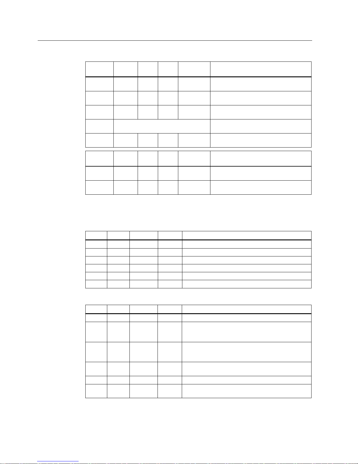
4.3 Register
In den Beschreibungen der Register werden folgende Abkürzungen verwendet:
● RO = Read Only. Nur Lesezugriff.
● RW = Read, Write. Lese- und Schreibzugriff
● RWC = Read, Write/Clear. Lesezugriff. Ein Schreibvorgang löscht das entsprechende Bit.
Block Addesse Größe
(Bit)
Zugriff Register Beschreibung
General BASE +
0x0000
32 RO VER Version: ID/Version/Capabilities
BASE +
0x0004
32 RW GCR General Control-Register: Global Enable,
Global Interrupt Enable, ...
BASE +
0x0008
32 RWC GSR General Status-Register: INUSE-Flag,
Global Interrupt-Flag, ...
Input BASE +
0x0100
32 RO INP Eingänge 0-31 Aktueller Wert des
Eingangssignals (nach dem Eingangsfilter)
BASE +
0x0110
32 RWC INPIF Eingänge 0-31 Interrupt-Flags, Input
Interrupt-Flags
BASE +
0x0120
32 RWC INPIFR Eingänge 0-31 Interrupt-Flags (steigende
Flanke)
BASE +
0x0130
32 RWC INPIFF Eingänge 0-31 Interrupt-Flags (fallende
Flanke)
BASE +
0x0200
64 RW INP0C Konfiguration von Eingang 0: Filter,
Invertierung, Interrupt, ..
BASE +
0x0208
64 RW INP1C Konfiguration von Eingang 1: Filter,
Invertierung, Interrupt, ..
BASE +
0x0210
64 RW INP2C Konfiguration von Eingang 2: Filter,
Invertierung, Interrupt, ..
BASE +
0x0218
64 RW INP3C Konfiguration von Eingang 3: Filter,
Invertierung, Interrupt, ..
... 64 RW INPnC Konfiguration von Eingang n: Filter,
Invertierung, Interrupt, ..
BASE +
0x02F8
64 RW INP31C Konfiguration von Eingang 31: Filter,
Invertierung, Interrupt, ..
Output BASE +
0x0400
32 RW OUTP Ausgang 0-31 Werte
BASE +
0x0410
32 RWC OUTPIF Ausgänge 0-31 Interrupt-Flags
BASE +
0x0420
32 RWC OUTPIFR Ausgänge 0-31 Interrupt-Flags (steigende
Flanke)
BASE +
0x0430
32 RWC OUTPIFF Ausgänge 0-31 Interrupt-Flags (fallende
Flanke)
BASE +
0x0500
64 RW OUTP0C Konfiguration von Ausgang 0: Invertierung,
Quelle, ...
BASE +
0x0508
64 RW OUTP1C Konfiguration von Ausgang 1: Invertierung,
Quelle, ...
Page 23

Beispiele und Registerbelegungen
4.3 Register
SIMATIC PCIe DIO4
Kompaktbetriebsanleitung, 11/2011, A5E03493449-01
21
Block Addesse Größe
(Bit)
Zugriff Register Beschreibung
BASE +
0x0510
64 RW OUTP2C Konfiguration von Ausgang 2: Invertierung,
Quelle, ...
BASE +
0x0518
64 RW OUTP3C Konfiguration von Ausgang 3: Invertierung,
Quelle, ...
... 64 RW OUTPnC Konfiguration von Ausgang n: Invertierung,
Quelle, ...
BASE +
0x05F8
64 RW OUTP31C Konfiguration von Ausgang 31: Invertierung,
Quelle, ...
Counter 0 BASE +
0x1000
32 RW C0CR Counter 0 Control-Register
BASE +
0x1008
32 RW C0SR Counter 0 Status-Register
BASE +
0x1010
56 RO C0VR Counter 0 Value-Register
BASE +
0x1020
32 RW C0TR0 Counter 0 Trigger-Register 0 ("Up")
BASE +
0x1028
32 RW C0TR1 Counter 0 Trigger-Register 1 ("Down")
BASE +
0x1030
32 RW C0TR2 Counter 0 Trigger-Register 2 ("Clear")
BASE +
0x1038
32 RW C0TR3 Counter 0 Trigger-Register 3 ("Reload")
BASE +
0x1040
32 RW C0TR4 Counter 0 Trigger-Register 4 ("Capture")
BASE +
0x1060
56 RW C0COMR Counter 0 Compare-Register
BASE +
0x1070
56 RW C0RELR Counter 0 Reload-Register
BASE +
0x1078
56 RW C0CAPR Counter 0 Capture-Register
Counter 1 BASE +
0x1100
32 RW C1CR Counter 1 Control-Register
BASE +
0x1108
32 RW C1SR Counter 1 Status-Register
BASE +
0x1110
56 RO C1VR Counter 1 Value-Register
BASE +
0x1120
32 RW C1TR0 Counter 1 Trigger-Register 0 ("Up")
BASE +
0x1128
32 RW C1TR1 Counter 1 Trigger-Register 1 ("Down")
BASE +
0x1130
32 RW C1TR2 Counter 1 Trigger-Register 2 ("Clear")
BASE +
0x1138
32 RW C1TR3 Counter 1 Trigger-Register 3 ("Reload")
BASE +
0x1140
32 RW C1TR4 Counter 1 Trigger-Register 4 ("Capture")
Page 24
Beispiele und Registerbelegungen
4.3 Register
SIMATIC PCIe DIO4
22 Kompaktbetriebsanleitung, 11/2011, A5E03493449-01
Block Addesse Größe
(Bit)
Zugriff Register Beschreibung
BASE +
0x1160
56 RW C1COMR Counter 1 Compare-Register
BASE +
0x1170
56 RW C1RELR Counter 1 Reload-Register
BASE +
0x1178
56 RW C1CAPR Counter 1 Capture-Register
Counter n Die Register wiederholen sich
entsprechend.
Siehe Beschreibung oben.
Counter 7 BASE +
0x1778
56 RW C7CAPR Counter 7 Capture-Register
Block Addesse Größe
(Bit)
Zugriff Register Beschreibung
BASE +
0x4040
32 RO PCIEIS PCIe core Interrupt Status Register
BASE +
0x4050
32 RW PCIEIE PCIe core Interrupt Enable Register
General-Register
VER: Version (BASE + 0x0000)
Bit Zugriff Name Default Beschreibung
31 RO 0 Reserviert
30..26 RO NRCT 8 Anzahl Zähler/Zeitgeber
25..21 RO NROP 4 Anzahl Ausgangssignale
20..16 RO NRIP 4 Anzahl Eingangssignale
15..8 RO REV 00 Revision
7..0 RO VER 10 Version des DIO-Interface (1.0)
GCR: General Control-Register (BASE + 0x0004)
Bit Zugriff Name Default Beschreibung
31..10 RO 0 Reserviert
9 RW GATERST 0 Wenn "1", wird der externe Reset deaktiviert (gated), so
dass die DIO ihren Betrieb weiter führt, selbst wenn das
System neu startet.
8 RW ENLOOP 0 Aktiviert den Loopback-Modus. Wenn "1", werden alle
Eingänge intern mit den Ausgangs-Registern verbunden.
Die Ausgangssignale verändern nicht ihren letzten Wert.
7 RW EIEN 0 Error-Interrupt aktiviert. Wenn "1" und GSR.EIF = 1, wird
GSR.IF gesetzt.
6..5 RO 0 Reserviert
4 RW CIEN 0 Counter-Interrupt aktiviert. Wenn "1" und GSR.CIF = 1,
wird GSR.IF gesetzt.
Page 25
Beispiele und Registerbelegungen
4.3 Register
SIMATIC PCIe DIO4
Kompaktbetriebsanleitung, 11/2011, A5E03493449-01
23
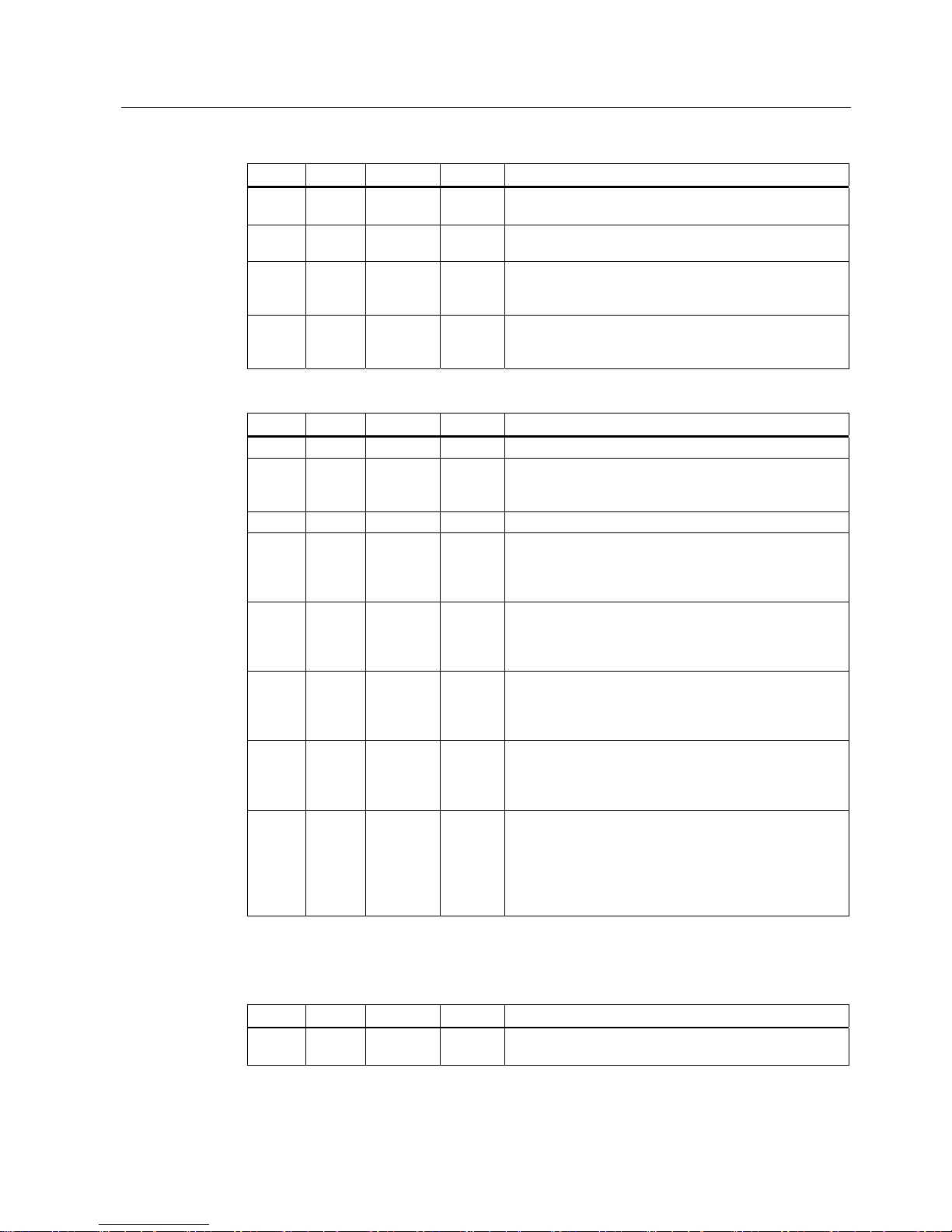
Bit Zugriff Name Default Beschreibung
3 RW OIEN 0 Ausgangsinterrupt aktiviert. Wenn "1" und GSR.OIF = 1,
wird GSR.IF gesetzt.
2 RW IIEN 0 Eingangsinterrupt aktiviert. Wenn "1" und GSR.IIF = 1,
wird GSR.IF gesetzt.
1 RW IEN 0 Global-Interrupt aktiviert. Wenn "1", werden Interrupts
aktiviert. Wenn STATUS.IF = 1, wird ein Interrupt
ausgelöst.
0 RW EN 0 Global aktiviert. Muss auf "1" gesetzt sein, damit ein
normaler Betrieb möglich ist. Wenn auf "0" gesetzt,
werden alle internen Register zurückgesetzt.
GSR: General Status-Register (BASE + 0x0008)
Bit Zugriff Name Default Beschreibung
31..8 RO 0 Reserviert
7 RWC EIF 0 Error Interrupt-Flag. Wenn "1", ist ein Fehler aufgetreten.
Wenn das Bit mit "1" beschrieben wird, wird das Bit
zurückgesetzt.
6..5 RO 0 Reserviert
4 RO CIF 0 Counter Interrupt-Flag. Wenn dieses Flag gesetzt wurde,
hat ein Zähler einen Interrupt ausgelöst. Wenn alle
aktivierten Counter-Interrupts gelöscht werden, wird das
Bit zurückgesetzt.
3 RO OIF 0 Output Interrupt-Flag. Wenn dieses Flag gesetzt wurde,
hat ein Ausgang einen Interrupt ausgelöst. Wenn alle
aktivierten Ausgangsinterrupts gelöscht werden, wird das
Bit zurückgesetzt.
2 RO IIF 0 Eingang Interrupt-Flag. Wenn dieses Flag gesetzt wurde,
hat ein Eingang einen Interrupt ausgelöst. Wenn alle
aktivierten Eingangsinterrupts gelöscht werden, wird das
Bit zurückgesetzt.
1 RO IF 0 Interrupt-Flag. Wenn EIF, CIF, OIF oder IIF = 1, wird das
Flag gesetzt. Um dieses Bit zu löschen, müssen alle
Interrupts gelöscht werden. Wenn das Bit gesetzt ist und
CONTROL.IEN =1, wird ein Interrrupt ausgelöst.
0 RWC INUSE 0 Das Bit ergibt "0" beim ersten Lesen des Global Status-
Registers GSR. Alle weiteren Lese-Zugriffe ergeben "1".
Die DIO ist in Verwendung.
Das INUSE-Flag kann benutzt werden, damit mehrere
Treiber auf die DIO zugreifen können. Wenn das Bit mit
"1" beschrieben wird, wird das Bit zurückgesetzt.
Eingangs-Register
INP: Eingangs-Register (BASE + 0x0100)
Bit Zugriff Name Default Beschreibung
31..0 RO INx - Jedes Bit spiegelt den entsprechenden Eingang wieder,
nach Filterung und Invertierung.
Page 26

Beispiele und Registerbelegungen
4.3 Register
SIMATIC PCIe DIO4
24 Kompaktbetriebsanleitung, 11/2011, A5E03493449-01
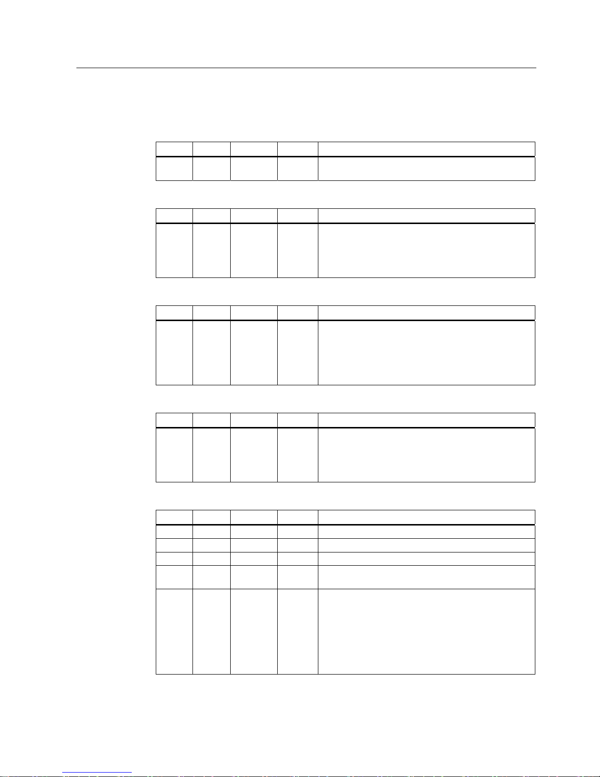
INPIF: Eingangsinterrupt-Flag-Register (BASE + 0x0110)
Bit Zugriff Name Default Beschreibung
31..0 RWC IFx 0 Jedes Bit spiegelt den Interruptzustand des
entsprechenden Eingangs wieder. Wenn ein Bit gesetzt
wird, wird STATUS.IIF gesetzt. Wenn das Bit mit "1"
beschrieben wird, wird das Bit zurückgesetzt, ebenfalls
die entsprechenden IFRE/IFFE-Bits.
INPIFR: Eingangsinterrupt-Flag-Register, steigende Flanke (BASE + 0x0120)
Bit Zugriff Name Default Beschreibung
31..0 RWC IFREx 0 Jedes Bit spiegelt den Interruptzustand steigender
Flanke des entsprechenden Eingangs wieder. Wenn ein
Bit gesetzt wird, wird STATUS.IIF gesetzt. Wenn das Bit
gesetzt wird, wird das entsprechende INPUTIF.IF
gesetzt. Wenn das Bit mit "1" beschrieben wird, wird das
Bit zurückgesetzt.
INPIFF: Eingangsinterrupt-Flag-Register, fallende Flanke (BASE + 0x0130)
Bit Zugriff Name Default Beschreibung
31..0 RWC IFFEx 0 Jedes Bit spiegelt den Interruptzustand fallender Flanke
des entsprechenden Eingangs wieder. Wenn das Bit
gesetzt wird, wird das entsprechende INPUTIF.IF
gesetzt. Wenn das Bit mit "1" beschrieben wird, wird das
Bit zurückgesetzt.
INPxC: Eingang x Configuration-Register (BASE + 0x0200 + (x*8))
Bit Zugriff Name Default Beschreibung
63..16 RO 0 Reserviert
15..10 RW FSRATE 0 Sample-Frequenz Eingangsfilter fs = 62,5 MHz /
(FSRATE << 12).
9..8 RW FTHRES 0 Sample-Threshold Eingangsfilter. 00: 1 Sample, 01: 3
Samples, 10: 5 Samples, 11: 7 Samples.
7..4 RO 0 Reserviert
3 RW ENFEI 0 Aktiviert einen Interrupt bei fallender Flanke des
Eingangssignals. Wenn das Bit gesetzt ist und eine
fallende Flanke am Eingang detektiert wird, wird das
entsprechende Bit in INPIFF.IFFE gesetzt.
2 RW ENREI 0 Aktiviert einen Interrupt bei steigender Flanke des
Eingangssignals. Wenn das Bit gesetzt ist und eine
steigende Flanke am Eingang detektiert wird, wird das
entsprechende Bit in INPIFR.IFRE gesetzt.
1 RW ENF 0 Aktiviert den Eingangsfilter. Wenn "1", wird der Eingang
gefiltert mit den Einstellungen von FSRATE und
FTHRES.
0 RW INV 0 Wenn "1", wird das Eingangssignal invertiert, bevor es
weiter verarbeitet wird.
Page 27
Beispiele und Registerbelegungen
4.3 Register
SIMATIC PCIe DIO4
Kompaktbetriebsanleitung, 11/2011, A5E03493449-01
25
Ausgangs-Register
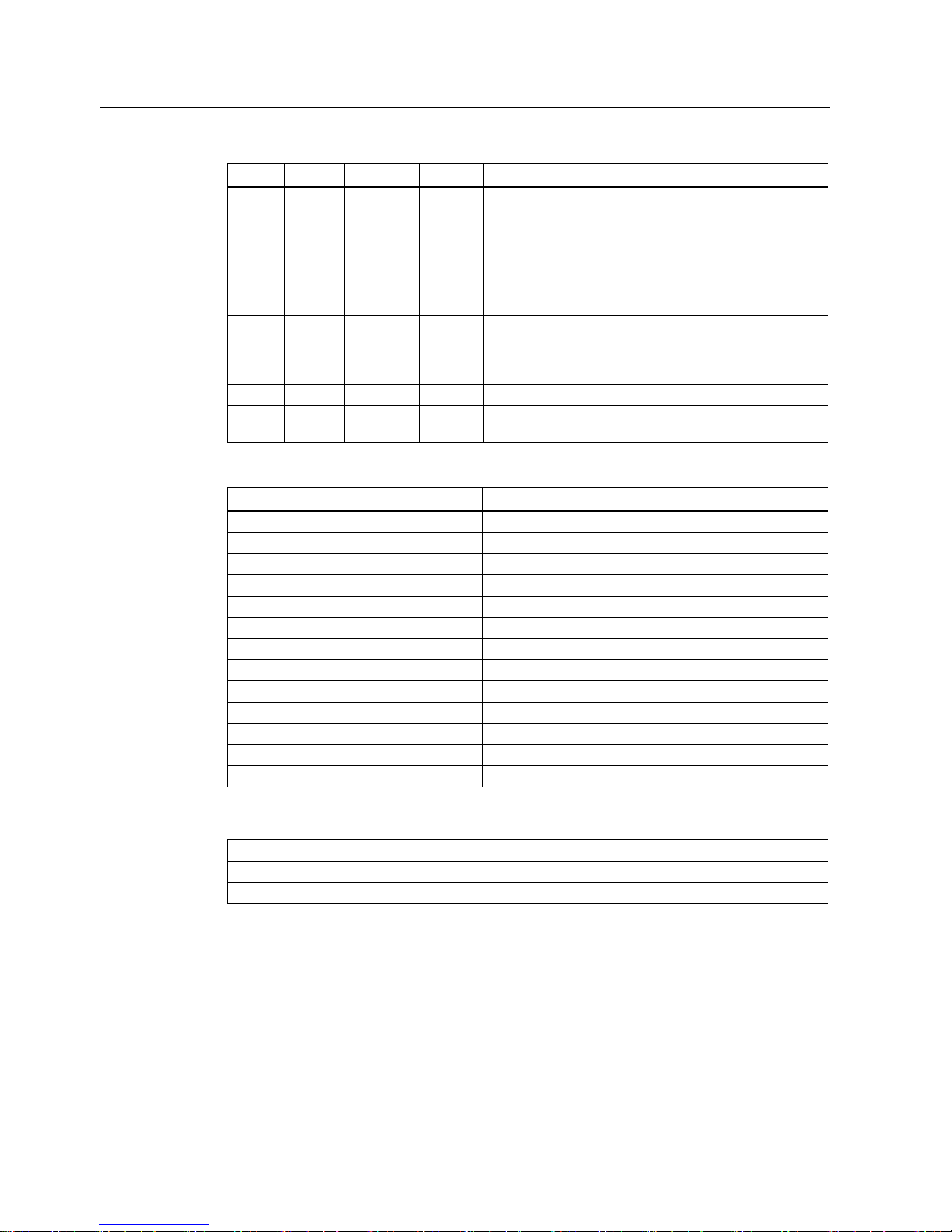
OUTP: Ausgangs-Register (BASE + 0x0400)
Bit Zugriff Name Default Beschreibung
31..0 RW OUTx - Jedes Bit spiegelt den entsprechenden Ausgangswert im
Default-Modus (OUTPxC.SSEL = 0).
OUTPIF: Output Interrupt-Flag-Register (BASE + 0x0410)
Bit Zugriff Name Default Beschreibung
31..0 RWC IFx 0 Jedes Bit spiegelt den Interruptzustand des
entsprechenden Ausgangs wieder. Wenn ein Bit gesetzt
wird, wird STATUS.OIF gesetzt. Wenn das Bit mit "1"
beschrieben wird, wird das Bit zurückgesetzt, ebenfalls
die entsprechenden IFRE/IFFE-Bits.
OUTPIFR: Output Interrupt-Flag-Register, steigende Flanke (BASE + 0x0420)
Bit Zugriff Name Default Beschreibung
31..0 RWC IFREx 0 Jedes Bit spiegelt den Interruptzustand "Steigende
Flanke" des entsprechenden Ausgangs wieder. Wenn
ein Bit gesetzt wird, wird STATUS.IIF gesetzt. Wenn das
Bit gesetzt wird, wird das entsprechende OUTPIF.IF
gesetzt. Wenn das Bit mit "1" beschrieben wird, wird das
Bit zurückgesetzt.
OUTPIFF: Output Interrupt-Flag-Register, fallende Flanke (BASE + 0x0430)
Bit Zugriff Name Default Beschreibung
31..0 RWC IFFEx 0 Jedes Bit spiegelt den Interruptzustand "Fallende
Flanke" des entsprechenden Ausgangs wieder. Wenn
das Bit gesetzt wird, wird das entsprechende OUTPIF.IF
gesetzt. Wenn das Bit mit "1" beschrieben wird, wird das
Bit zurückgesetzt.
OUTP0C: Ausgang x Configuration-Register (BASE + 0x0500 + (x*8))
Bit Zugriff Name Default Beschreibung
63..46 RO 0 Reserviert
45..40 RW SSEL 0 Wahl der Ausgangsquelle, siehe "Ausgangsquellen"
39..38 RO 0 Reserviert
37..36 RW OMODE 0 Wahl des Ausgang-Modus: 00: Normal, 01 = Wechselnd
(1→0, 0→1)
35..33 RW DMODE 0 Wahl des Ausgang-Detect-Modus:
000: hoher Level
001: niedriger Level
100: nur steigende Flanke
101: nur fallende Flanke
110: steigende und fallende Flanke
Page 28
Beispiele und Registerbelegungen
4.3 Register
SIMATIC PCIe DIO4
26 Kompaktbetriebsanleitung, 11/2011, A5E03493449-01
Bit Zugriff Name Default Beschreibung
32 RO OS 0 Status der Ausgangswahl. Wenn "1", ist der Ausgang
aktiv.
31..4 RO 0 Reserviert
3 RW ENFEI 0 Aktiviert einen Interrupt bei fallender Flanke des
Ausgangssignals. Wenn das Bit gesetzt ist und eine
fallende Flanke am Ausgang detektiert wird, wird das
entsprechende Bit in OUTPIFF.IFFE gesetzt.
2 RW ENREI 0 Aktiviert einen Interrupt bei steigender Flanke des
Ausgangssignals. Wenn das Bit gesetzt ist und eine
steigende Flanke am Ausgang detektiert wird, wird das
entsprechende Bit in OUTPIFR.IFRE gesetzt.
1 RO 0 Reserviert
0 RW INV 0 Wenn "1", wird das Ausgangssignal invertiert, bevor es
weiter verarbeitet wird.
Ausgangsquellen
Werte (dezimal) Ausgangssignal
0 OUTPx
1 1
2 DIO lesen
3 DIO schreiben
4 DIO Interrupt (GSR.IF)
5-7 Reserviert
8/12/16/20/24/28/32/36 Counter x Overflow
9/13/17/21/25/29/33/37 Counter x Vergleich "gleich" (CxSR.CE)
10/14/18/22/26/30/34/38 Counter x Vergleich "größer" (CxSR.CG)
11/15/19/23/27/31/35/39 Counter x Vergleich "kleiner" (CxSR.CS)
40-43 Eingang 0-3 (INP 0..3)
44-47 Ausgang 0-3 (OUTP 0..3)
48-63 Reserviert
Die Werte für den Index von Input, Output und Counter sollten Sie nach folgender Formel
berechnen:
Counter x index Index = 8 + x*4
Input x index Index = 8 + VER.NRCT*4 + x
Output x index Index = 8 + VER.NRCT*4 + VER.NRIP + x
Page 29
Beispiele und Registerbelegungen
4.3 Register
SIMATIC PCIe DIO4
Kompaktbetriebsanleitung, 11/2011, A5E03493449-01
27
Counter-Register
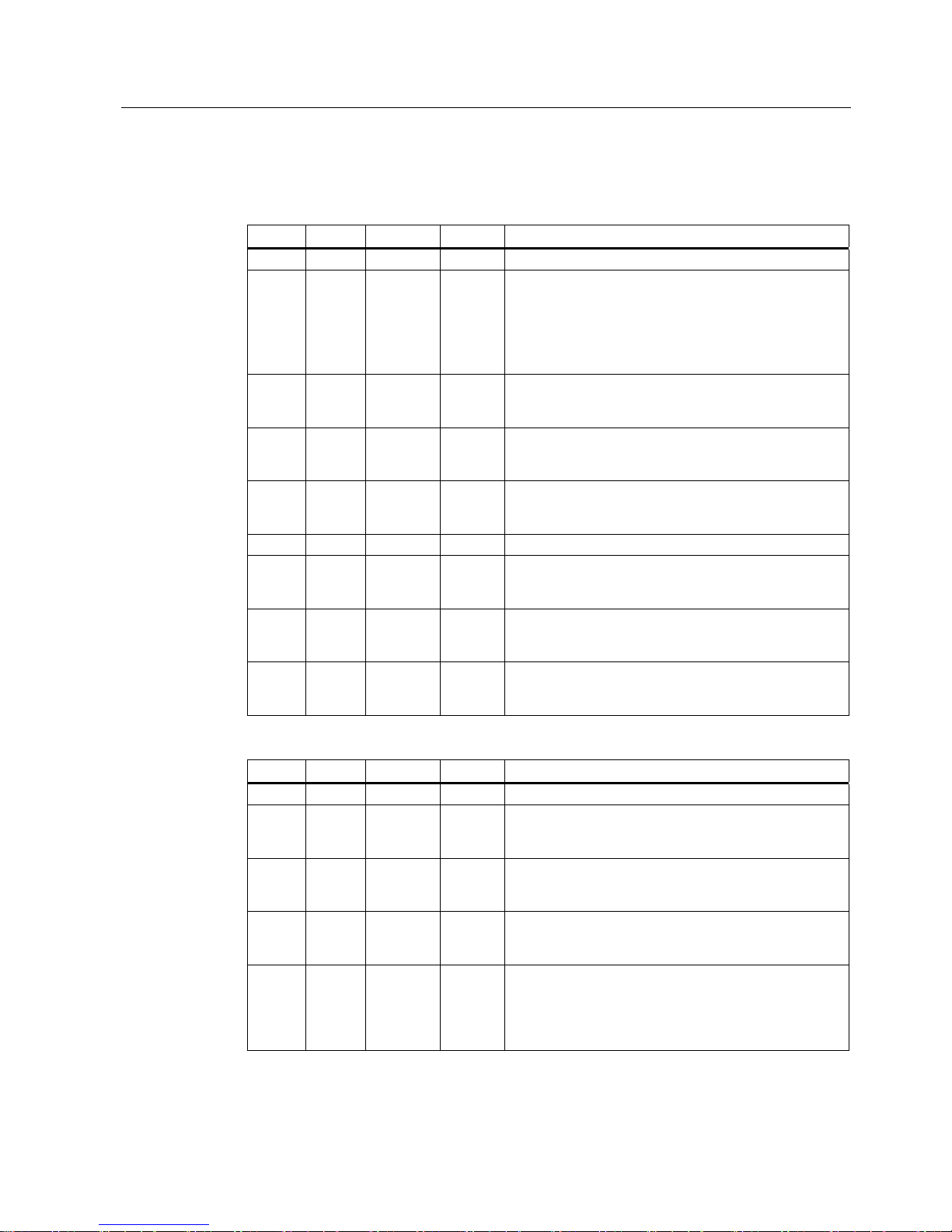
CxCR: Counter x Control-Register (BASE + 0x1000 + (x*0x100))
Bit Zugriff Name Default Beschreibung
31..9 RO 0 Reserviert
8 RW CSEL 0 Wahl des Vergleichs-Registers (Compare).
0: Vergleich des Compare-Registers mit dem
Counter-Register CVR
1: Vergleich des Compare-Registers mit Capture-
Register CAPR
7 RW CSIEN 0 Aktiviert einen Interrupt beim Vergleichs-Ergebnis
"kleiner". Wenn das Bit auf "1" gesetzt ist und
CxSR.CSIF = 1, wird CxSR.IF gesetzt.
6 RW CGIEN 0 Aktiviert einen Interrupt beim Vergleichs-Ergebnis
"größer". Wenn das Bit auf "1" gesetzt ist und
CxSR.CGIF = 1, wird CxSR.IF gesetzt.
5 RW CEIEN 0 Aktiviert einen Interrupt beim Vergleichs-Ergebnis
"gleich". Wenn das Bit auf "1" gesetzt ist und CxSR.CEIF
= 1, wird CxSR.IF gesetzt.
4..3 RO 0 Reserviert
2 RW OIEN 0 Aktiviert einen Interrupt bei Counter-Overflow. Wenn das
Bit auf "1" gesetzt ist und CxSR.OIF = 1, wird CxSR.IF
gesetzt.
1 RW IEN 0 Aktiviert einen Counter-Interrupt. Wenn das Bit auf "1"
gesetzt ist und CxSR.IF = 1, wird ein Counter-Interrupt
ausgelöst.
0 RW EN 0 Aktiviert den Counter. Wenn das Bit auf "1" gesetzt ist,
ist der Zähler in Betrieb. Wenn "0", wird der Zähler
gestoppt und die Counter-Register zurückgesetzt.
CxSR: Counter x Status-Register (BASE + 0x1008 + (x*0x100))
Bit Zugriff Name Default Beschreibung
31..11 RO 0 Reserviert
10 RO CS 0 Flag für Vergleichs-Ergebnis "kleiner". Wenn "1", ist das
gewählte Vergleichs-Registers CxCR.CSEL kleiner als
das Compare-Register.
9 RO CG 0 Flag für Vergleichs-Ergebnis "größer". Wenn "1", ist das
gewählte Vergleichs-Registers CxCR.CSEL größer als
das Compare-Register.
8 RO CE 0 Flag für Vergleichs-Ergebnis "gleich". Wenn "1", ist das
gewählte Vergleichs-Registers CxCR.CSEL gleich dem
Compare-Register.
7 RWC CSIF 0 Interrupt-Flag für Vergleichs-Ergebnis "kleiner". Wenn
"1", wurde ein Interrupt beim Vergleichs-Ergebnis
"kleiner" ausgelöst: CxVR/CxCAPR < CxCOMR. Wenn
das Bit mit "1" beschrieben wird, wird das Bit
zurückgesetzt.
Page 30
Beispiele und Registerbelegungen
4.3 Register
SIMATIC PCIe DIO4
28 Kompaktbetriebsanleitung, 11/2011, A5E03493449-01
Bit Zugriff Name Default Beschreibung
6 RWC CGIF 0 Interrupt-Flag für Vergleichs-Ergebnis "größer". Wenn
"1", wurde ein Interrupt beim Vergleichs-Ergebnis
"größer" ausgelöst: CxVR/CxCAPR > CxCOMR. Wenn
das Bit mit "1" beschrieben wird, wird das Bit
zurückgesetzt.
5 RWC CEIF 0 Interrupt-Flag für Vergleichs-Ergebnis "gleich". Wenn "1",
wurde ein Interrupt beim Vergleichs-Ergebnis "gleich"
ausgelöst: CxVR/CxCAPR == CxCOMR. Wenn das Bit
mit "1" beschrieben wird, wird das Bit zurückgesetzt.
4..3 RO 0 Reserviert
2 RWC OIF 0 Interrupt-Flag für Counter-Overflow. Wenn "1", wurde ein
Interrupt bei Counter-Overflow ausgelöst. Wenn das Bit
mit "1" beschrieben wird, wird das Bit zurückgesetzt.
1 RO IF 0 Interrupt-Flag für Counter. Wenn OIF, CEIF, CGIF oder
CSIF aktiviert wurden und aktiv sind, wird das Flag
gesetzt.
0 RO 0 Reserviert
CxVR: Counter x Wert-Register (BASE + 0x1010 + (x*0x100))
Bit Zugriff Name Default Beschreibung
35..0 RO 0 Aktueller Zähler-Wert
CxTR0: Counter x Trigger-Register 0 (BASE + 0x1020 + (x*0x100))
Wenn der Trigger aktiv ist, wird der Counter inkrementiert.
Bit Zugriff Name Default Beschreibung
31..24 RO 0 Reserviert
23..16 RW PRE 0 Trigger-Vorteiler. Anzahl von Events, bis der Trigger
aktiv wird.
15..14 RO 0 Reserviert
13..8 RW SSEL 0 Wahl der Trigger-Quelle, siehe "Ausgangsquellen".
7 RW PEN 0 Vorteiler aktiviert. Wenn "1", wird der Trigger vorgeteilt
durch den Wert von PRE.
6 RO 0 Reserviert
5..4 RW OMODE 0 Wahl des Trigger-Ausgangs-Modus:
00: Normal
01: Wechselnd (1→0, 0→1)
3..1 RW DMODE 0 Wahl des Trigger-Detect-Modus:
000: hoher Level
001: niedriger Level
100: nur steigende Flanke
101: nur fallende Flanke
110: steigende und fallende Flanke
0 RO TS 0 Trigger-Status. Wenn "1", ist der Trigger aktiv.
Page 31

Beispiele und Registerbelegungen
4.3 Register
SIMATIC PCIe DIO4
Kompaktbetriebsanleitung, 11/2011, A5E03493449-01
29
CxTR1: Counter 0 Trigger-Register 1 (BASE + 0x1028 + (x*0x100))
Wenn der Trigger aktiv ist, wird der Counter dekrementiert, siehe Beschreibung CxTR0.
CxTR2: Counter 0 Trigger-Register 2 (BASE + 0x1030 + (x*0x100))
Wenn der Trigger aktiv ist, wird Counter 0 gelöscht, siehe Beschreibung CxTR0.
CxTR3: Counter 0 Trigger-Register 3 (BASE + 0x1038 + (x*0x100))
Wenn der Reload-Trigger aktiv ist, wird der Counter mit dem Wert von CxRELR
beschrieben, siehe Beschreibung CxTR0.
CxTR4: Counter 0 Trigger-Register 4 (BASE + 0x1040 + (x*0x100))
Wenn der Capture-Trigger aktiv ist, wird der aktuelle Zählwert des Counters in das CaptureRegister CxCAPR geschrieben, siehe Beschreibung CxTR0.
Counter Trigger-Quellen
Wert (dezimal) Signal
0 0
1 1
2 DIO lesen
3 DIO schreiben
4 DIO Interrupt (GSR.IF)
5-7 Reserviert
8/12/16/20/24/28/32/36 Counter x Overflow
9/13/17/21/25/29/33/37 Counter x Vergleich "gleich" (CxSR.CE)
10/14/18/22/26/30/34/38 Counter x Vergleich "größer" (CxSR.CG)
11/15/19/23/27/31/35/39 Counter x Vergleich "kleiner" (CxSR.CS)
40-43 Eingang 0-3 (INP 0..3)
44-47 Ausgang 0-3 (OUTP 0..3)
48-63 Reserviert
Die Werte für den Index von Input, Output und Counter sollten Sie nach folgender Formel
berechnen:
Counter x index Index = 8 + x*4
Input x index Index = 8 + VER.NRCT*4 + x
Output x index Index = 8 + VER.NRCT*4 + VER.NRIP + x
CxCOMR: Counter x Compare-Register (BASE + 0x1060 + (x*0x100))
Bit Zugriff Name Default Beschreibung
35..0 RW CMP 0 Compare value
Page 32
Beispiele und Registerbelegungen
4.3 Register
SIMATIC PCIe DIO4
30 Kompaktbetriebsanleitung, 11/2011, A5E03493449-01
Wenn CxCR.CSEL = "0", wird der Wert des Registers mit CxVR verglichen. Wenn
CxCR.CSEL = "1", wird der Wert des Registers mit CxCAPR verglichen. CxSR enthält das
Vergleichs-Ergebnis:
CxSR.CE CxVR/CxCAPR ist gleich CxCOMR.
CxSR.CG CxVR/CxCAPR ist größer CxCOMR.
CxSR.CS CxVR/CxCAPR ist kleiner CxCOMR.
CxRELR: Counter x Reload-Register (BASE + 0x1070 + (x*0x100))
Wenn der Reload-Trigger CxTR3 aktiv ist, wird das Register in das Counter-Register CxVR
geschrieben.
Bit Zugriff Name Default Beschreibung
35..0 RW REL 0 Reload-Wert
CxCAPR: Counter x Capture-Register (BASE + 0x1078 + (x*0x100))
Wenn der Capture-Trigger CxTR4 aktiv ist, wird der aktuelle Wert von CxVR in diesem
Register gesichert.
Bit Zugriff Name Default Beschreibung
35..0 RW CAP 0 Capture-Wert
PCIEIS: PCIe core Interrupt Status Register (BASE + 0x4040)
Das Register enthält das Interrupt-Statusbit des PCIe-Kernel.
Bit Zugriff Name Default Beschreibung
31...8 RO Reserved
7 RO IA 0 Interrupt active: Wenn dieses Bit gesetzt ist, meldet der
PCIe-Kernel dem System einen Interrupt.
6...0 RO Reserved 0
PCIEIE: PCIe core Interrupt Enable Register (BASE + 0x4050)
Das Register enthält das Interrupt-Enable-Bit des PCIe-Kernel. Alle Bits mit Ausnahme von
Bit 7 müssen erhalten und dauerhaft gesichert werden.
Bit Zugriff Name Default Beschreibung
31...8 RO Reserved
7 RW IE 0 Interrupt enable: Wenn dieses Bit gesetzt ist, leitet der
PCIe-Kernel Interrupts an das System weiter. Wenn
dieses Bit nicht gesetzt ist, wird kein Interrupt erzeugt,
auch nicht wenn GCR.IEN gesetzt ist.
6...0 RO Reserved 0
Page 33

SIMATIC PCIe DIO4
_
_________________
_
_
_________________
_
_
_________________
_
SIMATIC
Industrial PCs
SIMATIC PCIe DIO4
Compact Operating Instructions
11/2011
A5E03493449-01
Overview
1
Installing and connecting the
DIO module
2
Technical specifications
3
Examples and register
assignments
4
Page 34
Legal information
Legal information
Warning notice system
This manual contains notices you have to observe in order to ensure your personal safety, as well as to prevent
damage to property. The notices referring to your personal safety are highlighted in the manual by a safety alert
symbol, notices referring only to property damage have no safety alert symbol. These notices shown below are
graded according to the degree of danger.
DANGER
indicates that death or severe personal injury will result if proper precautions are not taken.
WARNING
indicates that death or severe personal injury may result if proper precautions are not taken.
CAUTION
with a safety alert symbol, indicates that minor personal injury can result if proper precautions are not taken.
CAUTION
without a safety alert symbol, indicates that property damage can result if proper precautions are not taken.
NOTICE
indicates that an unintended result or situation can occur if the relevant information is not taken into account.
If more than one degree of danger is present, the warning notice representing the highest degree of danger will
be used. A notice warning of injury to persons with a safety alert symbol may also include a warning relating to
property damage.
Qualified Personnel
The product/system described in this documentation may be operated only by personnel qualified for the specific
task in accordance with the relevant documentation, in particular its warning notices and safety instructions.
Qualified personnel are those who, based on their training and experience, are capable of identifying risks and
avoiding potential hazards when working with these products/systems.
Proper use of Siemens products
Note the following:
WARNING
Siemens products may only be used for the applications described in the catalog and in the relevant technical
documentation. If products and components from other manufacturers are used, these must be recommended
or approved by Siemens. Proper transport, storage, installation, assembly, commissioning, operation and
maintenance are required to ensure that the products operate safely and without any problems. The permissible
ambient conditions must be complied with. The information in the relevant documentation must be observed.
Trademarks
All names identified by ® are registered trademarks of Siemens AG. The remaining trademarks in this publication
may be trademarks whose use by third parties for their own purposes could violate the rights of the owner.
Disclaimer of Liability
We have reviewed the contents of this publication to ensure consistency with the hardware and software
described. Since variance cannot be precluded entirely, we cannot guarantee full consistency. However, the
information in this publication is reviewed regularly and any necessary corrections are included in subsequent
editions.
Siemens AG
Industry Sector
Postfach 48 48
90026 NÜRNBERG
GERMANY
A5E03493449-01
Ⓟ 12/2011 Technical data subject to change
Copyright © Siemens AG 2011.
All rights reserved
Page 35

SIMATIC PCIe DIO4
Compact Operating Instructions, 11/2011, A5E03493449-01
3
Table of contents
1 Overview.................................................................................................................................................... 5
1.1
Validity............................................................................................................................................5
1.2
Product description ........................................................................................................................5
1.3
Design of the DIO module..............................................................................................................6
1.3.1 Input
...............................................................................................................................................7
1.3.2
Output ............................................................................................................................................8
1.3.3
Counter ..........................................................................................................................................9
2
Installing and connecting the DIO module ............................................................................................... 11
2.1
Important installation note............................................................................................................11
2.2
Connecting the power supply of the outputs................................................................................11
3
Technical specifications........................................................................................................................... 13
3.1
Terminal assignment....................................................................................................................13
3.2
Technical specifications ...............................................................................................................14
4
Examples and register assignments........................................................................................................ 17
4.1
Initializing and enabling DIO ........................................................................................................17
4.2
Examples .....................................................................................................................................18
4.3
Registers......................................................................................................................................20
Page 36

Table of contents
SIMATIC PCIe DIO4
4 Compact Operating Instructions, 11/2011, A5E03493449-01
Page 37
SIMATIC PCIe DIO4
Compact Operating Instructions, 11/2011, A5E03493449-01
5
Overview
1
1.1 Validity
This short description applies to the PCIe DIO4 module for the SIMATIC IPC227D, hereafter
referred to as "DIO module".
This product information includes important information. The information supplements the
operating instructions for the device and take precedence over statements in the operating
instructions, the release notes and the online help.
1.2 Product description
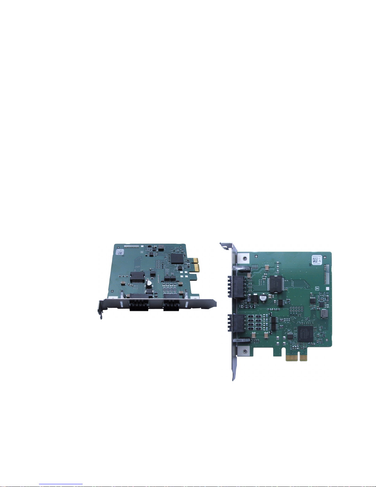
The DIO module is a PCIe x1 module and provides four digital 24 V inputs and four digital
24 V outputs. The DIO module also offers eight hardware-based counters (62.5 MHz base
clock) that can be configured for functions such as PWM, frequency measurement and pulse
width measurement.
All functional units (inputs, outputs, counters) can generate interrupts (rising/falling edges,
counter overflows, zero passage, etc.).
Page 38
Overview
1.3 Design of the DIO module
SIMATIC PCIe DIO4
6 Compact Operating Instructions, 11/2011, A5E03493449-01
Typical area of application
● Reading/writing of digital inputs/outputs
● Interrupt-controlled responding to inputs
● Creating PWM output signal
● Measuring frequencies and pulse lengths
● Counting results and responding interrupt-controlled to counter states, e.g. zero passage,
overflow
1.3 Design of the DIO module
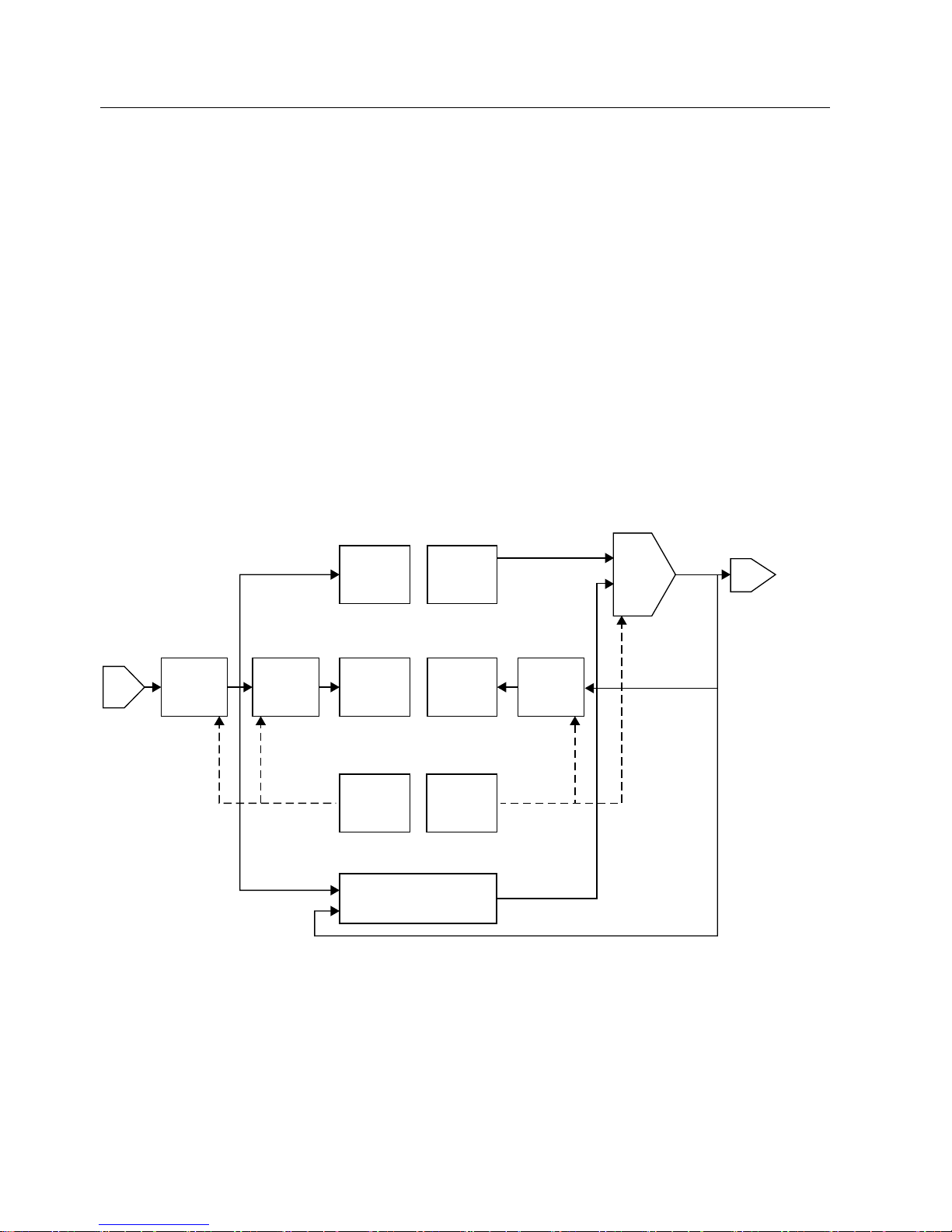
The DIO module consists of three main parts:
● Input
● Output
● Counter
,QSXW
,13,)
,13,))
,13,)5
,QYHUVLRQ
,QSXWILOWHU
(GJH
GHWHFWLRQ
,QSXW
LQWHUUXSW
UHJLVWHUV
,QSXW
UHJLVWHU
,13
,13[&
,QSXW
FRQILJXUDWLRQ
UHJLVWHU
2XWSXW
LQWHUUXSW
UHJLVWHUV
2XWSXW
UHJLVWHU
2873
2873[&
2XWSXW
FRQILJXUDWLRQ
UHJLVWHU
2XWSXW
(GJH
GHWHFWLRQ
6RXUFH
VHOHFWLRQ
,QYHUVLRQ
PRGH
2873,)
2873,))
2873,)5
&RXQWHU 7LPHUEORFN
&[&5&[65&[95&[75
&[&205&[5(/5&[&$35
,13[&,19
,13[&(1)
,13[&)7+5(6
,13[&)65$7(
,13[&(15(,
,13[&(1)(,
2873[&(15(,
2873[&(1)(,
2873[&66(/
2873[&202'(
2873[&'02'(
2873[&,19
Page 39

Overview
1.3 Design of the DIO module
SIMATIC PCIe DIO4
Compact Operating Instructions, 11/2011, A5E03493449-01
7
1.3.1 Input
The input part of each input consists of a filter block and the edge detection. The input signal
can also be inverted: INPxC.INV.
Input filter
The optional available INPxC.ENF filter has the following properties:
● A sample frequency with a sample period of 65.5 μs up to 4 ms in increments of 65.5 μs,
adjustable via INPxC.FSRATE.
● A sample threshold of 1, 3, 5 or 7 samples that can be set by means of INPxC.FTHRES.
The sample frequency determines in which interval the input is sampled. The sample
threshold determines how many samples must have the same value until the input signal is
unique and will be passed through. The following applies to the sample frequency: f
s
=
62.5 MHz / (INPxC.FSRATE << 12).
Example:
● Sample period of 1 ms: INPxC.FSRATE = 0xF
● Sample threshold of 5: INPxC.FTHRES = 0x02
The input signal must have the same level for at least 5 ms until the input signal is passed
through.
Input interrupts
You can configure interrupts for rising, falling or both edges of the input signal for each input:
● INPxC.ENREI enables an interrupt with a rising edge.
● INPxC.ENREI enables an interrupt with a falling edge.
The following happens if one or both interrupts are enabled and an edge is detected:
● The corresponding bits in INPIF, INPIFR and INPIFF are set.
● The input interrupt flag in GSR.IIF is enabled.
If the following conditions are met, the DIO triggers an interrupt:
● The input interrupts GCR.IIEN are enabled.
● The interrupts GCR.IEN are enabled.
The software can detect the source INPIF, INPIFR, INPIFF and must delete the
corresponding interrupts by writing the bits in INPIF, INPIFR or INPIFF.
Page 40

Overview
1.3 Design of the DIO module
SIMATIC PCIe DIO4
8 Compact Operating Instructions, 11/2011, A5E03493449-01
1.3.2 Output
The output part consists of the following components:
● The selector for the source of the OUTPxC.SSEL output signal.
● Mode filters OUTPxC.DMODE and OUTPxC.OMODE
● The edge detection for interrupts.
Output source
The source of each output is set to the respective bit in the OUTP output register in default
mode or after a reset. The outputs can be directly controlled by setting or deleting the bits in
OUTP. Other functions, such as PWM, can be implemented by selecting a different source.
Output interrupts
You can configure interrupts for rising, falling or both edges of the output signal for each
output:
● OUTPxC.ENREI enables an interrupt with a rising edge.
● OUTPxC.ENREI enables an interrupt with a falling edge.
The following happens if one or both interrupts are enabled and an edge is detected:
● The corresponding bits in OUTPIF, OUTPIFR and OUTPIFF are set.
● The output interrupt flag in GSR.OIF is enabled.
If the following conditions are met, the DIO triggers an interrupt:
● The output interrupts GCR.OIEN are enabled.
● The interrupts GCR.IEN are enabled.
The software can detect the source OUTPIF, OUTPIFR, OUTPIFF and must delete the
corresponding interrupts by writing the bits in OUTPIF, OUTPIFR or OUTPIFF.
Page 41
Overview
1.3 Design of the DIO module
SIMATIC PCIe DIO4
Compact Operating Instructions, 11/2011, A5E03493449-01
9
1.3.3 Counter
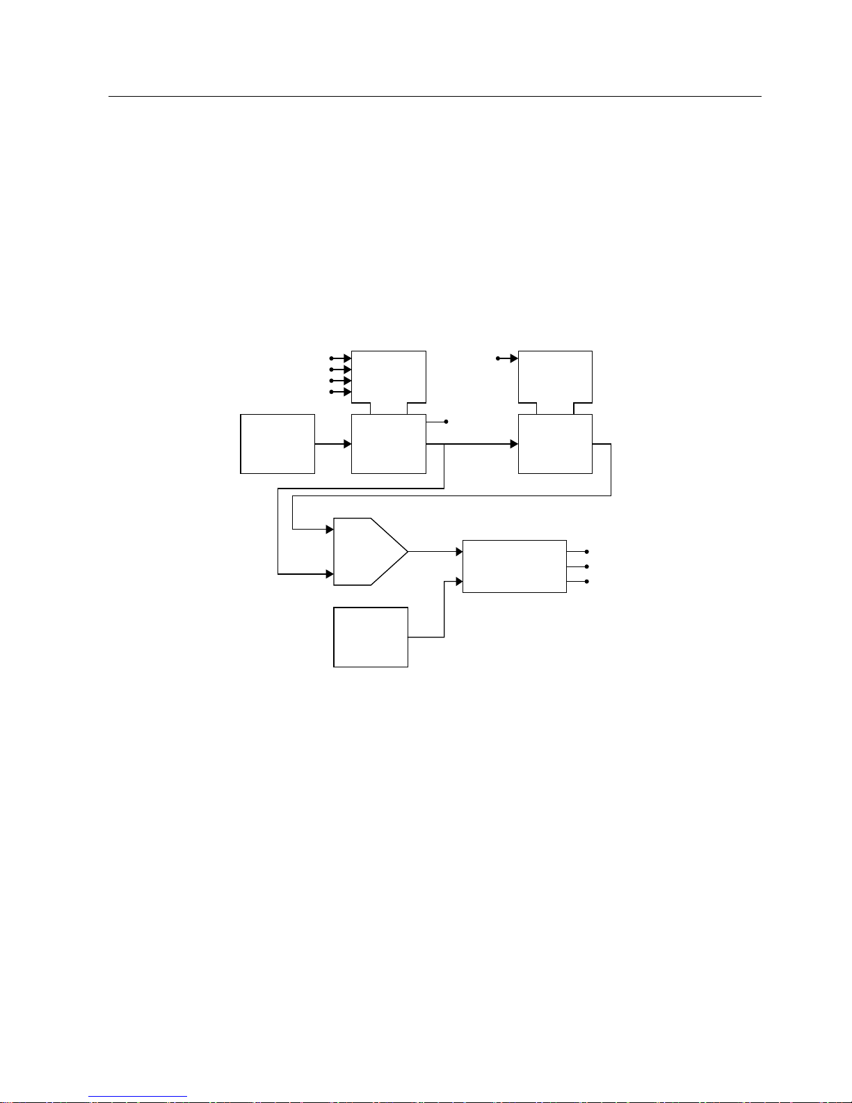
Each counter can be used universally by programming events. Each counter has the
following main components:
● Counter: CxVR includes the current counter value which can be controlled by the events
"Up" (CxTR0), "Down" (CxTR1), "Clear" (CxTR2), "Reload" (CxTR3).
● Reload: CxRELR includes the reload value.
● Capture: CxCAPR includes the capture value and can be controlled with the "Capture"
(CxTR4) event.
● Compare: CxCOMR includes the compare value.
&[&5&6(/
&RPSDUH
VHOHFWLRQ
&[&205
&RPSDUH
UHJLVWHU
$
%
$ %
&RPSDUDWRU
$!%
$%
&[65&(
&[65&*
&[65&6
&[652,)
&DSWXUH
UHJLVWHU
&[&$35
&DSWXUH&[75
&RXQWHU
UHJLVWHU
2YHUIORZ
&[95
8S
'RZQ
&OHDU
5HORDG
5HORDG
UHJLVWHU
&55
&[75
&[75
&[75
&[75
Counter
The counter is a 36-bit counter operated with a cycle of 62.5 MHz. With continuous
incrementing, the counter overflows after about 1099.5 seconds. The overflow is signaled by
setting CxSR.OIF.
The current value of the counter or capture register, which can be selected via CxSR.CSEL,
is compared with the compare register. The result is equal to, greater than or less than and
is mapped by means of CxSR.CE, CxSR.CG or CxSR.CS.
The counter can trigger interrupts in case of counter overflow and compare events.
Page 42
Overview
1.3 Design of the DIO module
SIMATIC PCIe DIO4
10 Compact Operating Instructions, 11/2011, A5E03493449-01
Events
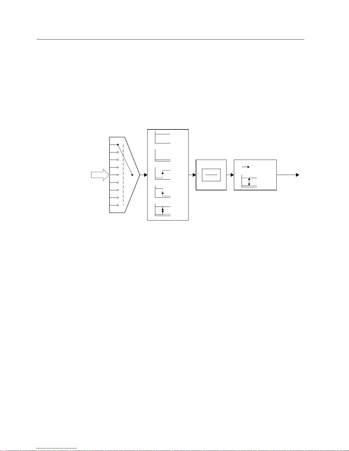
The counter can be operated in different modes because the events are configurable. Each
event chain consists of the following components:
● Source selection CxTRx.SSEL
● Detection mode CxTRx.DMODE
● Divisor CxTR0.PEN/CxTRx.PRE
● Output mode CxTRx.OMODE
6RXUFH
VHOHFWLRQ
/HYHO
KLJK
/HYHO
ORZ
(GJH
ULVLQJ
(GJH
IDOOLQJ
%RWK
HGJHV
,QSXW
Q
7RJ J OH
PRGH
1RUPDO
PRGH
,Q 2XW
(YHQW
RXWSXW
(YHQW
VRXUFHV
'HWHFWPRGH
3UHVFDOHU 2XWSXWPRGH
Event effect
● Event "Up" (CxTR0): The counter is incremented.
● Event "Down" (CxTR1): The counter is decremented.
● Event "Clear" (CxTR2): The counter is deleted (0).
● Event "Reload" (CxTR3): The value from the CxRELR reload register is loaded into the
CxVR counter register.
● Event "Capture" (CxTR4): The current counter value from CxVR is saved in the CxCAPR
capture register.
Page 43

SIMATIC PCIe DIO4
Compact Operating Instructions, 11/2011, A5E03493449-01
11
Installing and connecting the DIO module
2
2.1 Important installation note
CAUTION
Damaging the DIO module during installation
The 24 V supply voltage of the DIO module is not protected against reverse polarity. An
internal safety mechanism is triggered in case of reverse polarity which renders the module
inoperable.
Make sure that the DIO module is installed with correct polarity (digital inputs and outputs
on outside). If you do install the DIO module with reversed polarity and inadvertently take it
into operation: Remove the module and send it in for repair.
2.2 Connecting the power supply of the outputs
You need the supplied clamp-on ferrite core from Würth, order number 742711112, for the
+24 V power supply cable.
NOTICE
Do not close the housing of the clamp-on ferrite core
Once the housing of the clamp-on ferrite core is closed, it cannot be opened again.
First, leave the housing of the clamp-on ferrite core open.
Page 44
Installing and connecting the DIO module
2.2 Connecting the power supply of the outputs
SIMATIC PCIe DIO4
12 Compact Operating Instructions, 11/2011, A5E03493449-01
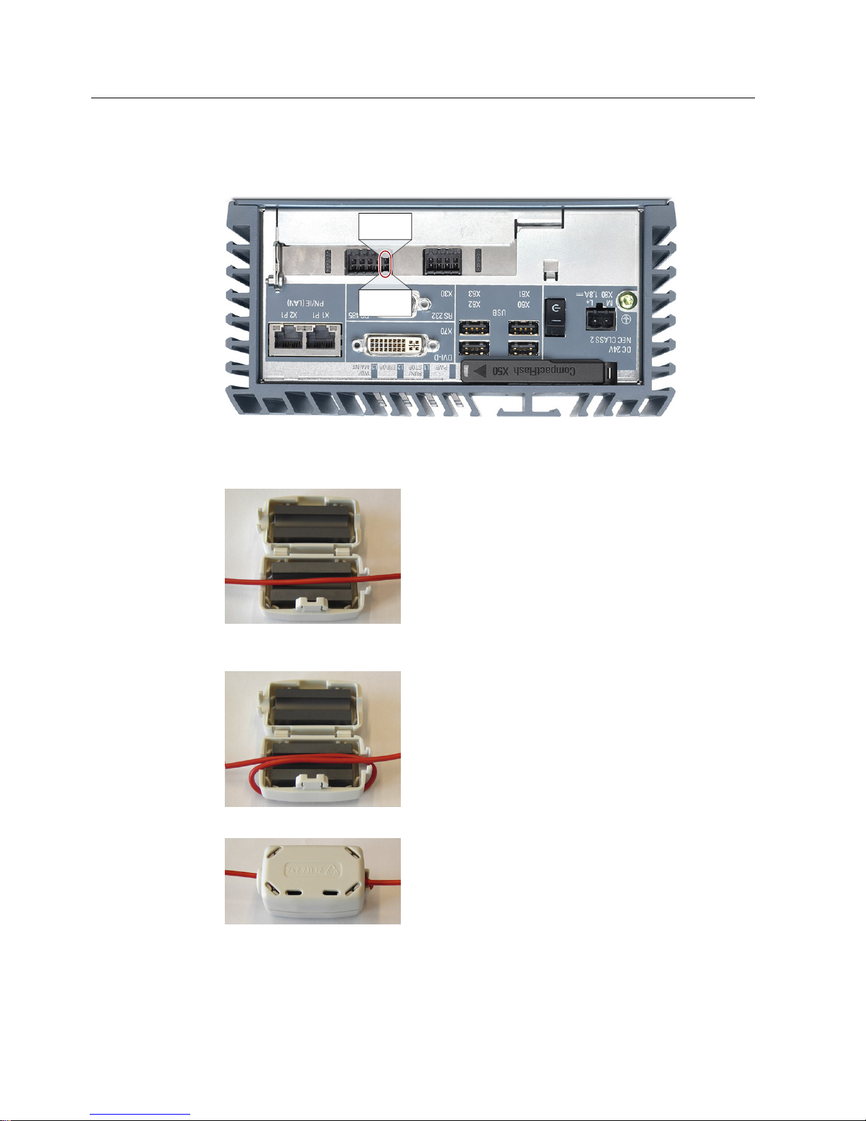
Procedure
1. Connect the +24V connector of the power supply for the outputs with pin 10 "P24V_EXT".
3LQ
0B287
3LQ
39B(;7
2. Connect the ground connector of the power supply for the outputs with pin 9 "M_OUT".
3. Route the +24 V power supply cable for the outputs through the open housing of the
supplied clamp-on ferrite core.
4. Route the +24 V power supply cable once around the housing of the clamp-on ferrite
core.
5. Close the clamp-on ferrite core housing.
Page 45
SIMATIC PCIe DIO4
Compact Operating Instructions, 11/2011, A5E03493449-01
13
Technical specifications
3
3.1 Terminal assignment
+/('B287
+/('B287
+/('B2 87
+/('B287
+/('B,1
+/('B,1
+/('B,1
+/('B,1
3LQ
287
3LQ
0B287
3LQ
287
3LQ
0B287
3LQ
287
3LQ
0B287
3LQ
287
3LQ
0B287
3LQ
39B(;7
3LQ
0B287
3LQ
,1
3LQ
0B,1
3LQ
,1
3LQ
0B,1
3LQ
,1
3LQ
0B,1
3LQ
,1
3LQ
0B,1
0B,1 JDOYDQLFDOO\LVRODWHG0*1'
0B287 0*1'RIRXWSXWV
39B(;7 9VXSSO\IRURXWSXWV
Page 46
Technical specifications
3.2 Technical specifications
SIMATIC PCIe DIO4
14 Compact Operating Instructions, 11/2011, A5E03493449-01
3.2 Technical specifications
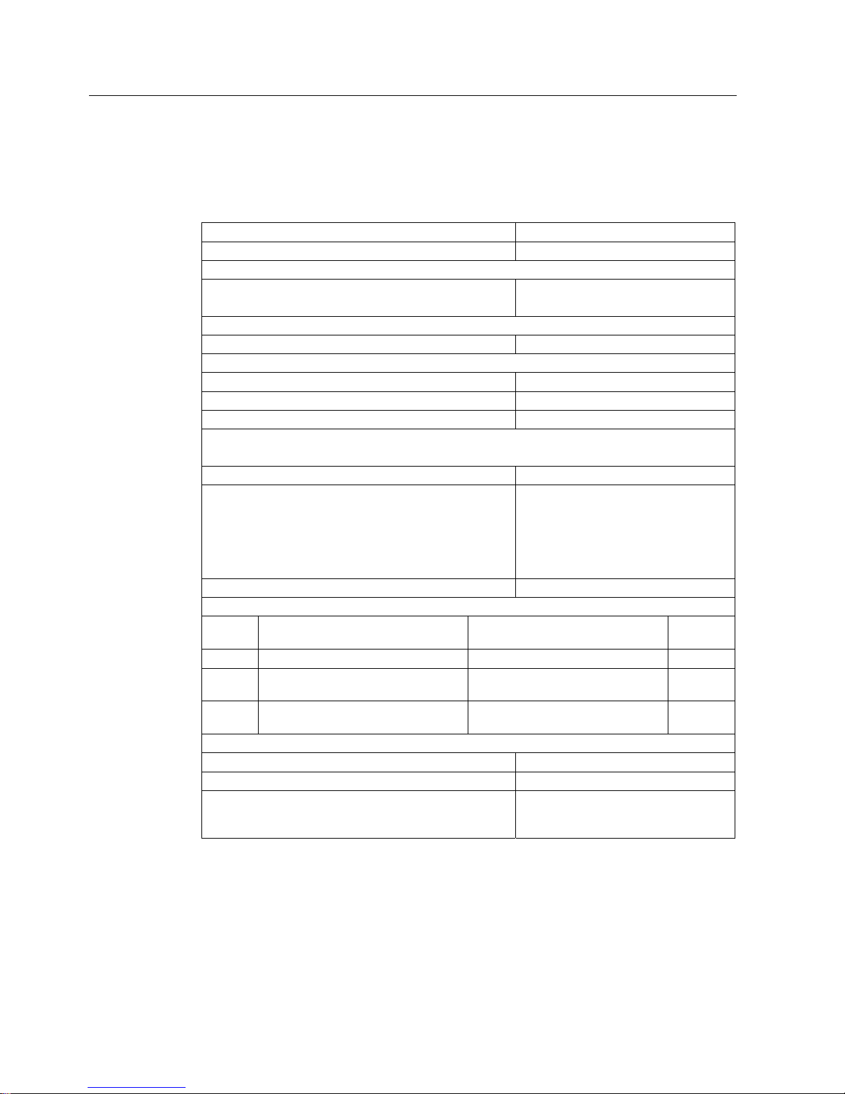
General technical specifications
Dimensions (W x H x D) 101 x 120 x 24 mm
Weight approx. 60 g
Supply voltage
P24V_EXT
Permitted voltage range
24V DC, NEC class 2
19.2 to 28.8 V
Power supply/Input/Input current
from load voltage L+ (no-load) max. 40 mA
Power consumption, power loss, potentials, isolation test
Power consumption from PCIe x1: 3.3 V / 12 V 240 mA
Power loss, typically 3.5 W
Isolation test voltage 500 VDC
Electromagnetic Compatibility
The G-IO device version meets the following requirements:
Field of application Industrial area
Emitted interference EN 61000-6-4:2007
This apparatus does not meet the
requirements of EN 61000-6-3:2007,
Generic standards - Emission standard
for residential, commercial and light-
industrial environments.
Noise immunity: EN 61000-6-2:2005
Components for the overvoltage protection
Cons.
no.
Cable for Component
1)
Item no.
1 Supply UN = 24V DC BLITZDUCTOR® VT, BVT AD 24 918 402
2 Inputs of digital modules UN = 24V DC DEHNconnect RK, DCO RK ME 24
(I
L
= 0.5 A)
919 921
3 Outputs of digital modules UN = 24V
DC
DEHNconnect RK, DCO RK D 5 24
(I
L
= 10.0 A)
919 986
Status, interrupts, diagnostics
Status display Orange LED per channel
Interrupts No
Diagnostic functions Yes; Messages in case of voltage
failure, overload, excess temperature of
outputs
1)
Components of the BLITZDUCTOR® XT series can be remotely monitored with the
appropriate accessories. For further information, refer to http://www.dehn.de. Components
can be ordered directly at: DEHN+SÖHNE GMBH+CO.KG., Hans-Dehn-Str. 1, D-92318
Neumarkt, Tel. +49 (0)9181-906-730
Page 47
Technical specifications
3.2 Technical specifications
SIMATIC PCIe DIO4
Compact Operating Instructions, 11/2011, A5E03493449-01
15
Digital inputs
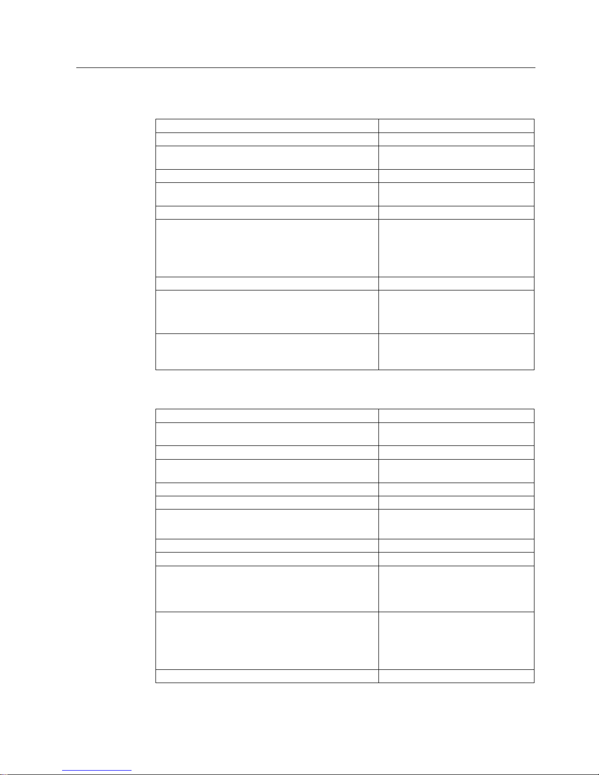
Number of inputs 4, controlled simultaneously
Input frequency Maximum 1 kHz
Required connector 8-pin, Weidmueller B2L 3.50/08/180 SN
BK BX; order no.: 1727650000
Cross section of connection cables at connector 0.08 mm2to 1.3 mm2
Inputs, interruptible Yes; on rising edge, falling edge or both
edges
Isolation between channels No
Input voltage
Rated value
For signal "0"
For signal "1"
24V DC
-3 to +5 V
+15 to 30 V
Input current for signal "1", typically 7 mA
Input delay at input voltage rated value
Adjustable filter times per input
Adjustable hysteresis per input
65.5 μs to 4 ms, increment 65.5 μs
1, 3, 5 or 7 samples
Status display Orange LED per channel
Control via logic; not directly connected
at input signal
Digital outputs
Number of outputs 4
Required connector 10-pin, Weidmueller B2L 3.50/10/180
SN BK BX; order no.: 1727660000
Cross section of connection cables at connector 0.08 mm2to 1.3 mm2
Outputs interruptible Yes; on rising edge, falling edge or both
edges
Integrated fuse Yes; 3.15 A
Isolation between channels No
Short-circuit protection
Response threshold, typically
Yes; electronic
0.6 A
Voltage induced on current interruption limited to L+ (-53 V)
Lamp load not permissible
Control of a digital input
Note: Because the output does not drive "0", the change
from "1" to "0" may take a long time with high-impedance
inputs.
Yes
A 100 K pull-down resistor is connected
at each output on the module.
Output current
For signal "1", rated value
For signal "1", minimum load current
For signal "0", residual current
0.5 A
5 mA
0.5 mA
Aggregate current of the outputs up to 50 °C max. 2 A
Page 48
Technical specifications
3.2 Technical specifications
SIMATIC PCIe DIO4
16 Compact Operating Instructions, 11/2011, A5E03493449-01
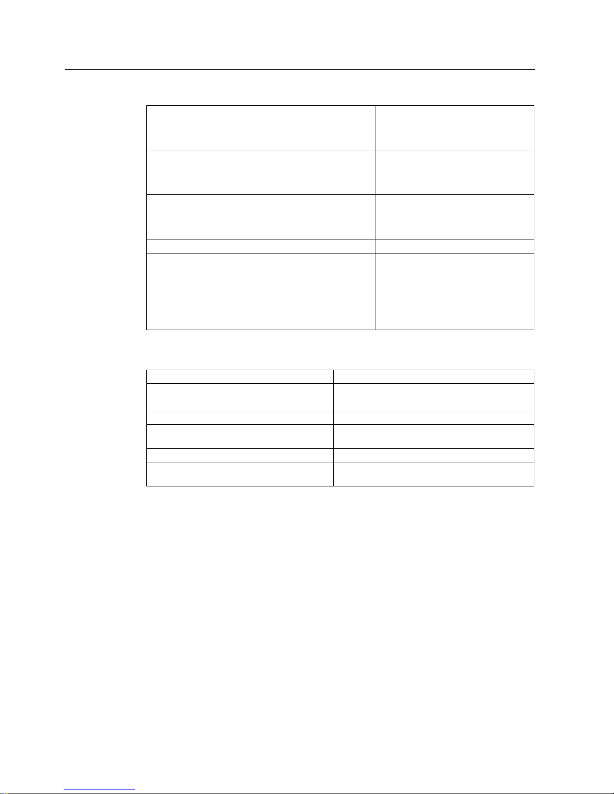
Output delay with ohmic load
"0" to "1"
"1" to "0"
max. 100 μs
max. 500 μs
Wiring two outputs in parallel
To increase performance
For redundant load control
No
Yes; only outputs of the same group
Switching frequency
For resistive load
For inductive load
max. 100 Hz
max. 0.5 Hz
Load resistance range 48 Ω to 4 kΩ
Outputs have a defined state
After a reset: Outputs are ZERO
(low).
With system standstill/crash:
Outputs remain in last set state and
can be reset with the device
watchdog.
Counters
Number of counters 8
Resolution 36 bit, 16 ns
Linking of inputs with counter Any
Linking of outputs with counter Any
Counter functions PWM, pulse width/frequency measurement,
counter up, down, delete, load, ...
Number of comparators per counter 1
Interrupt capability per counter Overflow, comparison less than/greater than/equal
to
Page 49

SIMATIC PCIe DIO4
Compact Operating Instructions, 11/2011, A5E03493449-01
17
Examples and register assignments
4
4.1 Initializing and enabling DIO
Enabling the DIO
To enable the DIO, abbreviation of digital IO module, proceed as follows:
1. Map the MMIO memory area from BAR0, hereafter referred to as BASE.
2. Check the version and the properties of the DIO from the VER register: BASE + 0x0000:
– Version = VER & 0xFF
– Revision = (VER >> 8) & 0xFF
– NumberOfInputs = (VER >> 16) & 0x1F
– NumberOfOutputs = (VER >> 21) & 0x1F
– NumberOfTimers = (VER >> 26) & 0x1F
3. Acquire the INUSE flag: InUse = (GSR & 1)
The INUSE flag prevents that several software components access the DIO at the same
time. Before a software accesses the DIO, the software must check if the module in
already in use by means of the INUSE flag. The result of the INUSE bit must be "0" when
the Global Status Register GSR is read for the first time. All other read accesses must
result in "1". The DIO is in use.
4. Set the GCR.EN. The DIO is enabled and the 24 V outputs are activated.
If you delete GCR.EN (0), all internal registers are reset.
The software now uses the DIO to run its program.
Disabling the DIO
Delete the GCR.EN. The internal registers are reset and the 24 V outputs are disabled.
Enabling the DIO
Write the INUSE flag GSR.INUSE; this step resets the INUSE flag.
Page 50

Examples and register assignments
4.2 Examples
SIMATIC PCIe DIO4
18 Compact Operating Instructions, 11/2011, A5E03493449-01
4.2 Examples
Example 1: Setting input filter for input 2
Input 2 is to be sampled with a period of 1 ms and a threshold value of 3. This results in the
following values:
● INP2C.FSRATE = 0xF
● INP2C.FTHRES = 0x1
● INP2C.ENF = 1
INP2C = 0x3D02
● Calculating the configuration address: INP2C = BASE + 0x200 + (2 * 8) = BASE + 0x210.
● Program INP2C with "0x3D02".
Example 2: Reading in input 2
The current input value (after optional filtering and inversion) is available in the INP register
(BASE + 0x100), bit 2.
Example 3: Setting output 1
Output 1 can be controlled with OUTP (BASE + 0x400), bit 1, if the output configuration for
output 1 has not been changed at address
OUTP1C (BASE + 0x500 + (1 * 8) = BASE + 0x508).
Example 4: Triggering interrupt at input 0 with rising edge
An interrupt is to be triggered with a rising edge at input 0. Enable the corresponding input
interrupt and the global interrupts as follows:
● Calculate the configuration address:
INP0C =BASE + 0x200 + (0 * 8) = BASE + 0x200
● Enable the input interrupt with rising edge:
Set INP0C.ENREI, INP0C |= 0x04
● Enable the input interrupts and global interrupts:
Set GCR.IIEN and GCR.IEN, GCR |= 0x06
Example 5: Treating an incoming interrupt
We recommend the following approach for incoming interrupts:
Determine the interrupt source by reading the GSR (GSR.IIF, GSR.OIF, GSR.CIF,
GSR.EIF):
● GSR.IIF: Evaluate INPIF, INPIFR and INPIFF and delete these interrupt flags through
writing (INPIF = INPIF deletes all input interrupts).
● GSR.OIF: Evaluate OUTPIF, OUTPIFR and OUTPIFF and delete these interrupt flags
through writing (OUTPIF = OUTPIF deletes all output interrupts).
Page 51

Examples and register assignments
4.2 Examples
SIMATIC PCIe DIO4
Compact Operating Instructions, 11/2011, A5E03493449-01
19
● GSR.CIF: Evaluate CxSR.IF. Evaluate CxSR.OIF, CxSR.CEIF, CxSR.CGIF and
CxSR.CSIF and delete these interrupts through writing.
● GSR.EIF: External error has occurred, e.g. missing output voltage or overload/short
circuit: Remedy the error and delete the GSR.EIF through writing.
Check GSR.IF to see if all interrupts have been processed.
Example 6: Measuring frequency at input 3
In this example we use counter 3 (C3) to measure the frequency of input 3. The rising edge
is used as time. Program C3 as follows:
Incrementing, clear + capture with rising edge of input 3.
● Calculating C3 address: C3BASE = BASE + 0x1000 + (3 * 0x100) = BASE + 0x1300.
● Programming event "Up": C3TR0 = 0x0100 (Source 0x01 = Always on)
● Programming event "Clear": C3TR2 = 0x2B08 (Source 0x2B = input 3, 0x08 = rising
edge)
● Programming event "Capture": C3TR4 = 0x2B08 (Source 0x2B = input 3, 0x08 = rising
edge)
● Enabling C3: C3CR.EN |= 1
The frequency is then calculated as follows: f
3
=1 / ( (C3CAPR +1) * 16 ns)
Example 7: Measuring pulse length at input 2
In this example we use counter 1 (C1) to measure the pulse length of the signal at input 2.
Program C1 as follows:
Incrementing, clear with rising edge, capture with falling edge of input 2.
● Calculating C1 address: C1BASE = BASE + 0x1000 + (1 * 0x100) = BASE + 0x1100.
● Programming event "Up": C1TR0 = 0x0100 (Source 0x01 = Always on)
● Programming event "Clear": C1TR2 = 0x2A08 (Source 0x2A = input 2, 0x08 = rising
edge)
● Programming event "Capture": C1TR4 = 0x2A0A (Source 0x2A = input 2, 0x0A = falling
edge)
● Enabling C1: C1CR.EN |= 1
The pulse length is then calculated as follows: t
pw2
= (C1CAPR + 1) * 16 ns
Page 52

Examples and register assignments
4.3 Registers
SIMATIC PCIe DIO4
20 Compact Operating Instructions, 11/2011, A5E03493449-01
4.3 Registers
The following abbreviations are used in the description of the registers:
● RO = Read Only. Read-only access.
● RW = Read, Write. Read and write access
● RWC = Read, Write/Clear. Read access. A write process deletes the corresponding bit.
Block Address Size
(bit)
Access Register Description
General BASE +
0x0000
32 RO VER Version: ID/Version/Capabilities
BASE +
0x0004
32 RW GCR General Control Register: Global Enable,
Global Interrupt Enable, ...
BASE +
0x0008
32 RWC GSR General Status Register: INUSE flag, Global
Interrupt flag, ...
Input BASE +
0x0100
32 RO INP Inputs 0-31 current value of the input signal
(after the input filter)
BASE +
0x0110
32 RWC INPIF Inputs 0-31 Interrupt flags, Input Interrupt
flags
BASE +
0x0120
32 RWC INPIFR Inputs 0-31 Interrupt flags (rising edge)
BASE +
0x0130
32 RWC INPIFF Inputs 0-31 Interrupt flags (falling edge)
BASE +
0x0200
64 RW INP0C Configuration of input 0: Filter, inversion,
interrupt, ..
BASE +
0x0208
64 RW INP1C Configuration of input 1: Filter, inversion,
interrupt, ..
BASE +
0x0210
64 RW INP2C Configuration of input 2: Filter, inversion,
interrupt, ..
BASE +
0x0218
64 RW INP3C Configuration of input 3: Filter, inversion,
interrupt, ..
... 64 RW INPnC Configuration of input n: Filter, inversion,
interrupt, ..
BASE +
0x02F8
64 RW INP31C Configuration of input 31: Filter, inversion,
interrupt, ..
Output BASE +
0x0400
32 RW OUTP Output 0-31 values
BASE +
0x0410
32 RWC OUTPIF Outputs 0-31 Interrupt flags
BASE +
0x0420
32 RWC OUTPIFR Outputs 0-31 Interrupt flags (rising edge)
BASE +
0x0430
32 RWC OUTPIFF Outputs 0-31 Interrupt flags (falling edge)
BASE +
0x0500
64 RW OUTP0C Configuration of output 0: Inversion, source,
...
BASE +
0x0508
64 RW OUTP1C Configuration of output 1: Inversion, source,
...
Page 53

Examples and register assignments
4.3 Registers
SIMATIC PCIe DIO4
Compact Operating Instructions, 11/2011, A5E03493449-01
21
Block Address Size
(bit)
Access Register Description
BASE +
0x0510
64 RW OUTP2C Configuration of output 2: Inversion, source,
...
BASE +
0x0518
64 RW OUTP3C Configuration of output 3: Inversion, source,
...
... 64 RW OUTPnC Configuration of output n: Inversion, source,
...
BASE +
0x05F8
64 RW OUTP31C Configuration of output 31: Inversion,
source, ...
Counter 0 BASE +
0x1000
32 RW C0CR Counter 0 Control Register
BASE +
0x1008
32 RW C0SR Counter 0 Status Register
BASE +
0x1010
56 RO C0VR Counter 0 Value Register
BASE +
0x1020
32 RW C0TR0 Counter 0 Trigger Register 0 ("Up")
BASE +
0x1028
32 RW C0TR1 Counter 0 Trigger Register 1 ("Down")
BASE +
0x1030
32 RW C0TR2 Counter 0 Trigger Register 2 ("Clear")
BASE +
0x1038
32 RW C0TR3 Counter 0 Trigger Register 3 ("Reload")
BASE +
0x1040
32 RW C0TR4 Counter 0 Trigger Register 4 ("Capture")
BASE +
0x1060
56 RW C0COMR Counter 0 Compare Register
BASE +
0x1070
56 RW C0RELR Counter 0 Reload Register
BASE +
0x1078
56 RW C0CAPR Counter 0 Capture Register
Counter 1 BASE +
0x1100
32 RW C1CR Counter 1 Control Register
BASE +
0x1108
32 RW C1SR Counter 1 Status Register
BASE +
0x1110
56 RO C1VR Counter 1 Value Register
BASE +
0x1120
32 RW C1TR0 Counter 1 Trigger Register 0 ("Up")
BASE +
0x1128
32 RW C1TR1 Counter 1 Trigger Register 1 ("Down")
BASE +
0x1130
32 RW C1TR2 Counter 1 Trigger Register 2 ("Clear")
BASE +
0x1138
32 RW C1TR3 Counter 1 Trigger Register 3 ("Reload")
BASE +
0x1140
32 RW C1TR4 Counter 1 Trigger Register 4 ("Capture")
Page 54
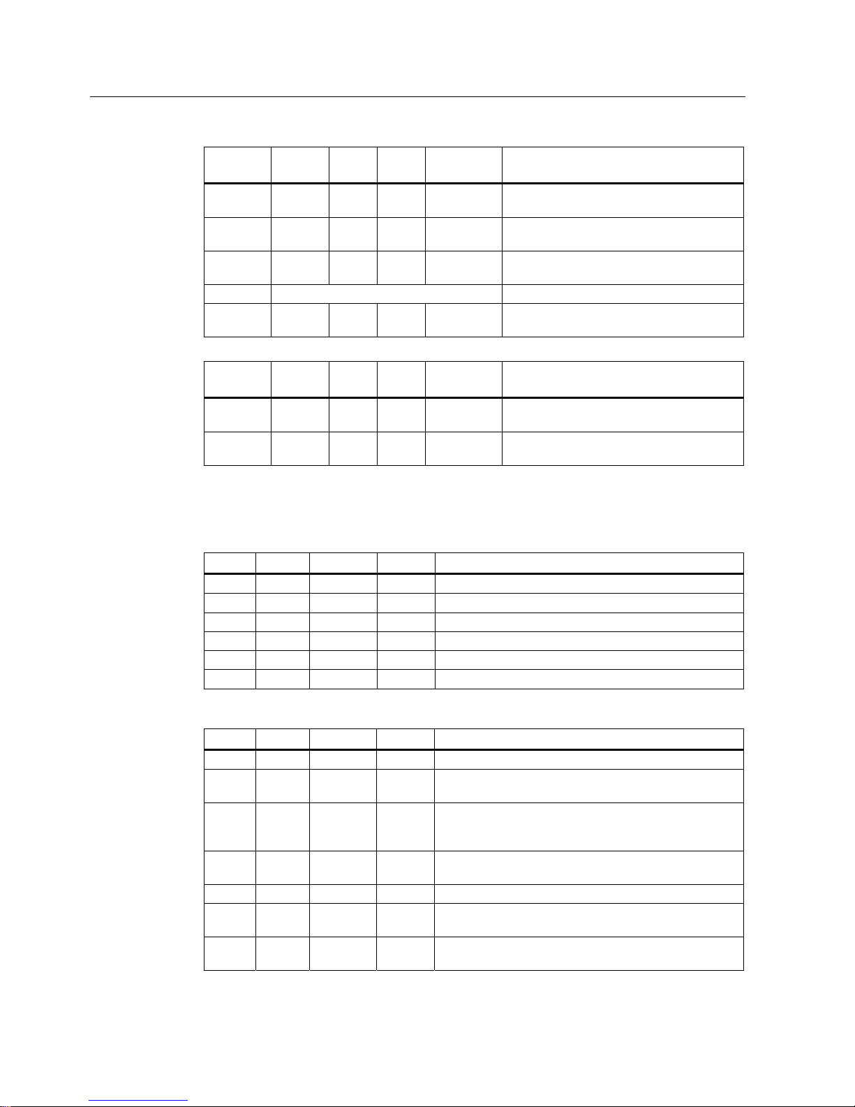
Examples and register assignments
4.3 Registers
SIMATIC PCIe DIO4
22 Compact Operating Instructions, 11/2011, A5E03493449-01
Block Address Size
(bit)
Access Register Description
BASE +
0x1160
56 RW C1COMR Counter 1 Compare Register
BASE +
0x1170
56 RW C1RELR Counter 1 Reload Register
BASE +
0x1178
56 RW C1CAPR Counter 1 Capture Register
Counter n The registers are repeated accordingly. See description above.
Counter 7 BASE +
0x1778
56 RW C7CAPR Counter 7 Capture Register
Block Address Size
(bit)
Access Register Description
BASE +
0x4040
32 RO PCIEIS PCIe core Interrupt Status Register
BASE +
0x4050
32 RW PCIEIE PCIe core Interrupt Enable Register
General Register
VER: Version (BASE + 0x0000)
Bit Access Name Default Description
31 RO 0 Reserved
30..26 RO NRCT 8 Number of counters/timers
25..21 RO NROP 4 Number of output signals
20..16 RO NRIP 4 Number of input signals
15..8 RO REV 00 Revision
7..0 RO VER 10 Version of the DIO interface (1.0)
GCR: General Control Register (BASE + 0x0004)
Bit Access Name Default Description
31..10 RO 0 Reserved
9 RW GATERST 0 If "1", the external reset is disabled (gated) so that the
DIO continues its operation even if the system restarts.
8 RW ENLOOP 0 Enables the loopback mode. If "1", all inputs are
internally connected with the output registers. The output
signals do not change their last value.
7 RW EIEN 0 Error interrupt enabled. If "1" and GSR.EIF = 1, GSR.IF
is set.
6..5 RO 0 Reserved
4 RW CIEN 0 Counter interrupt enabled. If "1" and GSR.CIF = 1,
GSR.IF is set.
3 RW OIEN 0 Output interrupt enabled. If "1" and GSR.OIF = 1, GSR.IF
is set.
Page 55
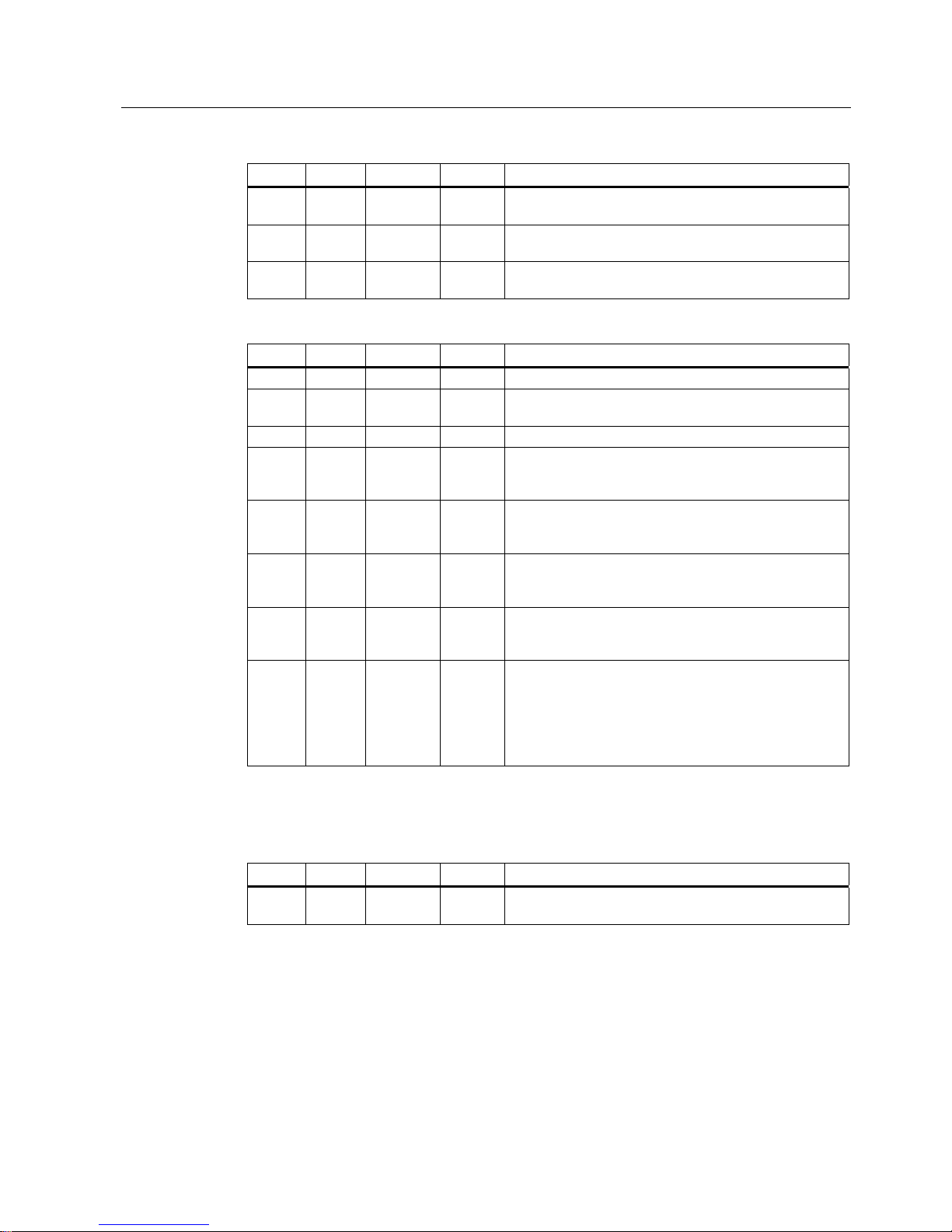
Examples and register assignments
4.3 Registers
SIMATIC PCIe DIO4
Compact Operating Instructions, 11/2011, A5E03493449-01
23
Bit Access Name Default Description
2 RW IIEN 0 Input interrupt enabled. If "1" and GSR.IIF = 1, GSR.IF is
set.
1 RW IEN 0 Global interrupt enabled. If "1", interrupts are enabled. If
STATUS.IF = 1, an interrupt is triggered.
0 RW EN 0 Global enable. Must be set to "1" for normal operation. If
set to "0", all internal registers are reset.
GSR: General Status Register (BASE + 0x0008)
Bit Access Name Default Description
31..8 RO 0 Reserved
7 RWC EIF 0 Error interrupt flag. If "1" an error has occurred. If the bit
is written with "1", the bit is reset.
6..5 RO 0 Reserved
4 RO CIF 0 Counter interrupt flag. If this flag was set, a counter has
triggered an interrupt. If all enabled counter interrupts are
deleted, the bit is reset.
3 RO OIF 0 Output interrupt flag. If this flag was set, an output has
triggered an interrupt. If all enabled output interrupts are
deleted, the bit is reset.
2 RO IIF 0 Input interrupt flag. If this flag was set, an input has
triggered an interrupt. If all enabled input interrupts are
deleted, the bit is reset.
1 RO IF 0 Interrupt flag. If EIF, CIF, OIF or IIF = 1, the flag is set. All
interrupts must be deleted to delete this bit. If the bit is
set and CONTROL.IEN =1, an interrupt is triggered.
0 RWC INUSE 0 The bit results in "0" at the first reading of the Global
Status Register GSR. All other read accesses must
result in "1". The DIO is in use.
Use the INUSE flag to prevent several drivers from
accessing the DIO. If the bit is written with "1", the bit is
reset.
Input Register
INP: Input register (BASE + 0x0100)
Bit Access Name Default Description
31..0 RO INx - Each bit reflects the corresponding input after filtering
and inversion.
Page 56
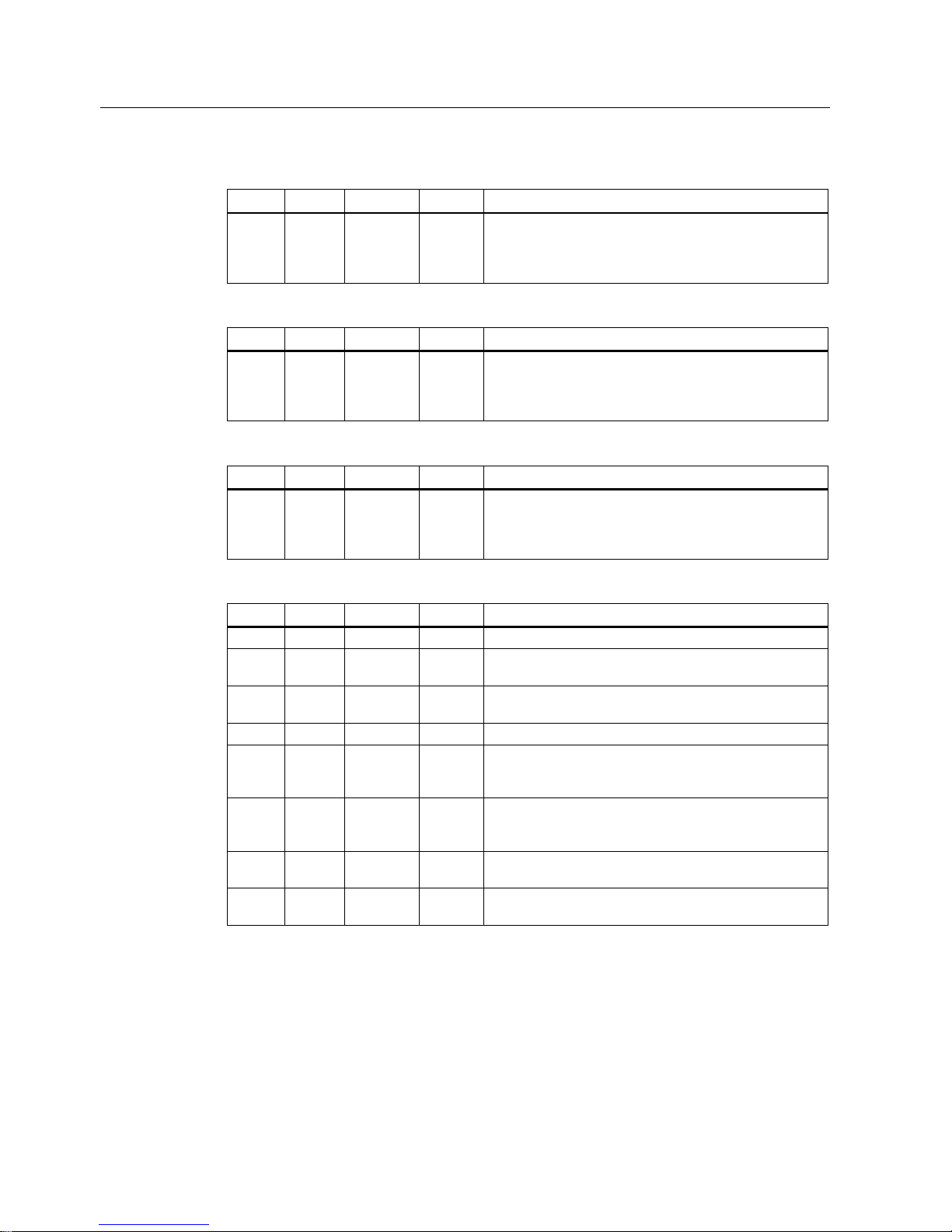
Examples and register assignments
4.3 Registers
SIMATIC PCIe DIO4
24 Compact Operating Instructions, 11/2011, A5E03493449-01
INPIF: Input interrupt flag register (BASE + 0x0110)
Bit Access Name Default Description
31..0 RWC IFx 0 Each bit reflects the interrupt state of the corresponding
input. If a bit is set, STATUS.IIF is set. If the bit is written
with "1", the bit is reset as well as the corresponding
IFRE/IFFE bits.
INPIFR: Input interrupt flag register, rising edge (BASE + 0x0120)
Bit Access Name Default Description
31..0 RWC IFREx 0 Each bit reflects the interrupt state of the rising edge of
the corresponding input. If a bit is set, STATUS.IIF is set.
If the bit is set, the corresponding INPUTIF.IF is set. If
the bit is written with "1", the bit is reset.
INPIFF: Input interrupt flag register, falling edge (BASE + 0x0130)
Bit Access Name Default Description
31..0 RWC IFFEx 0 Each bit reflects the interrupt state of the falling edge of
the corresponding input. If the bit is set, the
corresponding INPUTIF.IF is set. If the bit is written with
"1", the bit is reset.
INPxC: Input x configuration register (BASE + 0x0200 + (x*8))
Bit Access Name Default Description
63..16 RO 0 Reserved
15..10 RW FSRATE 0 Sample frequency input filter fs = 62.5 MHz / (FSRATE
<< 12).
9..8 RW FTHRES 0 Sample threshold input filter. 00: 1 sample, 01: 3
samples, 10: 5 samples, 11: 7 samples.
7..4 RO 0 Reserved
3 RW ENFEI 0 Enables an interrupt with a falling edge of the input
signal. If the bit is set and a falling edge is detected at
the input, the corresponding bit is set in INPIFF.IFFE.
2 RW ENREI 0 Enables an interrupt with a rising edge of the input
signal. If the bit is set and a rising edge is detected at the
input, the corresponding bit is set in INPIFR.IFRE.
1 RW ENF 0 Enables the input filter. If "1", the input is filtered with the
settings of FSRATE and FTHRES.
0 RW INV 0 If "1", the input signal is inverted before it is processed
further.
Page 57
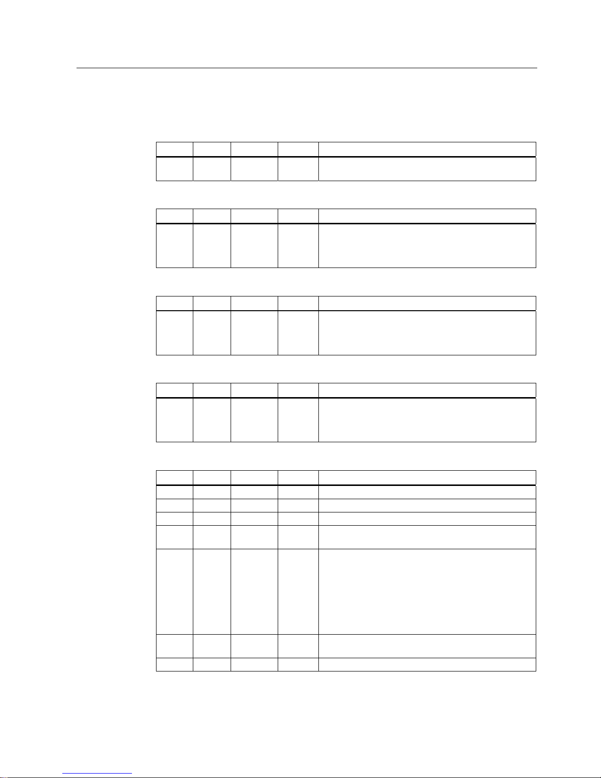
Examples and register assignments
4.3 Registers
SIMATIC PCIe DIO4
Compact Operating Instructions, 11/2011, A5E03493449-01
25
Output register
OUTP: Output register (BASE + 0x0400)
Bit Access Name Default Description
31..0 RW OUTx - Each bit reflects the corresponding output value in
default mode (OUTPxC.SSEL = 0).
OUTPIF: Output interrupt flag register (BASE + 0x0410)
Bit Access Name Default Description
31..0 RWC IFx 0 Each bit reflects the interrupt state of the corresponding
output. If a bit is set, STATUS.OIF is set. If the bit is
written with "1", the bit is reset as well as the
corresponding IFRE/IFFE bits.
OUTPIFR: Output interrupt flag register, rising edge (BASE + 0x0420)
Bit Access Name Default Description
31..0 RWC IFREx 0 Each bit reflects the interrupt state "Rising edge" of the
corresponding output. If a bit is set, STATUS.IIF is set. If
the bit is set, the corresponding OUTPIF.IF is set. If the
bit is written with "1", the bit is reset.
OUTPIFF: Output interrupt flag register, falling edge (BASE + 0x0430)
Bit Access Name Default Description
31..0 RWC IFFEx 0 Each bit reflects the interrupt state "Falling edge" of the
corresponding output. If the bit is set, the corresponding
OUTPIF.IF is set. If the bit is written with "1", the bit is
reset.
OUTP0C: Output x configuration register (BASE + 0x0500 + (x*8))
Bit Access Name Default Description
63..46 RO 0 Reserved
45..40 RW SSEL 0 Selection of output source, see "Output sources"
39..38 RO 0 Reserved
37..36 RW OMODE 0 Selection of output mode: 00: Normal, 01 = Changing
(1→0, 0→1)
35..33 RW DMODE 0 Selection of output detect mode:
000: High level
001: Low level
100: Rising edge only
101: Falling edge only
110: Rising and falling edge
32 RO OS 0 Status of the output selection. If "1", the output is
enabled.
31..4 RO 0 Reserved
Page 58
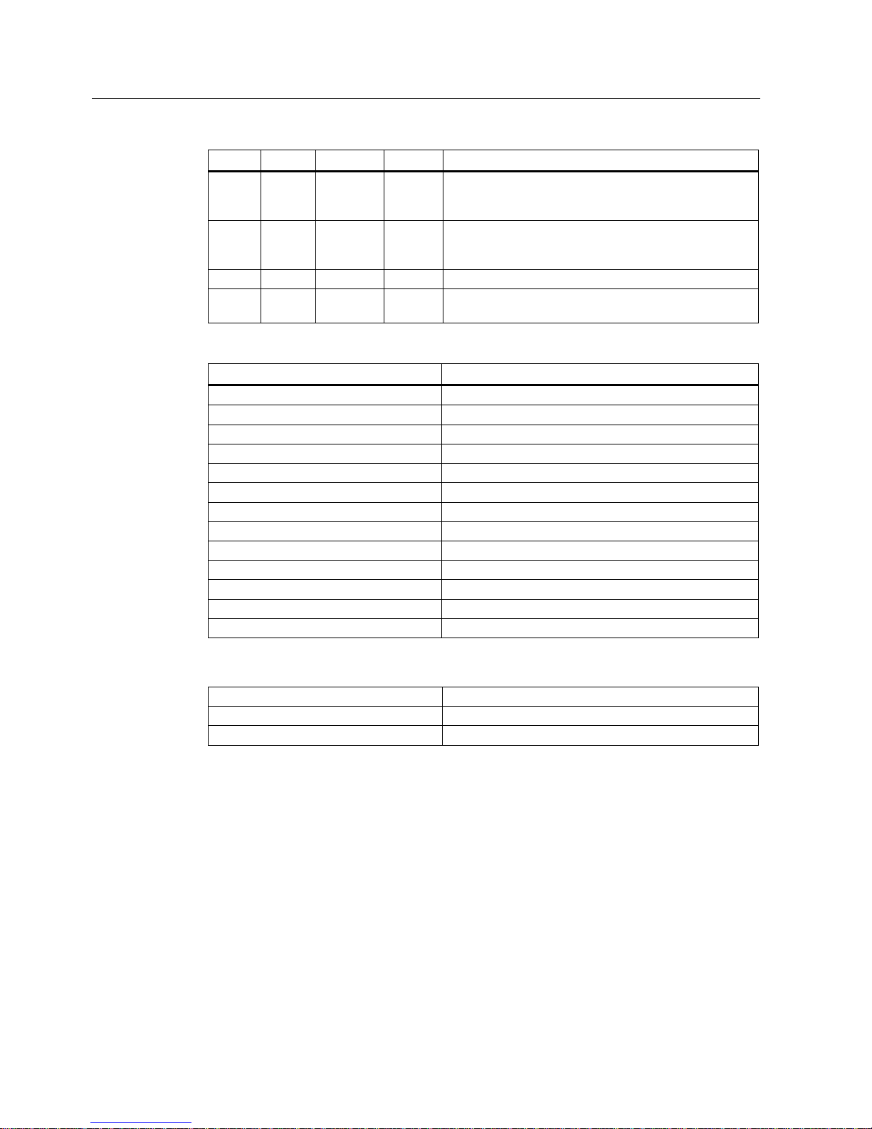
Examples and register assignments
4.3 Registers
SIMATIC PCIe DIO4
26 Compact Operating Instructions, 11/2011, A5E03493449-01
Bit Access Name Default Description
3 RW ENFEI 0 Enables an interrupt with a falling edge of the output
signal. If the bit is set and a falling edge is detected at
the output, the corresponding bit is set in OUTPIFF.IFFE.
2 RW ENREI 0 Enables an interrupt with a rising edge of the output
signal. If the bit is set and a rising edge is detected at the
output, the corresponding bit is set in OUTPIFR.IFRE.
1 RO 0 Reserved
0 RW INV 0 If "1", the output signal is inverted before it is processed
further.
Output sources
Values (decimal) Output signal
0 OUTPx
1 1
2 Reading DIO
3 Writing DIO
4 DIO Interrupt (GSR.IF)
5-7 Reserved
8/12/16/20/24/28/32/36 Counter x Overflow
9/13/17/21/25/29/33/37 Counter x Comparison "equal to" (CxSR.CE)
10/14/18/22/26/30/34/38 Counter x Comparison "greater than" (CxSR.CE)
11/15/19/23/27/31/35/39 Counter x Comparison "less than" (CxSR.CE)
40-43 Input 0-3 (INP 0..3)
44-47 Output 0-3 (OUTP 0..3)
48-63 Reserved
You should calculate the values for the index of input, output and counter according to the
following formula:
Counter x index Index = 8 + x*4
Input x index Index = 8 + VER.NRCT*4 + x
Output x index Index = 8 + VER.NRCT*4 + VER.NRIP + x
Page 59
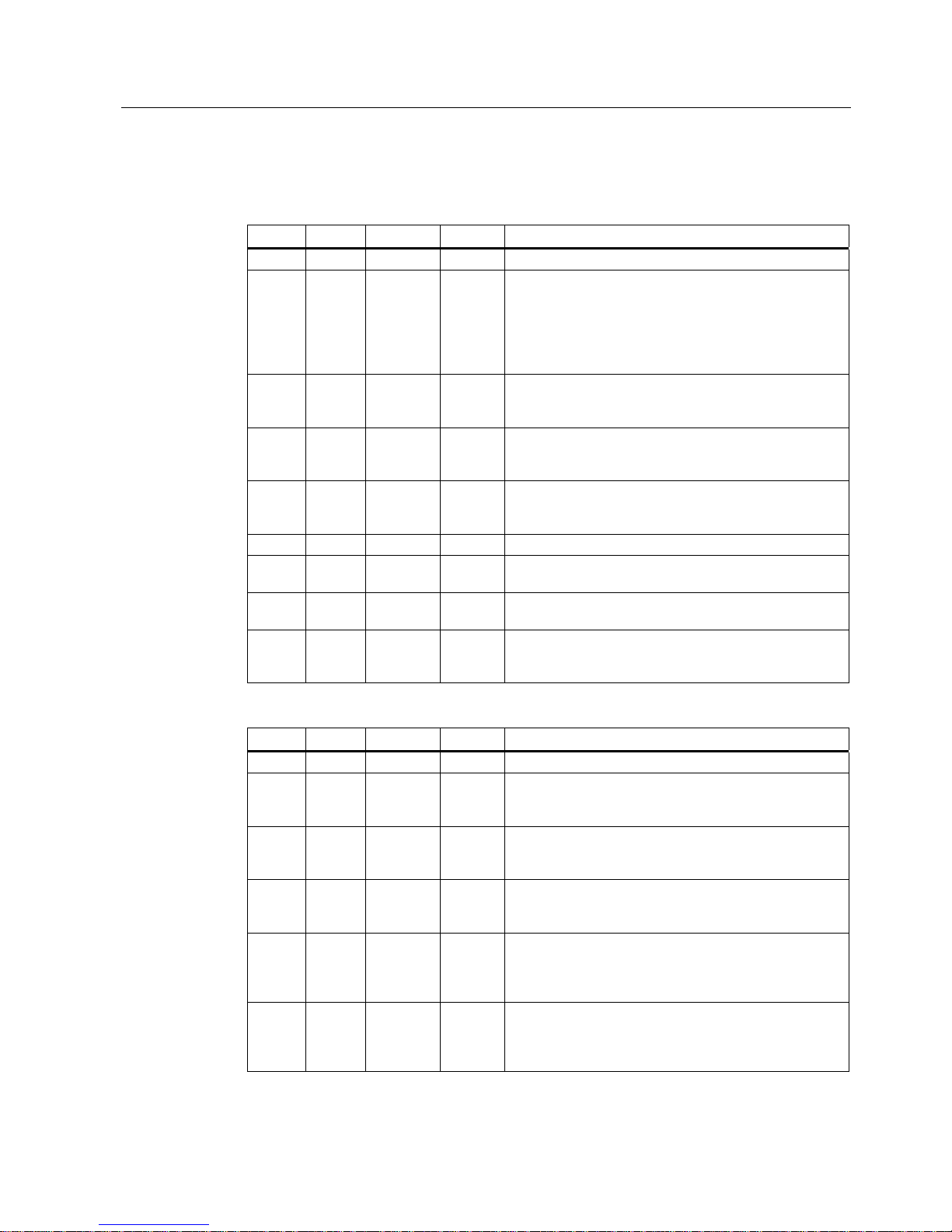
Examples and register assignments
4.3 Registers
SIMATIC PCIe DIO4
Compact Operating Instructions, 11/2011, A5E03493449-01
27
Counter Register
CxCR: Counter x Control Register (BASE + 0x1000 + (x*0x100))
Bit Access Name Default Description
31..9 RO 0 Reserved
8 RW CSEL 0 Selection of the Compare register (Compare).
0: Comparison of the Compare Register with the
Counter Register CVR
1: Comparison of the Compare Register with the
Capture Register CAPR
7 RW CSIEN 0 Enables an interrupt with the comparison result "less
than". If the bit is set to "1" and CxSR.CSIF = 1, CxSR.IF
is set.
6 RW CGIEN 0 Enables an interrupt with the comparison result "greater
than". If the bit is set to "1" and CxSR.CGIF = 1, CxSR.IF
is set.
5 RW CEIEN 0 Enables an interrupt with the comparison result "equal
to". If the bit is set to "1" and CxSR.CEIF = 1, CxSR.IF is
set.
4..3 RO 0 Reserved
2 RW OIEN 0 Enables an interrupt in case of counter overflow. If the bit
is set to "1" and CxSR.OIF = 1, CxSR.IF is set.
1 RW IEN 0 Enables a counter interrupt. If the bit is set to "1" and
CxSR.IF = 1, a counter interrupt is triggered.
0 RW EN 0 Enables the counter. If the bit is set to "1", the counter is
in operation. If "0", the counter is stopped and the
counter registers are reset.
CxSR: Counter x Status Register (BASE + 0x1008 + (x*0x100))
Bit Access Name Default Description
31..11 RO 0 Reserved
10 RO CS 0 Flag for comparison result "less than". If "1", the selected
compare register CxCR.CSEL is less than the compare
register.
9 RO CG 0 Flag for comparison result "greater than". If "1", the
selected compare register CxCR.CSEL is greater than
the compare register.
8 RO CE 0 Flag for comparison result "equal to". If "1", the selected
compare register CxCR.CSEL is equal to the compare
register.
7 RWC CSIF 0 Interrupt flag for comparison result "less than". If "1", an
interrupt is triggered with the comparison result "less
than": CxVR/CxCAPR < CxCOMR. If the bit is written
with "1", the bit is reset.
6 RWC CGIF 0 Interrupt flag for comparison result "greater than". If "1",
an interrupt is triggered with the comparison result
"greater than": CxVR/CxCAPR > CxCOMR. If the bit is
written with "1", the bit is reset.
Page 60
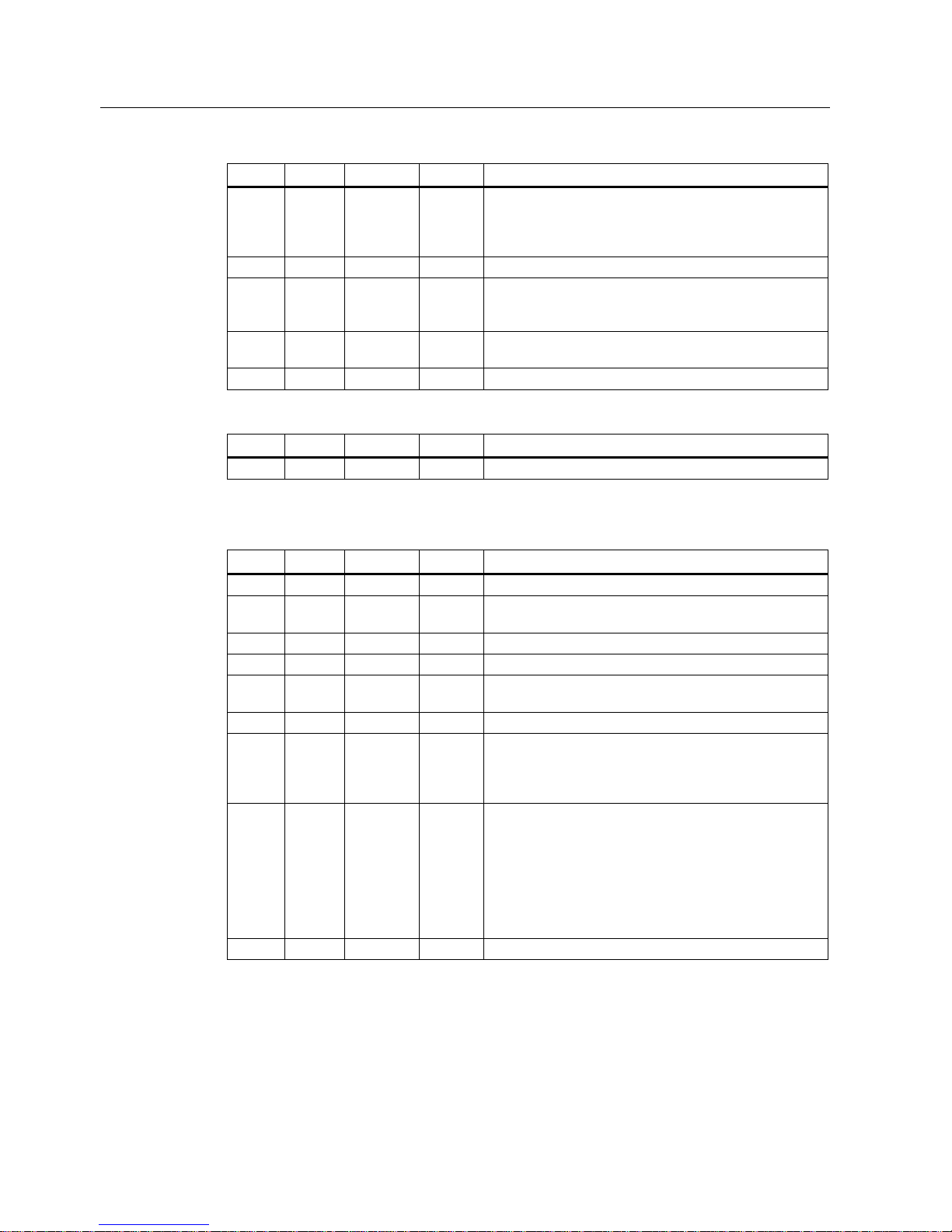
Examples and register assignments
4.3 Registers
SIMATIC PCIe DIO4
28 Compact Operating Instructions, 11/2011, A5E03493449-01
Bit Access Name Default Description
5 RWC CEIF 0 Interrupt flag for comparison result "equal to". If "1", an
interrupt is triggered with the comparison result "equal
to": CxVR/CxCAPR == CxCOMR. If the bit is written with
"1", the bit is reset.
4..3 RO 0 Reserved
2 RWC OIF 0 Interrupt flag for counter overflow. If "1", an interrupt is
triggered with a counter overflow. If the bit is written with
"1", the bit is reset.
1 RO IF 0 Interrupt flag for counter. If OIF, CEIF, CGIF or CSIF
were enabled and are active, the flag is set.
0 RO 0 Reserved
CxVR: Counter x Value Register (BASE + 0x1010 + (x*0x100))
Bit Access Name Default Description
35..0 RO 0 Current counter value
CxTR0: Counter x Trigger Register (BASE + 0x1020 + (x*0x100))
If the trigger is active, the counter is incremented.
Bit Access Name Default Description
31..24 RO 0 Reserved
23..16 RW PRE 0 Trigger pre-divider. Number of events until trigger is
enabled.
15..14 RO 0 Reserved
13..8 RW SSEL 0 Selection of trigger source, see "Output sources".
7 RW PEN 0 Pre-divider enabled. If "1", the trigger is pre-divided by
the value of PRE.
6 RO 0 Reserved
5..4 RW OMODE 0 Selection of trigger output mode:
00: Normal
01: Changing (1→0, 0→1)
3..1 RW DMODE 0 Selection of trigger detect mode:
000: High level
001: Low level
100: Rising edge only
101: Falling edge only
110: Rising and falling edge
0 RO TS 0 Trigger status. If "1", trigger is enabled.
Page 61

Examples and register assignments
4.3 Registers
SIMATIC PCIe DIO4
Compact Operating Instructions, 11/2011, A5E03493449-01
29
CxTR1: Counter 0 Trigger Register 1 (BASE + 0x1028 + (x*0x100))
If the trigger is enabled, the counter is decremented, see description CxTR0.
CxTR2: Counter 0 Trigger Register 2 (BASE + 0x1030 + (x*0x100))
If the trigger is enabled, the counter 0 is deleted, see description CxTR0.
CxTR3: Counter 0 Trigger Register 3 (BASE + 0x1038 + (x*0x100))
If the reload trigger is enabled, the counter is described with the value of CxRELR, see
description CxTR0.
CxTR4: Counter 0 Trigger Register 4 (BASE + 0x1040 + (x*0x100))
If the capture trigger is enabled, the current counter value of the counter is written to the
capture register CxCAPR, see description CxTR0.
Counter trigger sources
Value (decimal) Signal
0 0
1 1
2 Reading DIO
3 Writing DIO
4 DIO Interrupt (GSR.IF)
5-7 Reserved
8/12/16/20/24/28/32/36 Counter x Overflow
9/13/17/21/25/29/33/37 Counter x Comparison "equal to" (CxSR.CE)
10/14/18/22/26/30/34/38 Counter x Comparison "greater than" (CxSR.CE)
11/15/19/23/27/31/35/39 Counter x Comparison "less than" (CxSR.CE)
40-43 Input 0-3 (INP 0..3)
44-47 Output 0-3 (OUTP 0..3)
48-63 Reserved
You should calculate the values for the index of input, output and counter according to the
following formula:
Counter x index Index = 8 + x*4
Input x index Index = 8 + VER.NRCT*4 + x
Output x index Index = 8 + VER.NRCT*4 + VER.NRIP + x
CxCOMR: Counter x Compare Register (BASE + 0x1060 + (x*0x100))
Bit Access Name Default Description
35..0 RW CMP 0 Compare value
Page 62

Examples and register assignments
4.3 Registers
SIMATIC PCIe DIO4
30 Compact Operating Instructions, 11/2011, A5E03493449-01
If CxCR.CSEL = "0", the value of the register is compared with CxVR. If CxCR.CSEL = "1",
the value of the register is compared with CxCAPR. CxSR includes the comparison result:
CxSR.CE CxVR/CxCAPR is equal to CxCOMR.
CxSR.CG CxVR/CxCAPR is greater than CxCOMR.
CxSR.CS CxVR/CxCAPR is less than CxCOMR.
CxRELR: Counter x Reload Register (BASE + 0x1070 + (x*0x100))
If the reload trigger CxTR3 is enabled, the register is written to the counter register CxVR.
Bit Access Name Default Description
35..0 RW REL 0 Reload value
CxCAPR: Counter x Capture Register (BASE + 0x1078 + (x*0x100))
If the capture trigger CxTR4 is enabled, the current value of CxVR in saved in this register.
Bit Access Name Default Description
35..0 RW CAP 0 Capture value
PCIEIS: PCIe core Interrupt Status Register (BASE + 0x4040)
The register includes the interrupt status bit of the PCIe kernel.
Bit Access Name Default Description
31...8 RO Reserved
7 RO IA 0 Interrupt active: If this bit is set, the PCIe kernel signals
an interrupt to the system.
6...0 RO Reserved 0
PCIEIE: PCIe core Interrupt Enable Register (BASE + 0x4050)
The register includes the interrupt enable bit of the PCIe kernel. All bits with the exception of
bit 7 must be maintained and saved permanently.
Bit Access Name Default Description
31...8 RO Reserved
7 RW IE 0 Interrupt enable: If this bit is set, the PCIe kernel
forwards interrupts to the system. If this bit is not set, an
interrupt is not generated even if GCR.IEN is set.
6...0 RO Reserved 0
 Loading...