


ICs for Communications
Digital Answering Machine with Full Duplex Speakerphone
SAM EC
PSB 4860 Version 2.1
Data Sheet 10.97
DS 1

PSB 4860
Revision History: Current Version: 10.97
Previous Version: Preliminary Data Sheet 09.97
Page
(in previous
Version)
Page
(in new
Version)
Subjects (major changes since last revision)
Index added
Edition 10.97
This edition was realized using the software system FrameMaker
Published by Siemens AG,
HL TS
.
© Siemens AG 1997.
All Rights Reserved.
Attention please!
As far as patents or other rights of third parties are concerned, liability is only assumed for components, not for
applications, processes and c irc uit s imp lemented within components or as s em blies.
The information describe s the t yp e of co m ponent and shall not be considered as ass ured characteristics.
Terms of delivery and rights to ch ange design reserved.
For questions on technology, delivery and prices please contact the Semiconductor Group Offices in Germany or
the Siemens Companies and R epresentatives worldwide (see address list).
Due to technical requireme nt s com ponents may contain dangerous substances. For informatio n on t he t y pes in
question please contact yo ur nearest Siemens Office, Semiconductor Group.
Siemens AG is an approved CECC manufacturer.
Packing
Please use the recycling ope rat ors k now n t o y ou. W e ca n als o help you – get in touch with your nearest sa les
office. By agreement we will take packing material back, if it is sorted. You must bear the costs of transport.
For packing material that is returned to us unsorted or which we are not obliged to accept, we shall have to invoice
you for any costs incurred.
Components used in life-support devices or systems must be expressly authorized for such purpose!
Critical components
systems
1 A critical component is a component used in a life-support device or system whose failure can reasonably be
2 Life support devices or system s are int ended (a) to be implanted in the human body, or (b) to support and/or
2
with the express written approv al of the Semiconductor Group of Siemens AG.
expected to cause the failure of that life-support device or system, or to affect its safety or effectiveness of that
device or system.
maintain and sustain human life. If th ey fail, it is rea so nable to assume that the health of the us er m ay be endangered.
1
of the Semiconductor Group of Siemens AG, may only be used in life-s upport devices or

PSB 4860
Table of Contents Page
1Overview . . . . . . . . . . . . . . . . . . . . . . . . . . . . . . . . . . . . . . . . . . . . . . . . . .11
1.1 Features . . . . . . . . . . . . . . . . . . . . . . . . . . . . . . . . . . . . . . . . . . . . . . . . . .12
1.2 Pin Configuration . . . . . . . . . . . . . . . . . . . . . . . . . . . . . . . . . . . . . . . . . . . .13
1.3 Pin Definitions and Functions . . . . . . . . . . . . . . . . . . . . . . . . . . . . . . . . . .14
1.4 Logic Symbol . . . . . . . . . . . . . . . . . . . . . . . . . . . . . . . . . . . . . . . . . . . . . . .18
1.5 Functional Block Diagram . . . . . . . . . . . . . . . . . . . . . . . . . . . . . . . . . . . . .19
1.6 System Integration . . . . . . . . . . . . . . . . . . . . . . . . . . . . . . . . . . . . . . . . . . .19
1.6.1 Analog Featurephone with Digital Answering Machine . . . . . . . . . . . . . . .19
1.6.2 Featurephone with Digital Answering Machine for ISDN Terminal . . . . . .21
1.6.3 DECT Basestation with Integrated Digital Answering Machine . . . . . . . . .22
2 Functional Description . . . . . . . . . . . . . . . . . . . . . . . . . . . . . . . . . . . . . .23
2.1 Functional Units . . . . . . . . . . . . . . . . . . . . . . . . . . . . . . . . . . . . . . . . . . . . .27
2.1.1 Full Duplex Speakerphone . . . . . . . . . . . . . . . . . . . . . . . . . . . . . . . . . . . .27
2.1.2 Echo Cancellation . . . . . . . . . . . . . . . . . . . . . . . . . . . . . . . . . . . . . . . . . . .28
2.1.3 Echo Suppression . . . . . . . . . . . . . . . . . . . . . . . . . . . . . . . . . . . . . . . . . . .30
2.1.4 Line Echo Canceller . . . . . . . . . . . . . . . . . . . . . . . . . . . . . . . . . . . . . . . . .42
2.1.5 DTMF Detector . . . . . . . . . . . . . . . . . . . . . . . . . . . . . . . . . . . . . . . . . . . . .44
2.1.6 CNG Detector . . . . . . . . . . . . . . . . . . . . . . . . . . . . . . . . . . . . . . . . . . . . . .45
2.1.7 Alert Tone Detector . . . . . . . . . . . . . . . . . . . . . . . . . . . . . . . . . . . . . . . . . .46
2.1.8 CPT Detector . . . . . . . . . . . . . . . . . . . . . . . . . . . . . . . . . . . . . . . . . . . . . . .47
2.1.9 Caller ID Decoder . . . . . . . . . . . . . . . . . . . . . . . . . . . . . . . . . . . . . . . . . . .49
2.1.10 DTMF Generator . . . . . . . . . . . . . . . . . . . . . . . . . . . . . . . . . . . . . . . . . . . .51
2.1.11 Speech Coder . . . . . . . . . . . . . . . . . . . . . . . . . . . . . . . . . . . . . . . . . . . . . .52
2.1.12 Speech Decoder . . . . . . . . . . . . . . . . . . . . . . . . . . . . . . . . . . . . . . . . . . . .54
2.1.13 Analog Front End Interface . . . . . . . . . . . . . . . . . . . . . . . . . . . . . . . . . . . .55
2.1.14 Digital Interface . . . . . . . . . . . . . . . . . . . . . . . . . . . . . . . . . . . . . . . . . . . . .56
2.1.15 Universal Attenuator . . . . . . . . . . . . . . . . . . . . . . . . . . . . . . . . . . . . . . . . .58
2.1.16 Automatic Gain Control Unit . . . . . . . . . . . . . . . . . . . . . . . . . . . . . . . . . . .59
2.1.17 Equalizer . . . . . . . . . . . . . . . . . . . . . . . . . . . . . . . . . . . . . . . . . . . . . . . . . .61
2.2 Memory Management . . . . . . . . . . . . . . . . . . . . . . . . . . . . . . . . . . . . . . . .63
2.2.1 File Definition and Access . . . . . . . . . . . . . . . . . . . . . . . . . . . . . . . . . . . . .64
2.2.2 User Data Word . . . . . . . . . . . . . . . . . . . . . . . . . . . . . . . . . . . . . . . . . . . . .66
2.2.3 High Level Memory Management Commands . . . . . . . . . . . . . . . . . . . . .67
2.2.4 Low Level Memory Management Commands . . . . . . . . . . . . . . . . . . . . . .75
2.2.5 Execution Time . . . . . . . . . . . . . . . . . . . . . . . . . . . . . . . . . . . . . . . . . . . . .77
2.2.6 Special Notes on File Commands . . . . . . . . . . . . . . . . . . . . . . . . . . . . . . .78
2.3 Miscellaneous . . . . . . . . . . . . . . . . . . . . . . . . . . . . . . . . . . . . . . . . . . . . . .79
2.3.1 Real Time Clock . . . . . . . . . . . . . . . . . . . . . . . . . . . . . . . . . . . . . . . . . . . .79
2.3.2 SPS Control Register . . . . . . . . . . . . . . . . . . . . . . . . . . . . . . . . . . . . . . . .79
2.3.3 Reset and Power Down Mode . . . . . . . . . . . . . . . . . . . . . . . . . . . . . . . . . .79
2.3.4 Interrupt . . . . . . . . . . . . . . . . . . . . . . . . . . . . . . . . . . . . . . . . . . . . . . . . . . .80
2.3.5 Abort . . . . . . . . . . . . . . . . . . . . . . . . . . . . . . . . . . . . . . . . . . . . . . . . . . . . .81
Semiconductor Group 3 10.97

PSB 4860
Table of Contents Page
2.3.6 Revision Register . . . . . . . . . . . . . . . . . . . . . . . . . . . . . . . . . . . . . . . . . . .82
2.3.7 Hardware Configuration . . . . . . . . . . . . . . . . . . . . . . . . . . . . . . . . . . . . . . .82
2.3.8 Frame Synchronization . . . . . . . . . . . . . . . . . . . . . . . . . . . . . . . . . . . . . . .82
2.3.9 Clock Tracking . . . . . . . . . . . . . . . . . . . . . . . . . . . . . . . . . . . . . . . . . . . . . .83
2.3.10 Dependencies of Modules . . . . . . . . . . . . . . . . . . . . . . . . . . . . . . . . . . . . .83
2.4 Interfaces . . . . . . . . . . . . . . . . . . . . . . . . . . . . . . . . . . . . . . . . . . . . . . . . . .86
®
2.4.1 IOM
2.4.2 SSDI Interface . . . . . . . . . . . . . . . . . . . . . . . . . . . . . . . . . . . . . . . . . . . . . .90
2.4.3 Analog Front End Interface . . . . . . . . . . . . . . . . . . . . . . . . . . . . . . . . . . . .92
2.4.4 Serial Control Interface . . . . . . . . . . . . . . . . . . . . . . . . . . . . . . . . . . . . . . .94
2.4.5 Memory Interface . . . . . . . . . . . . . . . . . . . . . . . . . . . . . . . . . . . . . . . . . . . .98
2.4.6 Auxiliary Parallel Port . . . . . . . . . . . . . . . . . . . . . . . . . . . . . . . . . . . . . . .107
3 Detailed Register Description . . . . . . . . . . . . . . . . . . . . . . . . . . . . . . .109
3.1 Status Register . . . . . . . . . . . . . . . . . . . . . . . . . . . . . . . . . . . . . . . . . . . .109
3.2 Hardware Configuration Registers . . . . . . . . . . . . . . . . . . . . . . . . . . . . .111
3.3 Read/Write Registers . . . . . . . . . . . . . . . . . . . . . . . . . . . . . . . . . . . . . . .115
3.3.1 Register Table . . . . . . . . . . . . . . . . . . . . . . . . . . . . . . . . . . . . . . . . . . . . .115
3.3.2 Register Naming Conventions . . . . . . . . . . . . . . . . . . . . . . . . . . . . . . . . .117
-2 Interface . . . . . . . . . . . . . . . . . . . . . . . . . . . . . . . . . . . . . . . . . . . .86
4 Electrical Characteristics . . . . . . . . . . . . . . . . . . . . . . . . . . . . . . . . . . .225
4.1 Absolute Maximum Ratings . . . . . . . . . . . . . . . . . . . . . . . . . . . . . . . . . . .225
4.2 DC Characteristics . . . . . . . . . . . . . . . . . . . . . . . . . . . . . . . . . . . . . . . . . .225
4.3 AC Characteristics . . . . . . . . . . . . . . . . . . . . . . . . . . . . . . . . . . . . . . . . . .227
5 Package Outlines . . . . . . . . . . . . . . . . . . . . . . . . . . . . . . . . . . . . . . . . . .247
)
IOM®, IOM®-1, IOM®-2, SICOFI®, SICOFI®-2, SICOFI®-4, SICOFI®-4µC, SLICOFI®, ARCOFI
ARCOFI
SICAT
DigiTape
Semiconductor Group 4 10.97
®
-SP, EPIC®-1, EPIC®-S, ELIC®, IPAT®-2, ITAC®, ISAC®-S, ISAC®-S TE, ISAC®-P, ISAC®-P TE, IDEC®,
®
, OCTAT®-P, QUAT®-S are registered trademarks of S iem ens AG .
™
, MUSAC™-A, FALC™54, IWE™, SARE™, UTPT™, ASM™, ASP™ are trademarks of Siemens AG.
®
, ARCOFI®-BA,

PSB 4860
List of Figures Page
General
Figure 1: Pin Configuration of PSB 4860. . . . . . . . . . . . . . . . . . . . . . . . . . . . . . . . . 13
Figure 2: Logic Symbol of PSB 4860. . . . . . . . . . . . . . . . . . . . . . . . . . . . . . . . . . . . 18
Figure 3: Block Diagram of PSB 4860. . . . . . . . . . . . . . . . . . . . . . . . . . . . . . . . . . . 19
Figure 4: Analog Full Duplex Speakerphone with Digital Answering Machine . . . . 20
Figure 5: Featurephone with Answering Machine for ISDN Terminal . . . . . . . . . . . 21
Figure 6: DECT Basestation . . . . . . . . . . . . . . . . . . . . . . . . . . . . . . . . . . . . . . . . . . 22
Functional Units
Figure 7: Functional Units - Overview . . . . . . . . . . . . . . . . . . . . . . . . . . . . . . . . . . . 23
Figure 8: Functional Units - Recording a Phone Conversation . . . . . . . . . . . . . . . . 25
Figure 9: Functional Units - Simultaneous Internal and External Call . . . . . . . . . . . 26
Figure 10: Speakerphone - Signal Connections . . . . . . . . . . . . . . . . . . . . . . . . . . . . 27
Figure 11: Speakerphone - Block Diagram . . . . . . . . . . . . . . . . . . . . . . . . . . . . . . . . 27
Figure 12: Echo Cancellation Unit - Block Diagram. . . . . . . . . . . . . . . . . . . . . . . . . . 28
Figure 13: Echo Cancellation Unit - Typical Room Impulse Response . . . . . . . . . . . 29
Figure 14: Echo Suppression Unit - States of Operation. . . . . . . . . . . . . . . . . . . . . . 30
Figure 15: Echo Suppression Unit - Signal Flow Graph . . . . . . . . . . . . . . . . . . . . . . 31
Figure 16: Speech Detector - Signal Flow Graph . . . . . . . . . . . . . . . . . . . . . . . . . . . 32
Figure 17: Speech Comparator - Block Diagram. . . . . . . . . . . . . . . . . . . . . . . . . . . . 35
Figure 18: Speech Comparator - Interdependence of Parameters . . . . . . . . . . . . . . 36
Figure 19: Echo Suppression Unit - Automatic Gain Control. . . . . . . . . . . . . . . . . . . 39
Figure 20: Line Echo Cancellation Unit - Block Diagram. . . . . . . . . . . . . . . . . . . . . . 42
Figure 21: DTMF Detector - Block Diagram . . . . . . . . . . . . . . . . . . . . . . . . . . . . . . . 44
Figure 22: CNG Detector - Block Diagram . . . . . . . . . . . . . . . . . . . . . . . . . . . . . . . . 45
Figure 23: Alert Tone Detector - Block Diagram . . . . . . . . . . . . . . . . . . . . . . . . . . . . 46
Figure 24: CPT Detector - Block Diagram . . . . . . . . . . . . . . . . . . . . . . . . . . . . . . . . . 47
Figure 25: CPT Detector - Cooked Mode . . . . . . . . . . . . . . . . . . . . . . . . . . . . . . . . . 47
Figure 26: Caller ID Decoder - Block Diagram . . . . . . . . . . . . . . . . . . . . . . . . . . . . . 49
Figure 27: DTMF Generator - Block Diagram . . . . . . . . . . . . . . . . . . . . . . . . . . . . . . 51
Figure 28: Speech Coder - Block Diagram . . . . . . . . . . . . . . . . . . . . . . . . . . . . . . . . 52
Figure 29: Speech Decoder - Block Diagram . . . . . . . . . . . . . . . . . . . . . . . . . . . . . . 54
Figure 30: Analog Front End Interface - Block Diagram . . . . . . . . . . . . . . . . . . . . . . 55
Figure 31: Digital Interface - Block Diagram . . . . . . . . . . . . . . . . . . . . . . . . . . . . . . . 56
Figure 32: Universal Attenuator - Block Diagram . . . . . . . . . . . . . . . . . . . . . . . . . . . 58
Figure 33: Automatic Gain Control Unit - Block Diagram . . . . . . . . . . . . . . . . . . . . . 59
Figure 34: Equalizer - Block Diagram . . . . . . . . . . . . . . . . . . . . . . . . . . . . . . . . . . . . 61
Memory Management
Figure 35: Memory Management - Data Flow. . . . . . . . . . . . . . . . . . . . . . . . . . . . . . 63
Figure 36: Memory Management - Directory Structure . . . . . . . . . . . . . . . . . . . . . . . 63
Figure 37: Audio File Organization - Example. . . . . . . . . . . . . . . . . . . . . . . . . . . . . . 64
Figure 38: Binary File Organization - Example . . . . . . . . . . . . . . . . . . . . . . . . . . . . . 64
Semiconductor Group 5 10.97

PSB 4860
List of Figures Page
Figure 39: Phrase File Organization - Example. . . . . . . . . . . . . . . . . . . . . . . . . . . . . 65
Miscellaneous
Figure 40: Operation Modes - State Chart. . . . . . . . . . . . . . . . . . . . . . . . . . . . . . . . . 80
Interfaces
®-2
Figure 41: IOM
Figure 42: IOM
Figure 43: IOM
Figure 44: IOM
Figure 45: SSDI Interface - Transmitter Timing. . . . . . . . . . . . . . . . . . . . . . . . . . . . . 90
Figure 46: SSDI Interface - Active Pulse Selection . . . . . . . . . . . . . . . . . . . . . . . . . . 91
Figure 47: SSDI Interface - Receiver Timing. . . . . . . . . . . . . . . . . . . . . . . . . . . . . . . 91
Figure 48: Analog Front End Interface - Frame Structure . . . . . . . . . . . . . . . . . . . . . 92
Figure 49: Analog Front End Interface - Frame Start . . . . . . . . . . . . . . . . . . . . . . . . 93
Figure 50: Analog Front End Interface - Data Transfer . . . . . . . . . . . . . . . . . . . . . . . 93
Figure 51: Status Register Read Access. . . . . . . . . . . . . . . . . . . . . . . . . . . . . . . . . . 94
Figure 52: Data Read Access . . . . . . . . . . . . . . . . . . . . . . . . . . . . . . . . . . . . . . . . . . 95
Figure 53: Register Write Access . . . . . . . . . . . . . . . . . . . . . . . . . . . . . . . . . . . . . . . 95
Figure 54: Configuration Register Read Access . . . . . . . . . . . . . . . . . . . . . . . . . . . . 96
Figure 55: Configuration Register Write Access or Register Read Command . . . . . 96
Figure 56: ARAM/DRAM Interface - Connection Diagram. . . . . . . . . . . . . . . . . . . . . 99
Figure 57: ARAM/DRAM Interface - Read Cycle Timing. . . . . . . . . . . . . . . . . . . . . 100
Figure 58: ARAM/DRAM Interface - Write Cycle Timing . . . . . . . . . . . . . . . . . . . . . 101
Figure 59: ARAM/DRAM Interface - Refresh Cycle Timing. . . . . . . . . . . . . . . . . . . 101
Figure 60: EPROM Interface - Connection Diagram . . . . . . . . . . . . . . . . . . . . . . . . 102
Figure 61: EPROM Interface - Read Cycle Timing . . . . . . . . . . . . . . . . . . . . . . . . . 102
Figure 62: Flash Memory Interface - Connection Diagram . . . . . . . . . . . . . . . . . . . 103
Figure 63: Flash Memory Interface - Multiple Devices . . . . . . . . . . . . . . . . . . . . . . 104
Figure 64: Flash Memory Interface - Command Write. . . . . . . . . . . . . . . . . . . . . . . 105
Figure 65: Flash Memory Interface - Address Write . . . . . . . . . . . . . . . . . . . . . . . . 105
Figure 66: Flash Memory Interface - Data Write . . . . . . . . . . . . . . . . . . . . . . . . . . . 106
Figure 67: Flash Memory Interface - Data Read . . . . . . . . . . . . . . . . . . . . . . . . . . . 106
Figure 68: Auxiliary Parallel Port - Multiplex Mode . . . . . . . . . . . . . . . . . . . . . . . . . 108
Interface - Frame Structure . . . . . . . . . . . . . . . . . . . . . . . . . . . . . 86
®
-2 Interface - Frame Start. . . . . . . . . . . . . . . . . . . . . . . . . . . . . . . . . 87
®
-2 Interface - Single Clock Mode . . . . . . . . . . . . . . . . . . . . . . . . . . . 87
®
-2 Interface - Double Clock Mode . . . . . . . . . . . . . . . . . . . . . . . . . . 88
Electrical Characteristics
Figure 69: Input/Output Waveforms for AC-Tests . . . . . . . . . . . . . . . . . . . . . . . . . . 227
Timing Diagrams
Figure 70: Oscillator Circuits . . . . . . . . . . . . . . . . . . . . . . . . . . . . . . . . . . . . . . . . . . 231
®
Figure 71: SSDI/IOM
Figure 72: SSDI/IOM
-2 Interface - Bit Synchronization Timing . . . . . . . . . . . . . . . 232
®
-2 Interface - Frame Synchronization Timing . . . . . . . . . . . . 232
Figure 73: SSDI Interface - Strobe Timing. . . . . . . . . . . . . . . . . . . . . . . . . . . . . . . . 234
Semiconductor Group 6 10.97

PSB 4860
List of Figures Page
Figure 74: Serial Control Interface. . . . . . . . . . . . . . . . . . . . . . . . . . . . . . . . . . . . . . 235
Figure 75: Analog Front End Interface. . . . . . . . . . . . . . . . . . . . . . . . . . . . . . . . . . . 236
Figure 76: Memory Interface - DRAM Read Access . . . . . . . . . . . . . . . . . . . . . . . . 237
Figure 77: Memory Interface - DRAM Write Access . . . . . . . . . . . . . . . . . . . . . . . . 238
Figure 78: Memory Interface - DRAM Refresh Cycle . . . . . . . . . . . . . . . . . . . . . . . 239
Figure 79: Memory Interface - EPROM Read . . . . . . . . . . . . . . . . . . . . . . . . . . . . . 240
Figure 80: Memory Interface - Samsung Command Write . . . . . . . . . . . . . . . . . . . 241
Figure 81: Memory Interface - Samsung Address Write . . . . . . . . . . . . . . . . . . . . . 242
Figure 82: Memory Interface - Samsung Data Write . . . . . . . . . . . . . . . . . . . . . . . . 243
Figure 83: Memory Interface - Samsung Data Read. . . . . . . . . . . . . . . . . . . . . . . . 244
Figure 84: Auxiliary Parallel Port - Multiplex Mode . . . . . . . . . . . . . . . . . . . . . . . . . 245
Figure 85: Reset Timing . . . . . . . . . . . . . . . . . . . . . . . . . . . . . . . . . . . . . . . . . . . . . 246
Semiconductor Group 7 10.97

PSB 4860
List of Tables Page
General
Table 1: Pin Definitions and Functions. . . . . . . . . . . . . . . . . . . . . . . . . . . . . . . . . . .14
Functional Units
Table 2: Signal Summary . . . . . . . . . . . . . . . . . . . . . . . . . . . . . . . . . . . . . . . . . . . . .24
Table 3: Echo Cancellation Unit Registers. . . . . . . . . . . . . . . . . . . . . . . . . . . . . . . .28
Table 4: Speech Detector Parameters . . . . . . . . . . . . . . . . . . . . . . . . . . . . . . . . . . .34
Table 5: Speech Comparator Parameters . . . . . . . . . . . . . . . . . . . . . . . . . . . . . . . .37
Table 6: Attenuation Control Unit Parameters . . . . . . . . . . . . . . . . . . . . . . . . . . . . .38
Table 7: SPS Output Encoding. . . . . . . . . . . . . . . . . . . . . . . . . . . . . . . . . . . . . . . . .38
Table 8: Automatic Gain Control Parameters. . . . . . . . . . . . . . . . . . . . . . . . . . . . . .40
Table 9: Fixed Gain Parameters. . . . . . . . . . . . . . . . . . . . . . . . . . . . . . . . . . . . . . . .40
Table 10: Speakerphone Control Registers . . . . . . . . . . . . . . . . . . . . . . . . . . . . . . . .40
Table 11: Line Echo Cancellation Unit Registers. . . . . . . . . . . . . . . . . . . . . . . . . . . .43
Table 12: DTMF Detector Control Register . . . . . . . . . . . . . . . . . . . . . . . . . . . . . . . .44
Table 13: DTMF Detector Results . . . . . . . . . . . . . . . . . . . . . . . . . . . . . . . . . . . . . . .44
Table 14: DTMF Detector Parameters . . . . . . . . . . . . . . . . . . . . . . . . . . . . . . . . . . . .44
Table 15: CNG Detector Registers. . . . . . . . . . . . . . . . . . . . . . . . . . . . . . . . . . . . . . .45
Table 16: CNG Detector Result . . . . . . . . . . . . . . . . . . . . . . . . . . . . . . . . . . . . . . . . .45
Table 17: Alert Tone Detector Registers . . . . . . . . . . . . . . . . . . . . . . . . . . . . . . . . . .46
Table 18: Alert Tone Detector Results . . . . . . . . . . . . . . . . . . . . . . . . . . . . . . . . . . . .46
Table 19: CPT Detector Result. . . . . . . . . . . . . . . . . . . . . . . . . . . . . . . . . . . . . . . . . .48
Table 20: CPT Detector Registers . . . . . . . . . . . . . . . . . . . . . . . . . . . . . . . . . . . . . . .48
Table 21: Caller ID Decoder Modes . . . . . . . . . . . . . . . . . . . . . . . . . . . . . . . . . . . . . .49
Table 22: Caller ID Decoder Status . . . . . . . . . . . . . . . . . . . . . . . . . . . . . . . . . . . . . .49
Table 23: Caller ID Decoder Registers. . . . . . . . . . . . . . . . . . . . . . . . . . . . . . . . . . . .49
Table 24: DTMF Generator Registers . . . . . . . . . . . . . . . . . . . . . . . . . . . . . . . . . . . .51
Table 25: Speech Coder Status . . . . . . . . . . . . . . . . . . . . . . . . . . . . . . . . . . . . . . . . .52
Table 26: Speech Coder Registers . . . . . . . . . . . . . . . . . . . . . . . . . . . . . . . . . . . . . .53
Table 27: Speech Decoder Registers. . . . . . . . . . . . . . . . . . . . . . . . . . . . . . . . . . . . .54
Table 28: Analog Front End Interface Registers . . . . . . . . . . . . . . . . . . . . . . . . . . . .55
Table 29: Digital Interface Registers . . . . . . . . . . . . . . . . . . . . . . . . . . . . . . . . . . . . .56
Table 30: Universal Attenuator Registers. . . . . . . . . . . . . . . . . . . . . . . . . . . . . . . . . .58
Table 31: Automatic Gain Control Registers . . . . . . . . . . . . . . . . . . . . . . . . . . . . . . .59
Table 32: Equalizer Registers . . . . . . . . . . . . . . . . . . . . . . . . . . . . . . . . . . . . . . . . . .61
Memory Management - General
Table 33: Memory Management Registers . . . . . . . . . . . . . . . . . . . . . . . . . . . . . . . .65
Table 34: Memory Management Status . . . . . . . . . . . . . . . . . . . . . . . . . . . . . . . . . . .65
Table 35: Memory Management Parameters. . . . . . . . . . . . . . . . . . . . . . . . . . . . . . .66
Memory Management - Commands
Table 36: Initialize Memory Parameters. . . . . . . . . . . . . . . . . . . . . . . . . . . . . . . . . . .67
Semiconductor Group 8 10.97

PSB 4860
Table 37: Initialize Memory Results . . . . . . . . . . . . . . . . . . . . . . . . . . . . . . . . . . . . . .67
Table 38: Activate Memory Parameters. . . . . . . . . . . . . . . . . . . . . . . . . . . . . . . . . . .68
Table 39: Activate Memory Results . . . . . . . . . . . . . . . . . . . . . . . . . . . . . . . . . . . . . .68
Table 40: Activate Memory Result Interpretation. . . . . . . . . . . . . . . . . . . . . . . . . . . .68
Table 41: Open File Parameters . . . . . . . . . . . . . . . . . . . . . . . . . . . . . . . . . . . . . . . .69
Table 42: Open Next Free File Parameters . . . . . . . . . . . . . . . . . . . . . . . . . . . . . . . .69
Table 43: Open Next Free File Results . . . . . . . . . . . . . . . . . . . . . . . . . . . . . . . . . . .70
Table 44: Seek Parameters . . . . . . . . . . . . . . . . . . . . . . . . . . . . . . . . . . . . . . . . . . . .70
Table 45: Cut File Parameters . . . . . . . . . . . . . . . . . . . . . . . . . . . . . . . . . . . . . . . . . .71
Table 46: Compress File Parameters. . . . . . . . . . . . . . . . . . . . . . . . . . . . . . . . . . . . .71
Table 47: Memory Status Parameters . . . . . . . . . . . . . . . . . . . . . . . . . . . . . . . . . . . .72
Table 48: Memory Status Results . . . . . . . . . . . . . . . . . . . . . . . . . . . . . . . . . . . . . . .72
Table 49: Garbage Collection Parameters. . . . . . . . . . . . . . . . . . . . . . . . . . . . . . . . .72
Table 50: Access File Descriptor Parameters . . . . . . . . . . . . . . . . . . . . . . . . . . . . . .73
Table 51: Access File Descriptor Results. . . . . . . . . . . . . . . . . . . . . . . . . . . . . . . . . .73
Table 52: Read Data Parameters. . . . . . . . . . . . . . . . . . . . . . . . . . . . . . . . . . . . . . . .73
Table 53: Read Data Results . . . . . . . . . . . . . . . . . . . . . . . . . . . . . . . . . . . . . . . . . . .73
Table 54: Write Data Parameters. . . . . . . . . . . . . . . . . . . . . . . . . . . . . . . . . . . . . . . .74
Table 55: Set Address Parameters . . . . . . . . . . . . . . . . . . . . . . . . . . . . . . . . . . . . . .75
Table 56: DMA Read Parameters . . . . . . . . . . . . . . . . . . . . . . . . . . . . . . . . . . . . . . .75
Table 57: DMA Read Results. . . . . . . . . . . . . . . . . . . . . . . . . . . . . . . . . . . . . . . . . . .75
Table 58: DMA Write Parameters . . . . . . . . . . . . . . . . . . . . . . . . . . . . . . . . . . . . . . .76
Table 59: Block Erase Parameters. . . . . . . . . . . . . . . . . . . . . . . . . . . . . . . . . . . . . . .76
Table 60: Execution Times. . . . . . . . . . . . . . . . . . . . . . . . . . . . . . . . . . . . . . . . . . . . .77
Miscellaneous
Table 61: Real Time Clock Registers. . . . . . . . . . . . . . . . . . . . . . . . . . . . . . . . . . . . .79
Table 62: SPS Registers . . . . . . . . . . . . . . . . . . . . . . . . . . . . . . . . . . . . . . . . . . . . . .79
Table 63: Power Down Bit . . . . . . . . . . . . . . . . . . . . . . . . . . . . . . . . . . . . . . . . . . . . .80
Table 64: Interrupt Source Summary . . . . . . . . . . . . . . . . . . . . . . . . . . . . . . . . . . . . .81
Table 65: Hardware Configuration Checklist . . . . . . . . . . . . . . . . . . . . . . . . . . . . . . .82
Table 66: Frame Synchronization Selection. . . . . . . . . . . . . . . . . . . . . . . . . . . . . . . .82
Table 67: Dependencies of Modules . . . . . . . . . . . . . . . . . . . . . . . . . . . . . . . . . . . . .83
Table 68: File Command Classes . . . . . . . . . . . . . . . . . . . . . . . . . . . . . . . . . . . . . . .83
Table 69: Module Weights . . . . . . . . . . . . . . . . . . . . . . . . . . . . . . . . . . . . . . . . . . . . .84
Interfaces
®
Table 70: SSDI vs. IOM
®
Table 71: IOM
-2 Interface Registers. . . . . . . . . . . . . . . . . . . . . . . . . . . . . . . . . . . . .88
-2 Interface . . . . . . . . . . . . . . . . . . . . . . . . . . . . . . . . . . . . .86
Table 72: SSDI Interface Register . . . . . . . . . . . . . . . . . . . . . . . . . . . . . . . . . . . . . . .91
Table 73: Control of ALS Amplifier. . . . . . . . . . . . . . . . . . . . . . . . . . . . . . . . . . . . . . .92
Table 74: Analog Front End Interface Register . . . . . . . . . . . . . . . . . . . . . . . . . . . . .92
Table 75: Analog Front End Interface Clock Cycles. . . . . . . . . . . . . . . . . . . . . . . . . .93
Semiconductor Group 9 10.97

PSB 4860
Table 76: Command Words for Register Access . . . . . . . . . . . . . . . . . . . . . . . . . . . .97
Table 77: Address Field W for Configuration Register Write . . . . . . . . . . . . . . . . . . .97
Table 78: Address Field R for Configuration Register Read . . . . . . . . . . . . . . . . . . .97
Table 79: Supported Memory Configurations. . . . . . . . . . . . . . . . . . . . . . . . . . . . . . .98
Table 80: Address Line Usage (ARAM/DRAM Mode) . . . . . . . . . . . . . . . . . . . . . . .100
Table 81: Refresh Frequency Selection . . . . . . . . . . . . . . . . . . . . . . . . . . . . . . . . . .101
Table 82: Address Line Usage (Samsung Mode). . . . . . . . . . . . . . . . . . . . . . . . . . .103
Table 83: Flash Memory Command Summary. . . . . . . . . . . . . . . . . . . . . . . . . . . . .104
Table 84: Static Mode Registers . . . . . . . . . . . . . . . . . . . . . . . . . . . . . . . . . . . . . . .107
Table 85: Multiplex Mode Registers . . . . . . . . . . . . . . . . . . . . . . . . . . . . . . . . . . . . .107
Table 86: Signal Encoding . . . . . . . . . . . . . . . . . . . . . . . . . . . . . . . . . . . . . . . . . . . .117
Electrical Characteristics
Table 87: Status Register Update Timing. . . . . . . . . . . . . . . . . . . . . . . . . . . . . . . . .230
Semiconductor Group 10 10.97

PSB 4860
Overview
1Overview
General
General
Combined with an anal og front end th e PSB 4860 provide s a s olution for embe dde d or
stand alone answering ma chine applica tions. Together wi th a standard microcont roller
for analog telephones these two chi ps form the co re of a featurep hone with fu ll duplex
speakerphone and answering machine capabilities.
™
The chip features recording by DigiTape
Messages recorded with DigiTape
™
can be played back with variable speed without
pitch alteration. Messages recorded with a higher bitrate can be converted into
messages with a lower b itrate arbitrarily. Current m embers of DigiTape (TM) span the
range from 3.3 kbit/s to 10.3 kbit/s.
Furthermore the PSB 4860, V2.1 has a full duplex s peakerphone, a caller ID dec oder,
DTMF recognition and generation and call progress tone detection. The frequency
response of cheap m icro phones or lou dspeak ers can be correct ed by a programma ble
equalizer.
, a family of high performance algorithms.
Messages and user da ta can be stored in ARAM/DRAM or flash mem ory wh ich can be
directly connected to the PSB 4860. The PSB 4860 also supports a voice prompt
EPROM for fixed announcements.
®
The PSB 4860 provides an IOM
-2 compatible inte rface with t wo channels f or speech
data.
Alternatively to the IOM
®
-2 compatible interface the PSB 4 860 su pport s a si mple se rial
data interface (SSDI) with separate strobe sign als for each direction (linear PCM data,
one channel).
A separate interface is used for a glueless connection to the PSB 4851.
The chip is programmed by a simple four wire serial control interface and can inform the
microcontroller of new events by an interrupt sign al. For data retention the PSB 4860
supports a power down mode where only the real time clock and the memory refresh (in
case of ARAM/DRAM) are operational.
The PSB 4860 supports interface pins to +5 V levels.
Semiconductor Group 11 10.97
Digital Answering Machine with Full Duplex
PSB 4860
Speakerphone
SAM EC
Version 2.1 CMOS
1.1 Features
Digital Functions
• High performance recording by DigiTape
• Selectable compression rate (3.3 kbit/s, 10.3 kbit/s)
• Variable playback speed
• Support for ARAM or Flash Memory
• Optional voice prompt EPROM
• Full duplex speakerphone
• DTMF generation and detection
• Call progress tone detection
• Caller ID recognition
• Direct memory access
• Real time clock
• Equalizer
• Automatic gain control
• Automatic timestamp
• Auxiliary parallel port
• Ultra low power refresh mode
™
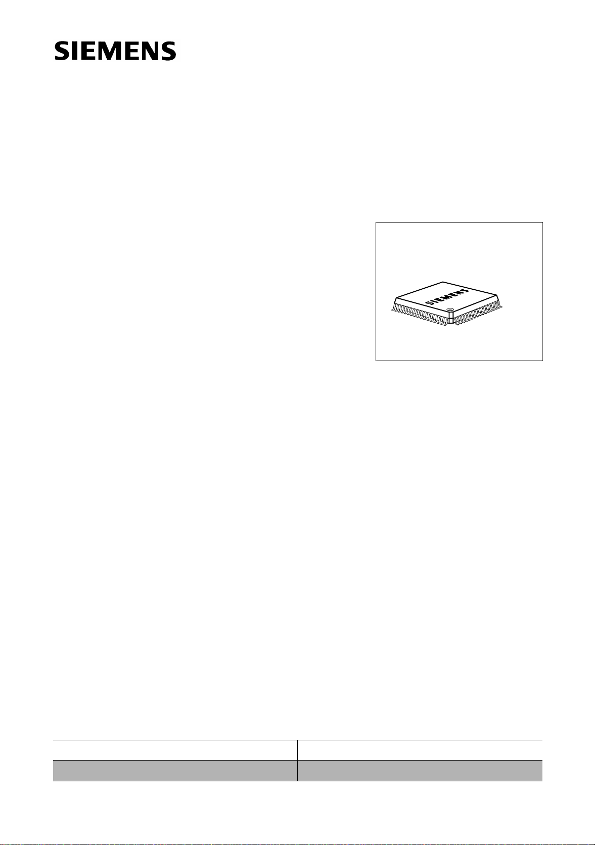
P-MQFP-80
General Features
®
• SSDI/IOM
-2 compatible interface
• Serial control interface for programming
Type Package
PSB 4860 P-MQFP-80
Semiconductor Group 12 10.97
1.2 Pin Configuration
(top view)
PSB 4860
Overview
V
MA
MA
MA
MA
V
MA
MA
MA
MA
V
MA
MA
MA
MA
RST
V
DD
V
SS
DD
10
11
V
SS
DD
12
13
14
15
V
SS
DDP
1MD2
3
MD
MD0V
DDP
VSSV
SS
VDDV
SS
MA3MA2MA1MA0MD7MD
RO
6
SS
MD5MD4MD
VDDV
4160 50
V
61
4
5
6
7
40
SS
V
DD
SPS
1
SPS
0
CAS1/FCS
CAS0/ALE
RAS
/FOE
/FCLE
8
9
70
SAM EC
PSB 4860
30
VPRD
W
/FWE
FRDY
V
SS
V
DD
DRST
DXST
DD/DR
DU/DX
DCL
FSC
V
SS
V
80
21
DD
110 20
DDA
V
XTAL1XTAL
2
SSA
V
OSC1OSC
2
V
DD
SS
V
INT
CLK
SDR
SDX
SCLK
CS
V
DD
SS
V
AFEFS
AFEDD
AFEDU
AFECLK
Figure 1 Pin Configuration of PSB 4860
Semiconductor Group 13 10.97

1.3 Pin Definitions and Functions
Table 1 Pin Definitions and Functions
PSB 4860
Overview
Pin No.
P-MQFP-80
41, 80
Symbol Dir. Reset Function
V
DDP
-- Power supply (5V %)
10±
Power supply for the interface.
7, 15, 21,
29, 39, 49,
V
DD
-- Power supply (3.0 V - 3.6 V)
Power supply for logic.
58, 61, 67,
73
1
V
DDA
-- Power supply (3.0 V - 3.6 V)
Power supply for clock generator.
4
V
SSA
-- Power supply (0 V)
Ground for clock generator.
9, 16, 22,
30, 40, 48,
V
SS
-- Power supply (0 V)
Ground for logic and interface.
57, 59, 60,
78, 66, 72
17 AFEFS O L Analog Frontend Frame Sync:
8 kHz frame synchronization signal for the
analog front end.
18 AFECLK O L Analog Frontend Clock:
Clock signal for the analog front end.
19 AFEDD O L Analog Frontend Data Downstream:
Data output to the analog frontend.
20 AFEDU I - Analog Frontend Data Upstream:
Data input from the analog frontend.
79 RST I - Reset:
Active high reset signal.
23 FSC I - Data Frame Synchronization:
8 kHz frame synchronization signal (IOM
SSDI mode).
24 DCL I - Data Clock:
Data Clock of the serial data interface.
®
-2 and
Semiconductor Group 14 10.97

Table 1 Pin Definitions and Functions
26 DD/DR I/ODI- IOM®-2 Compatible Mode:
Receive data from IOM
®
-2 controlling device.
SSDI Mode:
Receive data of the strobed serial data interface.
®
25 DU/DX I/OD
O/
OD
- IOM
Transmit data to IOM
SSDI Mode:
Transmit data of the strobed serial data
-2 Compatible Mode:
®
-2 controlling device.
interface.
27 DXST O L DX Strobe:
Strobe for DX in SSDI interface mode.
28 DRST I - DR Strobe:
Strobe for DR in SSDI interface mode.
PSB 4860
Overview
14 CS
I- Chip Select:
Select signal of the serial control interface (SCI).
11 SCLK I - Serial Clock:
Clock signal of the serial control interface (SCI).
13 SDR I - Serial Data Receive:
Data input of the serial control interface (SCI).
12 SDX O/
OD
10 INT
O/
OD
H Serial Data Transmit:
Data Output of the serial control interface (SCI).
H Interrupt
New status available.
Semiconductor Group 15 10.97

Table 1 Pin Definitions and Functions
52
53
54
55
62
63
64
65
68
69
70
71
74
75
76
77
MA
MA
MA
MA
MA
MA
MA
MA
MA
MA
MA
MA
MA
MA
MA
MA
0
1
2
3
4
5
6
7
8
9
10
11
12
13
14
15
I/O
I/O
I/O
I/O
I/O
I/O
I/O
I/O
I/O
I/O
I/O
I/O
I/O
I/O
I/O
I/O
1)
L
L
L
L
L
L
L
Memory Address 0-15:
Multiplexed address outputs for ARAM, DRAM
access.
Non-multiplexed address outputs for voice
prompt EPROM.
Auxiliary Parallel Port:
General purpose I/O.
L
L
L
L
L
L
L
L
L
PSB 4860
Overview
42
43
44
45
46
47
50
51
35
MD
MD
MD
MD
MD
MD
MD
MD
CAS
0
1
2
3
4
5
6
7
0
ALE
36
CAS
1
FCS
34 RAS
/
FOE
33 VPRD
FCLE
I/O
I/O
I/O
I/O
I/O
I/O
I/O
I/O
/
O
/
O
OH
/
OH
-
-
-
-
-
-
-
-
2)
H
2)
2)
Memory Data 0-7:
Memory (ARAM, DRAM, Flash Memory,
EPROM) data bus.
ARAM, DRAM:
Column address strobe for memory bank 0 or 1.
Flash Memory:
Address Latch Enable for address lines A
16-A23
Chip select signal for Flash Memory
ARAM, DRAM:
Row address strobe for both memory banks.
Flash Memory:
Output enable signal for Flash Memory.
ARAM, DRAM:
Read signal for voice prompt EPROM.
Flash Memory:
Command latch enable for Flash Memory.
.
Semiconductor Group 16 10.97

Table 1 Pin Definitions and Functions
32 W/FWE OH
2)
ARAM, DRAM:
Write signal for all memory banks.
Flash Memory:
Write signal for Flash Memory.
31 FRDY I - Flash Memory Ready
Input for Ready/Busy signal of Flash Memory
PSB 4860
Overview
5
6
OSC
OSC
1
2
I
O
Z
Auxiliary Oscillator:
Oscillator loop for 32.768 kHz crystal.
8CLKI-Alternative AFECLK Source
13,824 MHz
2
3
37
38
XTAL
XTAL
SPS
SPS
I
1
O
2
0
1
O
O
Z
L
L
Oscillator:
XTAL
XTAL
: External clock or input of oscillator loop.
1
: output of oscillator loop for crystal.
2
Multipurpose Outputs:
General purpose, speakerphone, address lines
or status
56 RO O - Reserved Output
Must be left open.
1)
These lines are driven low with 125 µA until the mode (address lines or auxi liary port ) is def ined.
2)
These lines are driven high with 70 µA during reset.
Semiconductor Group 17 10.97
1.4 Logic Symbol
1
PSB 4860
Overview
PSB
RST
AFECLK
AFEFS
AFEDD
AFEDU
V
DD
V
DDA
V
SS
MA0-MA15MD0-MD
OSC
CLK
PSB 4860
7
CAS0/
ALE
CAS1/
FCS
Memory
1
OSC
XTAL1XTAL
2
RAS/ VPRD/
FOE
W/
FWE
2
FCLE
DU/DX
DD/DR
DCL
FSC
DXST
DRST
SDX
SDR
SCLK
FRDY
IOM®-2
SSDI4851
INT
SCI
CS
Figure 2 Logic Symbol of PSB 4860
Semiconductor Group 18 10.97
1.5 Functional Block Diagram
PSB 4860
Overview
AFECLK
AFEFS
AFEDD
AFEDU
RST
Analog
Front End
Interface
1
OSC
XTAL1XTAL
2
OSC
Reset and Timing Unit
DSP
Memory Interface
2
DRST
DXST
Data
Interface
Control
Interface
DU/DX
DD/DR
DCL
FSC
INT
SDX
SDR
SCLK
CS
FRDY
MA
-MA15MD0-MD7CAS0/
0
ALE
CAS1/
FCS
RAS/VPRD/
FOE
W/
FWE
FCLE
Figure 3 Block Diagram of PSB 4860
1.6 System Integration
The PSB 4860 combined with an analo g fron t end (PSB 4 851 ) can be used in a variety
of applications. This combination offers outstanding features like full duplex
speakerphone and emergenc y operation. Some applicat ions are given in the followin g
sections.
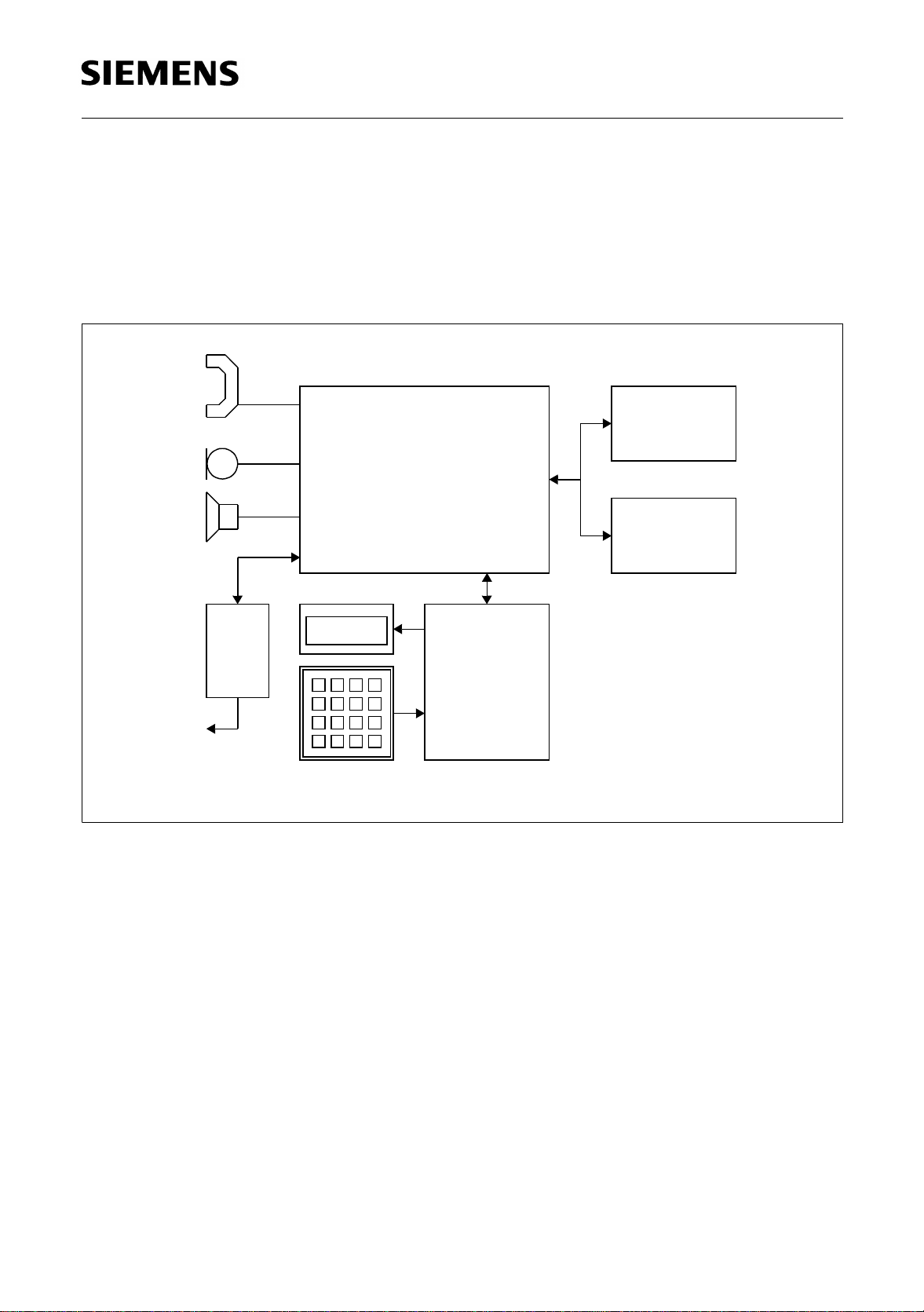
1.6.1 Analog Featurephone with Digital Answering Machine
Figure 4 shows an example of an analog telephone system. The telephone can operate
during power failure by line powering. In this case only the handset and ringer circuit are
active. All other parts of the chipset are shut down leaving enough power for the external
microcontroller to perform basic tasks like keyboard monitoring.
Semiconductor Group 19 10.97
PSB 4860
Overview
For answering machine operation the voice data is stored in ARAM or Flash Memory
devices. In addition, voice pro mpts can be played back from an optional vo ice prompt
EPROM. If flash memory is used the func tionality of the voice prompt EPROM c an be
realized by the flash memory devices. The microcontroller can use the memory attached
to the PSB 4860/PSB 4851 to store and retrieve binary data.
ARAM
Flash Memory
PSB 4860
PSB 4851
Voice Prompt
EPROM
077-3445
tip/
ring
line
Microcontroller
Figure 4 Analog Full Duplex Speakerphone with Digital Answering Machine
Semiconductor Group 20 10.97
PSB 4860
Overview
1.6.2 Featurephone with Digital Answering Machine for ISDN Terminal
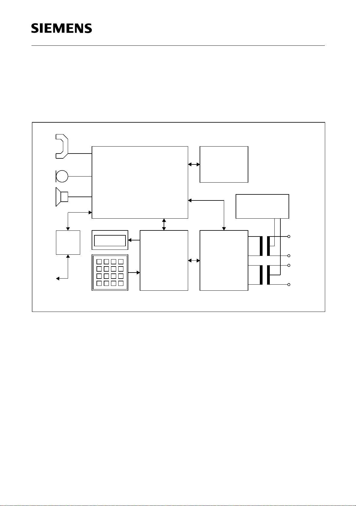
Figure 5 shows an ISDN featureph one that takes full advantage of two simu ltaneous
connections. In this a pplication o ne channel o f the PSB 4851 interfa ces to the hands et
and speakerphone while the other provides an interface for an externa l analog device
(e.g. FAX machine).
Flash Memory
PSB 4860
PSB 4851
IOM®-2
Power Controller
PSB 2120/1
SCI
SLIC
POTS
077-3445
Microcontroller
PSB 2186
®
-S TE
ISAC
S
-BUS
0
Figure 5 Featurephone with Answering Machine for ISDN Terminal
In addition, the two chann els of the PSB 485 1 ca n be use d for holdi ng two c on nec tion s
simultaneously. O ne connection can be switch ed to the handset and the other to the
speakerphone box. Local three party conferences are also possible.
Semiconductor Group 21 10.97
PSB 4860
Overview
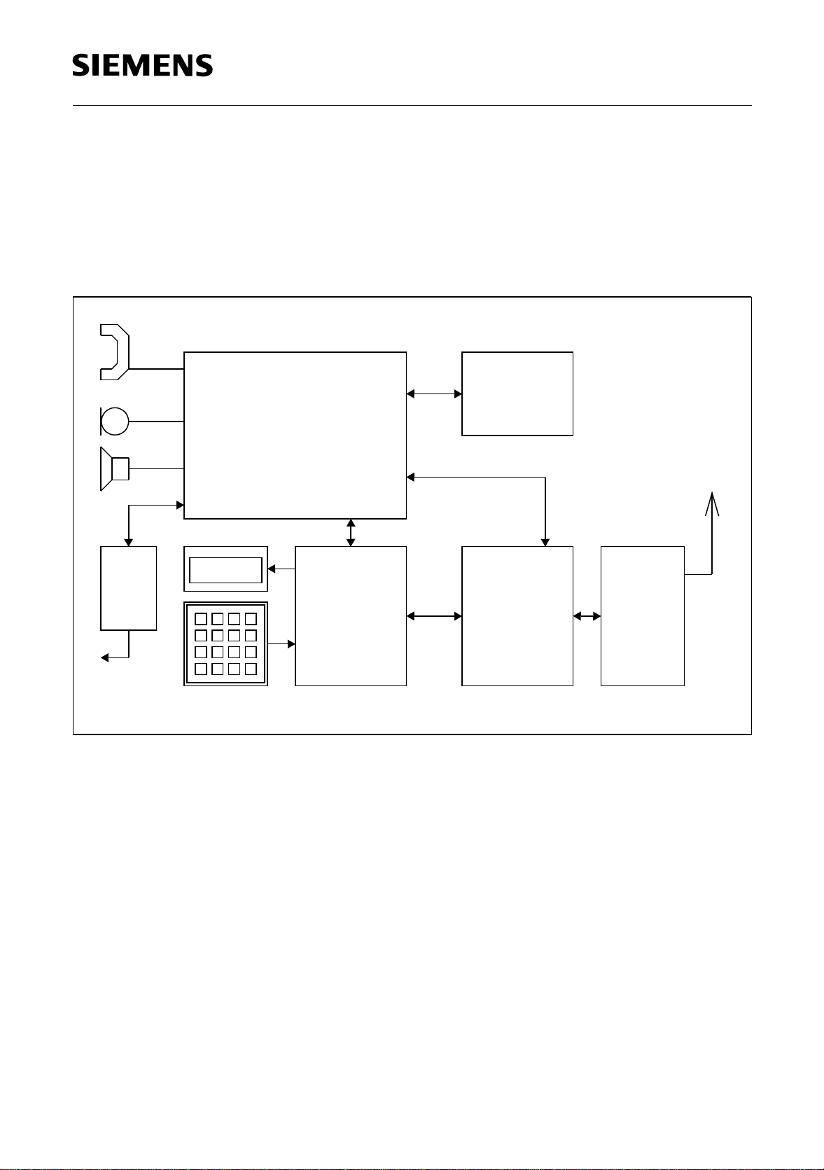
1.6.3 DECT Basestation with Integrated Digital Answering Machine
Figure 6 shows a DECT basestation based on the PSB 4860/PSB 4851 chi pset. In this
application it is possible to service both an external call and an internal call at the same
time. For programming the serial control interface (SCI) is used while voice data is
®
transferred via the strobed serial data interface (SSDI/IOM
Flash Memory
-2).
PSB 4860
PSB 4851
SSDI/IOM®-2
Antenna
077-3445
tip/
ring
Microcontroller
line
Figure 6 DECT Basestation
SCI
Burstmode
Controller
DECT
HF
Semiconductor Group 22 10.97
PSB 4860
Functional Description
2 Functional Description
Functional Units
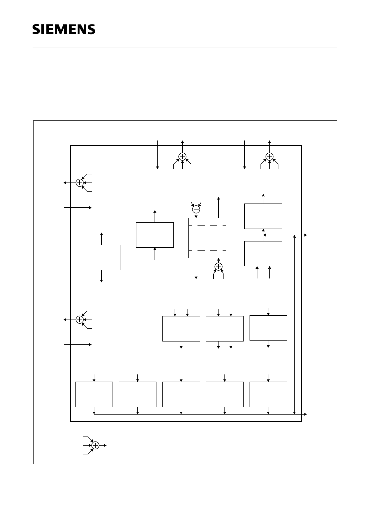
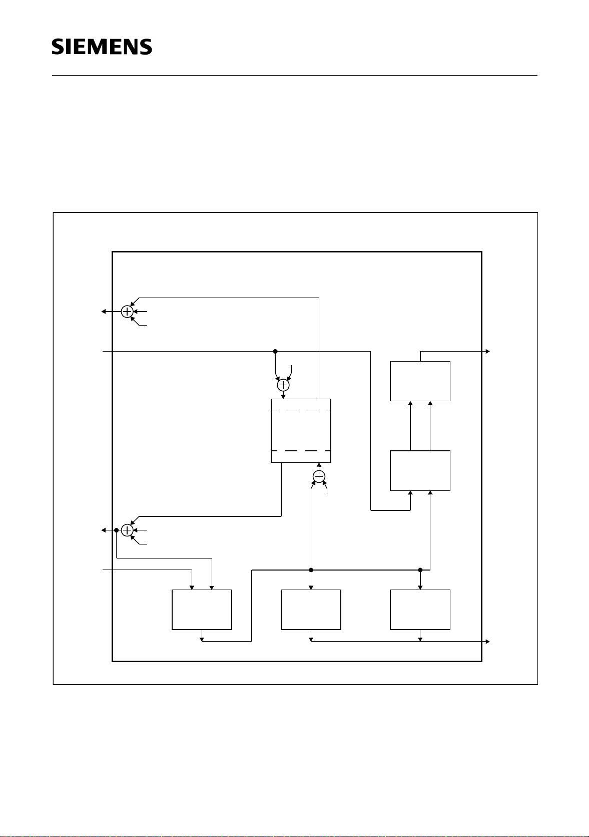
Functional Units
The PSB 4860 contains several functional units that can be combined wit h almost no
restrictions to perform a given task. Figure 7 gives an overview of the important
functional units.
®
SSDI/IOM
-2 IOM®-2
Channel 2Channel 1
loud-
speaker
microphone
line
out
line
in
S
4
S
2
I
1
I
2
I
3
S
3
S
9
DTMF
Generator
S
10
I
1
I
2
I
3
S
1
S
5
S
14
Universal
Attenuator
I
1
S
6
I1I2I
I1I
I1I
2
Line Echo
Canceller
S
15
3
S
2
acoustic side
Speaker-
phone
line side
S
12
I3I
S
11
4
I1I
AGC
16
S
8
S
I1I2I
7
S
3
13
Speech
Decoder
Memory
Speech
Coder
I1I
2
I
2
1
Equalizer
S
17
S
18
I
1
CNG
Detector
I
1
Alert Tone
Detector
I
1
CPT
Detector
I
1
CID
Decoder
I
1
DTMF
Detector
SCI
signal summation: s igna l sou rc es:
I
1
I
2
I
3
S
,...,S
1
18
Figure 7 Functional Units - Overview
Semiconductor Group 23 10.97

PSB 4860
Functional Description
Each unit has one or more signa l inputs (denoted by I). Most units have at least one
signal output (denoted by S). Any input I can be co nnected to any signal output S. In
addition to the sign als shown in figure 7 there is also the signal S
useful at signal summation points. Table 2 lists the available signals within the PSB 4860
according to their reference points.
Table 2 Signal Summary
Signal Description
(silence), which is
0
S
S
S
S
S
S
S
S
S
S
S
S
S
S
S
0
1
2
3
4
5
6
7
8
9
10
11
12
13
14
Silence
Analog line input (channel 1 of PSB 4851 interface)
Analog line output (channel 1 of PSB 4851 interface)
Microphone input (channel 2 of PSB 4851 interface)
Loudspeaker/Handset output (channel 2 of PSB 4851 interface)
Serial interface input, channel 1
Serial interface output, channel 1
Serial interface input, channel 2
Serial interface output, channel 2
DTMF generator output
DTMF generator auxiliary output
Speakerphone output (acoustic side)
Speakerphone output (line side)
Speech decoder output
Universal attenuator output
S
15
S
16
S
17
S
18
Semiconductor Group 24 10.97
Line echo canceller output
Automatic gain control output (after gain stage)
Automatic gain control output (before gain stage)
Equalizer output
PSB 4860
Functional Description
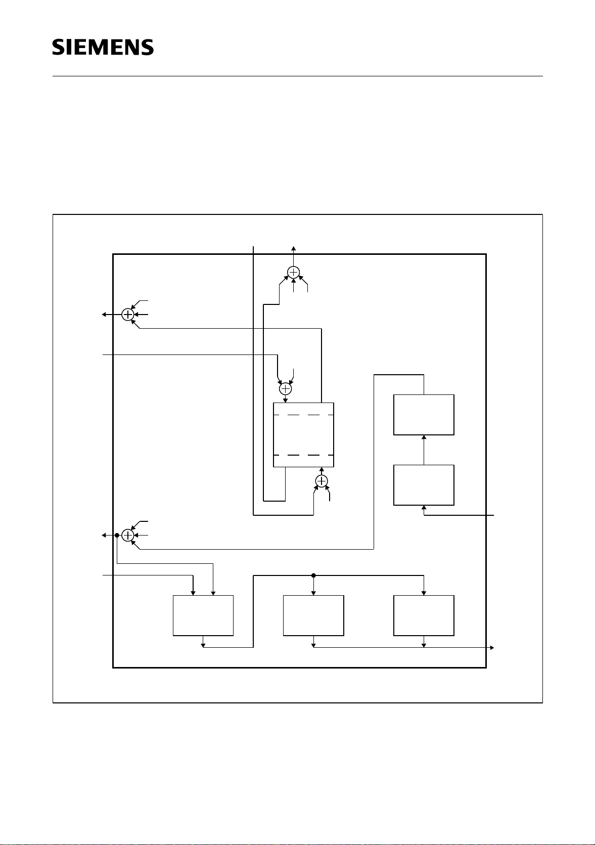
The following figures show the connections for two typical states during operation. Units
that are not needed are not shown. Inputs that are not needed are connected to S
provides silence (denoted by 0). In figure 8 a hands-free phone conversation is currently
in progress. The speech coder is used to record the signals of both parties. The alert tone
detector is used to detect an alerting tone o f an of f-hoo k c all er id request while the CID
decoder decodes the actual data transmitted in this case.
which
0
loud-
speaker
microphone
line
out
line
in
0
0
0
Speech
coder
acoustic side
Speaker-
phone
line side
AGC
0
0
0
Memory
Line Echo
Canceller
CID
decoder
Alert Tone
Detector
SCI
Figure 8 Functional Units - Recording a Phone Conversation
Semiconductor Group 25 10.97
PSB 4860
Functional Description
In figure 9 a phone conv ersation using the speakerpho ne is in progress. One party is
using the base station of a DECT system while the other party is using a mobile handset.
At the same time an external call is serviced by the answering machine. In the current
state a message (recorded or out going) is being played back. In this case the DTMF
detector is used t o detect sign als for remote a ccess while th e CPT detector is u sed to
determine the end of the external call.
®
SSDI/IOM
Channel 1
-2
loud-
speaker
microphone
line
out
line
in
0
0
0
0
00
0
acoustic side
Speaker-
phone
line side
Equalizer
Speech
decoder
0
Memory
Line Echo
Canceller
CPT
decoder
DTMF
Detector
SCI
Figure 9 Functional Units - Simultaneous Internal and External Call
Semiconductor Group 26 10.97
PSB 4860
Functional Description
2.1 Functional Units
In this section the functional units of the PSB 4860 are described in detail. The functional
units can be individually enabled or disabled.
2.1.1 Full Duplex Speakerphone
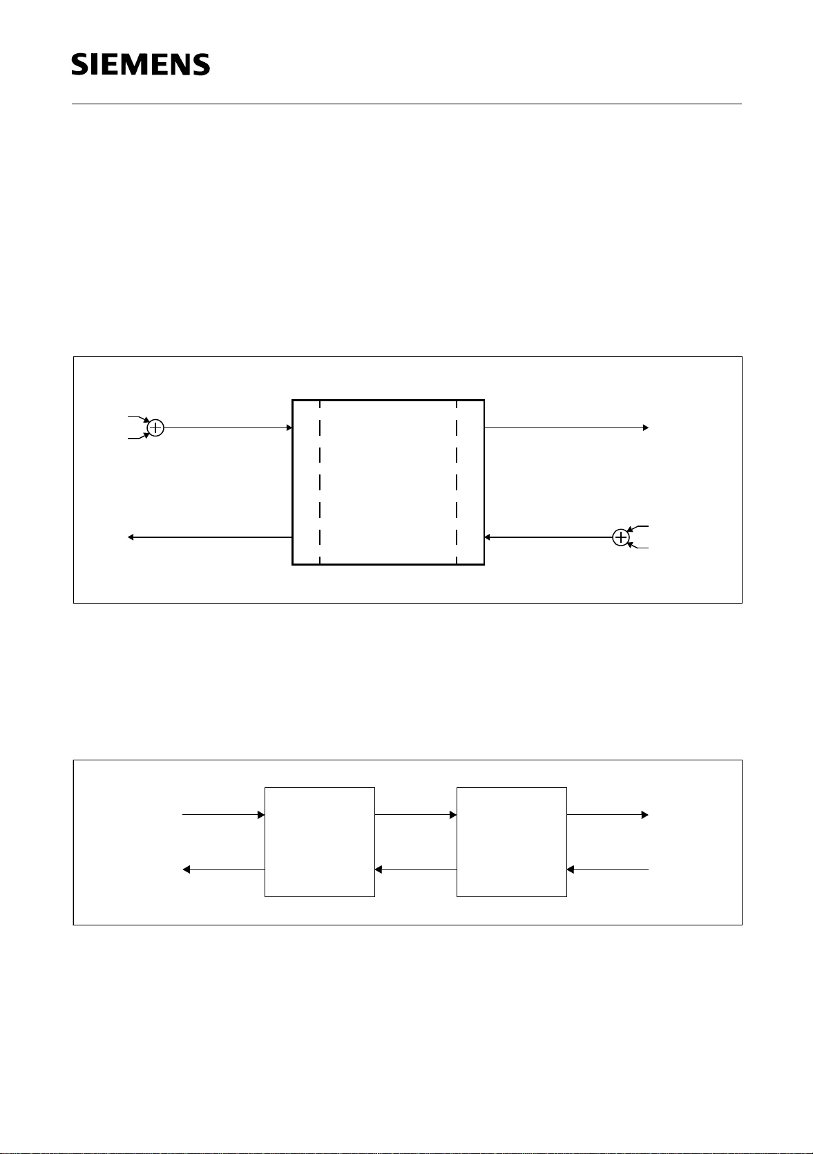
The speakerphone unit (figure 10) is attached to four signals (microphone, loudspeaker,
line out and line in). The two input signals (microphone, line in) are preceded by a signal
summation point.
I
1
I
2
S
11
microphone
loudspeaker
a
c
o
u
s
t
Speakerphone
i
c
s
i
d
e
line out
l
i
n
e
s
i
d
e
line in
S
12
I
3
I
4
Figure 10 Speakerphone - Signal Connections
Internally, this unit can be divided into an echo cancellation unit and an echo suppression
unit (figure 11). The echo cancell ation unit provides the attenuation G
suppression unit provides the attenuation G
speakerphone is therefore ATT=G
C+Gs
.
. The total attenuation ATT of the
s
while the echo
c
Echo
Cancellation
G
loudspeaker line in
c
Echo
Suppression
G
S
line outmicrophone
Figure 11 Speakerphone - Block Diagram
The echo suppression unit can be enabled without the echo cancellation unit. If the echo
cancellation unit is disabled, the echo suppression unit still provides speakerphone
functionality, albeit onl y half duplex. As the echo cancellation must be dis abled during
recording or playback of speech data, this option allows for speakerphone operation
Semiconductor Group 27 10.97
PSB 4860
Functional Description
even if recording or playback is going on. The echo sup pression unit is also used to
provide additional attenuation if the echo cancellation unit cannot provide all of the
required attenuation itself.
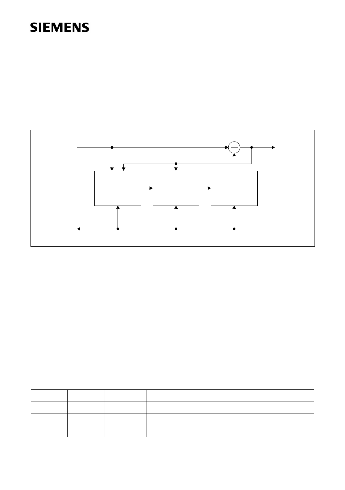
2.1.2 Echo Cancellation A simplified block diagram of the echo cancellation unit is shown in figure 12.
microphone
line out
-
FIR
NLMSControl
loudspeaker
Filter
line in
Figure 12 Echo Cancellation Unit - Block Diagram
The echo cancellation unit consists of an finite impulse response filter (FIR) that models
the expected acoustic echo, an NLMS based adaption unit and a control unit. The
expected echo is subtracted from the actual input signal from the microphone. If the
model is exact and the echo does n ot excee d the len gth of th e filter t hen the e cho can
be completely cancelled. However, even if this ideal state can be achieved for one given
moment the acoustic echo usually changes over time. Therefore the NLMS unit
continuously adapts the coefficients of the FIR filter. This adaption process is steered by
the control unit. As an example, the adaption is inhibited as long as double talk is
detected by the control un it. Fu rthermore t he con trol unit informs the ech o supp ress ion
unit about the achieved echo return loss.
Table 3 shows the registers associated with the echo cancellation unit.
Table 3 Echo Cancellation Unit Registers
Register # of Bits Name Comment
SAELEN 9 LEN Length of FIR filter
SAEATT 15 ATT Attenuation reduction during double-talk
SAEGS 3 GS Global scale (all blocks)
Semiconductor Group 28 10.97
PSB 4860
Functional Description
Table 3 Echo Cancellation Unit Registers
SAEPS1 3 AS Partial scale (for blocks >= SAEPS2:FB)
SAEPS2 3 FB First block affected by partial scale
The length of the FIR filter can be varied from 127 to 511 taps (15.875ms to 63.875ms).
The taps are grouped into blocks. Each block contains 64 taps.
The performance of the FIR filter can be enhanced by p rescaling some or call of the
coefficients of the FIR filter. A coefficient is prescaled by multiplying it by a constant. The
advantage of prescaling is an enhanced precision and consequently an enhanced echo
cancellation. The disadvantage is a reduced echo cancellation performance if the signal
exceeds the maximal coefficient value. More precisely, if a coefficient at tap T
by a factor C
C
(Max: Maximum PCM value). As an example figure shows a typical room impulse
i
then the level of the echo (room impulse response) must not exceed Max/
i
response.
is scaled
i
A
0.5
0.25
t
0.25
t
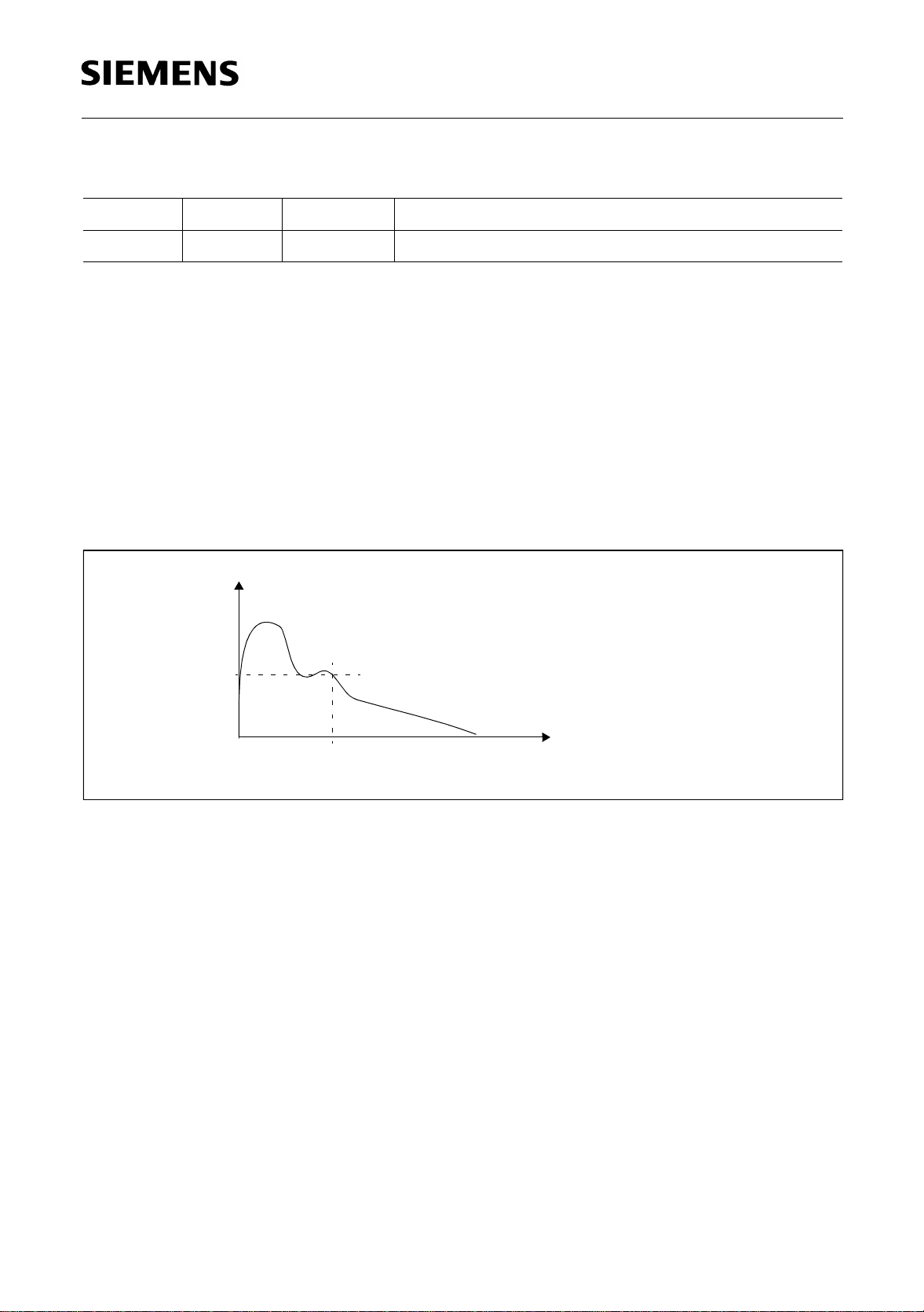
Figure 13 Echo Cancellation Unit - Typical Room Impulse Response
First of all, the echo never exceeds 0.5 of the maximum value. Furthermore the echo
never exceeds 0.25 of the maximum value after time t
be scaled by a factor of 2 and all co efficients fo r taps correspon ding to times af ter t
. Therefore all coefficients can
0.25
0.25
can be scaled a factor of 4.
The echo cancellati on unit provides thre e parameters for scali ng coefficients. Th e first
parameter (GS) determines a scale for all coefficients. The second parameter (FB)
determines the first block for which an additional scale (PS) takes effect.
This feature can be used for different default settings like large or small rooms.
Semiconductor Group 29 10.97
PSB 4860
Functional Description
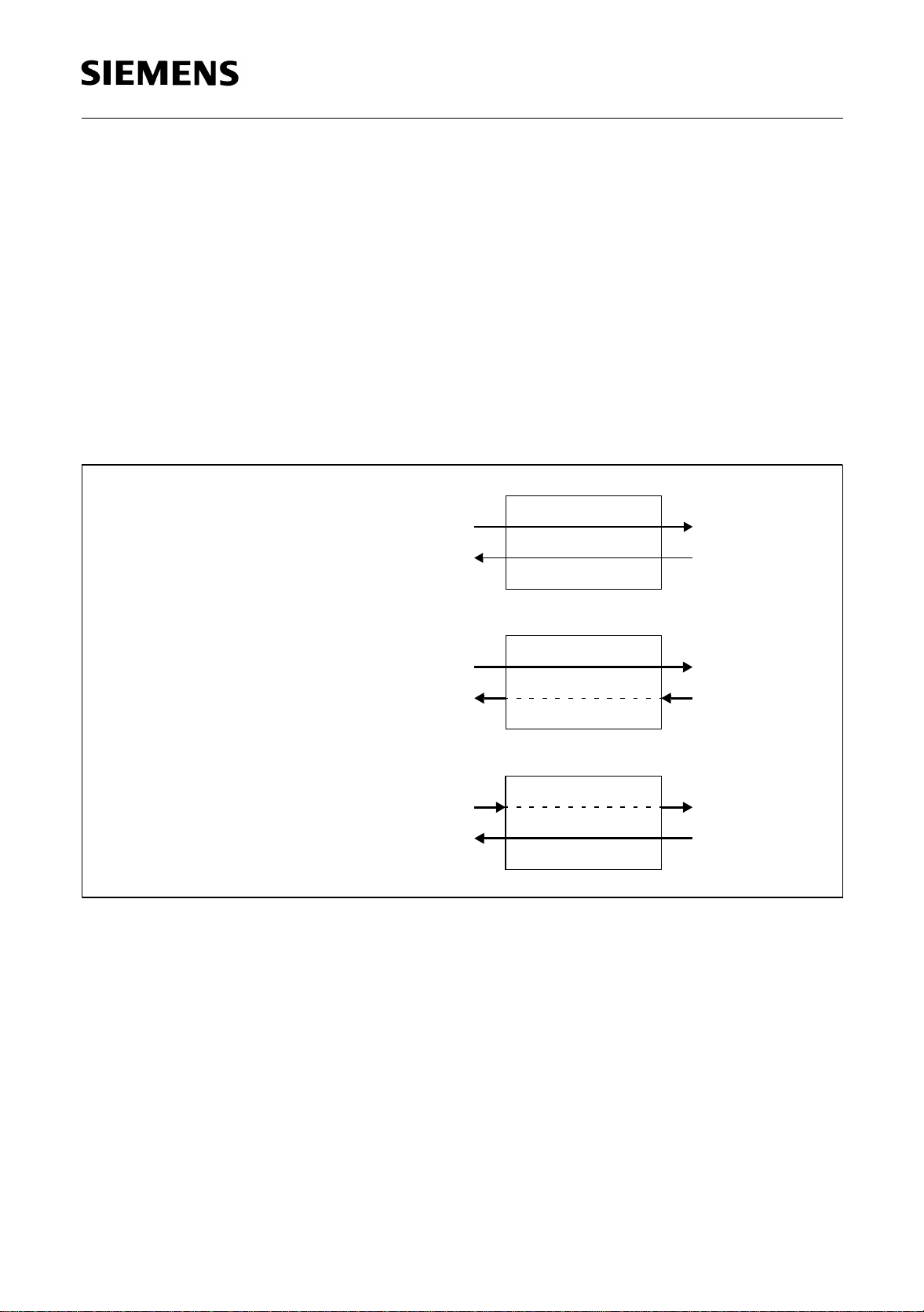
2.1.3 Echo Suppression
The echo suppression unit can be in one of three states:
• transmit state
• receive state
• idle state
In transmit state the microphone signal drives the line output while the line input is
attenuated. In receive state the loudspeaker signa l is driven by the line inp ut while the
microphone signal is attenuated. In idle st ate both signal paths are a ctive with evenly
distributed attenuation.
idle state
microphone
loudspeaker
microphone
transmit state
loudspeaker
microphone
receive stat e
loudspeaker
Figure 14 Echo Suppression Unit - States of Operation
line out
line in
line out
line in
line out
line in
Semiconductor Group 30 10.97

PSB 4860
Functional Description
Figure15 shows the signal flow graph of the echo suppression unit in more detail.
LGAX
SDR
line outmicrophone
SCLSSCAS
AGCR
loudspeaker
AGCX
SDX
Attenuation
LGAR line in
GHX
Control
GHR
Figure 15 Echo Suppression Unit - Signal Flow Graph
State switching is controlled by the speech comparators (SCAS, SCLS) and the speech
detectors (SDX, SDR). The amplifiers (AGCX, AGCR, LGAX, LGAR) are used to
achieve proper signal levels for each state. All blocks are programmable. Thus the
telephone set can be optimized and adjusted to the particular geometrical and acoustical
environment. The following sections discuss each block of the echo suppression unit in
detail.
Semiconductor Group 31 10.97

PSB 4860
Functional Description
2.1.3.1 Speech Detector
For each signal source a speech detector (SDX, SDR) is available. The speech
detectors are identical but ca n be programm ed indiv idually . Figure 16 shows th e sig nal
flow graph of a speech detector.
OFF
-
LIM LP1 PD
LP1
LIM
Signal Preprocessing
PDS
PDN
LP2
LP2S
LP2N
LP2L
Background Noise Monitor
Figure 16 Speech Detector - Signal Flow Graph
The first three units (LIM, LP1, PD) are used for preprocessing the signal while the actual
speech detection is performed by the background noise monitor.
Background Noise Monitor
The tasks of the noise monitor are to differentiate voice signals from background noise,
even if it exceeds the voice level, and to recognize voice signals without any delay.
Therefore the Background Noise Monitor consists of the Low-Pass Filter 2 (LP2) and the
offset in two separate branches. Basically it works on the burst-characteristic of the
speech: voice signals consist of short peaks with high power (bursts). In contrast,
background noise can be regarded approximately stationary from its average power.
Low-Pass Filter 2 provides different time constants for noise (non-detected speech) and
speech. It determines the average of the no ise reference level. In case of bac kground
noise the level at the output of LP2 is approximately the level of the input. As in the other
branch an additional offset OFF is added to the signal, the comparator signals noise. At
speech bursts the digital signals arriving at the comparator via the offset branch change
faster than those via the LP2-branch. If the difference exceeds the offset OFF, the
Semiconductor Group 32 10.97

PSB 4860
Functional Description
comparator signals speec h. Therefore the output of the backgrou nd noise monitor is a
digital signal indicating speech (1) or noise (0).
A small fade constant (LP2N) enables fast settling of LP2 to the average noise level after
the end of speec h re cog niti on. H oweve r, a to o s mall time constant for LP2N can c aus e
rapid charging to such a high level that after recognizing speech the danger of an
unwanted switchin g back to noise exists. It is recommended t o choose a large rising
constant (LP2S) so that spee ch itself charges the LP2 very sl owly. Generally, it is not
recommended to choos e an infini te LP2S because t hen appro aching the noi se level i s
disabled. Duri ng co nti nuou s speech or tones the LP2 will be charge d until the limitation
LP2L is reached. Then the value of LP2 is frozen until a break discharges the LP2. This
limitation permits transmission of continuous tones and “music on hold”.
The offset stage represents the estimated difference between the speech signal and
averaged noise.
Signal Preprocessing
As described in the preceding chapter, the background noise monitor is able to
discriminate betw een spee ch and noise. In very short spee ch p aus es e.g . between two
words, however, it changes immediately to non-speech, which is equal to noise.
Therefore a peak detection is required in front of the Noise Monitor.
The main task of the Peak Detector (PD) is to bridge the very short speech pauses during
a monolog so that this time constant has to be long. Furthermore, the speech bursts are
stored so that a sure speech detection is guaranteed. But if no speech is recognized the
noise low-pass LP 2 must be charged faster to the av erage noise lev el. In additi on, the
noise edges are to be smoothed. The refore two time constants are necessary. As the
peak detector is ve ry sensitive to spikes, the low-pass LP1 filters the inco ming signal
containing noise in a way that main spikes are eliminated. Due to the programmable time
constant it is possible to refuse high-energy sibilants and noise edges.
To compress the speech signals in their amplitudes and to ease the detection of speech,
the signals have t o be compand ed logarithmi cally. Hereby, the spee ch detector s hould
not be influenced by the s ystem noise w hich is always present but shoul d discriminate
between speech and background noise. The limitation of the logarithmic amplifier can be
programmed via the parameter LIM. LIM is related to the maximum PCM level. A signal
exceeding the limitation de fined by LIM is getting amplified logarithmic ally, while very
smooth system noi se bel ow is ne glecte d. It sh oul d be th e leve l o f the m ini mum sy stem
noise which is always existing; in the transmit path the noise generated by the telephone
circuitry itself and in receive direction the level of the first bit which is stable without any
speech signal at the receive path. Table 6 shows the parame ters for the s peech detect or.
Semiconductor Group 33 10.97

PSB 4860
Functional Description
Table 4 Speech Detector Parameters
Parameter # of bytes Range Comment
LIM 1 0 to 95 dB Limitation of log. amplifier
OFF 1 0 to 95 dB Level offset up to detected noise
PDS 1 1 to 2000 ms Peak decrement PD1 (speech)
PDN 1 1 to 2000 ms Peak decrement PD1 (noise)
LP1 1 1 to 2000 ms Time constant LP1
LP2S 1 2 to 250 s Time constant LP2 (speech)
LP2N 1 1 to 2000 ms Time constant LP2 (noise)
LP2L 1 0 to 95 dB Maximum value of LP2
The input signal of the speech detector can be connected to either the input signal of the
echo suppression unit (as shown for SDX) or the output of the associated AGC (as
shown for SDR).
Semiconductor Group 34 10.97

PSB 4860
Functional Description
2.1.3.2 Speech Comparators (SC)
The echo suppression un it has tw o ide ntic al s pee ch comp arato rs (SCAS, SCLS). Eac h
comparator can be programmed individually to accommodate the different system
characteristics of the acoust ic interface and the line interfa ce. As SCAS and SCLS are
identical, the following description holds for both SCAS and SCLS.
The SC has two input signals SX and SR, which map to microphone/loudsp eaker for
SCAS and line in/line out for SCLS.
In principle, the SC works according to the following equation:
if SX > SR + V then switch state
Therefore, SCAS controls the switching to transmit state and SCLS controls the
switching to receive state. Switching is done only if SX exceeds SR by at least the
expected acoustic lev el enhancement V which is divid ed into two parts: G and GD. A
block diagram of the SC is shown in figure 17.
SX
SR
Log. Amp.
Log. Amp. Base Gain Gain Reserve Peak Decrement
G
GDS
GDN
Peak Decrement
PDS
PDN
PDS
PDN
Figure 17 Speech Comparator - Block Diagram
At both inputs, logarithmic amplifiers compress the signal range. Hence after the
required signal processing for con trolling the acoustic echo, pure logarithmic levels on
both paths are compared.
The main task of the comparator is to control the echo. The internal coupling due to the
direct sound and mechanical resonances are covered by G. The external coupling,
mainly caused by the acoustic feedback, is controlled by GD/PD.
Semiconductor Group 35 10.97

PSB 4860
Functional Description
The base gain (G) correspo nds to th e terminal couplin gs of the complete telephone: G
is the measured or calculated level enhancement between both receive and transmit
inputs of the SC.
To control the acoustic feedback two parameters are necessary: GD represents the
actual reserve on the measured G. Together with the Peak Decrement (PD) it simulates
the echo behavior at the acoustic s ide: After speech has ended there is a short time
during which hard couplings through the mechanics and resonances and the direct echo
are present. Till the end of that time (∆
to G to prevent clipping caused by these internal couplings. Then, only the acoustic
feedback is present. This coup ling, however, is reduced by air atte nuation. For this in
general the longer the dela y, the smaller the echo being valid. This echo behavior is
featured by the decrement PD.
t) the level enhancement V must be at least equal
dB
GD*
PD*
GD
G
RX-Speech
PD
G
RX-noise
∆t
Figure 18 Speech Comparator - Interdependence of Parameters
t
According to figure 18 , a compromis e between the re serve GD and th e decrement PD
has to be made: a smaller reserve (GD) above the level enhancement G requires a
longer time to decrease (PD). It is easy to overshout the other side but the
intercommunication is harder because after the end of the speech, the level of the
estimated echo has to be exceeded. In contrary, with a higher reserve (GD*) it is harder
to overshout continuous speech or tones, but it enables a faster intercommunication
because of a stronger decrement (PD*).
Semiconductor Group 36 10.97

PSB 4860
Functional Description
Two pairs of coefficients, GDS/PDS when speech is detected, and GDN/PDN in case of
noise, offer a different echo handling for speech and non-speech.
With speech, even if very strong resonances are present, the performance will not be
worsened by the high GDS needed. Only when speech is detected, a high reserve
prevents clipping. A time period ET [ms] after speech end, the parameters of the
comparator are switched to the “noise” values. If both sets of the parameters are equal,
ET has no function.
Table 5 Speech Comparator Parameters
Parameter # of bytes Range Comment
G 1 – 48 to + 48 dB Base Gain
GDS 1 0 to 48 dB Gain Reserve (Speech)
PDS 1 0.025 to 6 dB/ms Peak Decrement (Speech)
GDN 1 0 to 48 dB Gain Reserve (Noise)
PDN 1 0.025 to 6 dB/ms Peak Decrement (Noise)
ET 1 0 to 992 ms Time to Switch from speech to noise
parameters
2.1.3.3 Attenuation Control
The attenuation control unit controls the attenuation stages GHX and GHR and performs
state switching. The programmable attenuation ATT is completely switched to GHX
(GHR) in receive state (transmit state). In idle state bot h GHX and GHR attenuate by
ATT/2.
In addition, a ttenuation is also influ enced by the auto matic ga in control stage s (AGCX,
AGCR).
State switching depends on the signals of one speech comparator and the
corresponding speec h detector. While each state is as sociated with the programmed
attenuation, the time is takes to reach th e steady-state atte nuation after a state switch
can be programmed (T
SW).
If the current state is either transmit or receive and n o speech on e ither side has been
detected for time T
then idle state is entered. To smoothen the transition, the
W
attenuation is incremented (decremented) by DS until the evenly di stribution ATT/2 for
both GHX and GHR is reached.
Table 6 shows the paramete rs for the attenua tion unit. Note that T
the current attenuation by the formula .
Semiconductor Group 37 10.97
T
sw
SW ATT×=
is dependent on
SW

Table 6 Attenuation Control Unit Parameters
Parameter # of bytes Range Comment
PSB 4860
Functional Description
TW 1 16 ms to 4 s T
to return to idle state
W
ATT 1 0 to 95 dB Attenuation for GHX and GHR
DS 1 0.6 to 680 ms/dB Decay Speed (to idle state)
SW 1 0.0052 to 10 ms/dB Decay Rate (used for T
SW
)
Note: In addition, attenua tion is also influenced by the Automa tic Gain Control stages
(AGCX, AGCR) in order to keep the total loop attenuation constant.
2.1.3.4 Echo Suppression Status Output
The PSB 4860 can report the current state of the echo suppression unit to ease
optimization of the parameter set of the echo suppression unit. In this case the SPS
SPS
pins are set according to table 7.
1
and
0
Table 7 SPS Output Encoding
SPS
0
SPS
Echo Suppression Unit State
1
0 0 no echo suppression operation
0 1 receive
10transmit
1 1 idle
Furthermore the controller can read the current value of the SPS pins by reading register
SPSCTL.
2.1.3.5 Loudhearing
The speakerphone unit can also be used for controlled loudhearing. If enabled in
loudhearing mode, the loudspeaker amplif ier of the PSB 4851 (ALS) is used instead of
GHR (figure 15) when appropriate to avoid oscillation. In order to enable this feature, the
PSB 4851 must be programmed to a llow ALS override. The ALS field within the AFE
control register AFECTL defines the value sent to the PSB 4851 if attenuation is
necessary (see specification of the PSB 4851).
2.1.3.6 Automatic Gain Control
The echo suppression unit has two identical automatic gain control units (AGCX,
AGCR).
Semiconductor Group 38 10.97

PSB 4860
Functional Description
Operation of the AGC depends on a threshold level defined by the parameter COM
(value relative to the maximum PCM-value). The regulation speed is controlled by
SPEEDH for signal amplitudes above the threshold and SPEEDL for amplitudes below.
Usually SPEEDH will be chosen to be at least 10 times faster than SPEEDL. The bold
line in Figure 19 depicts th e steady-state output level of the AGC as a function of the
input level.
-10 dB-20 dB
AG_ATT
Example:
COM
AG_GAIN
AG_ATT
=
=
=
AGC input level
-30 dB
15 dB
20 dB
AG_GAIN
Figure 19 Echo Suppression Unit - Automatic Gain Control
max. PCM
-10 dB
-20 dB
COM
AGC
output
level
For reasons of physiological acceptance the AGC gain is automatically reduced in case
of continuous backg round noi se (e.g. by ventil ators). The reduc tion is programme d via
the NOlS parameter. When the noise level exceeds the threshold determined by NOIS,
the amplification will be reduced by the same amount the noise level is above the
threshold. The current gain/attenuation of the AGC can be read at any time (AG_CUR).
An additional low pass with time constant LP is provided to avoid an immediate response
of the AGC to very short signal bursts.
If SDX detects noise , AGCX is not working. In this case the last gain setting is used.
Regulation starts with this value as soon as SDX detects speech.
Likewise, if SDR detects noise, AGCR is not working. In this case the last gain setting is
used. Regulation starts with this value as soon as SDR detects speech. When the AGC
has been disabled the initial gain used immediately after enabling the AGC can be
programmed. Table 8 shows the parameters of the AGC.
Semiconductor Group 39 10.97

PSB 4860
Functional Description
Table 8 Automatic Gain Control Parameters
Parameter # of Bytes Range Comment
AG_INIT 1 -95 dB to 95dB Initial AGC gain/attenuation
COM 1 0 to – 95 dB Compare level rel. to max. PCM-value
AG_ATT 1 0 to -95 dB Attenuation range
AG_GAIN 1 0 to 95 dB Gain range
AG_CUR 1 -95 dB to 95 dB Current gain/attenuation
SPEEDL 1 0.25 to 62.5 dB/s Change rate for lower levels
SPEEDH 1 0.25 to 62.5 dB/s Change rate for higher levels
NOIS 1 0 to – 95 dB Threshold for AGC-reduction
by background noise
LP 1 0.025 to 16 ms AGC low pass time constant
Note: There are two sets of parameters, one for AGCX and one for AGCR.
Note: By setting AG_GAIN to 0 dB a limitation function can be realized with the AGC.
2.1.3.7 Fixed Gain
Each signal path features an additional amplifier (LGAX, LGAR) that can be set to a fixed
gain. These amplifiers should be used for the basic amplification in order to avoid
saturation in the preceding stages. Table 9 shows the only parameter of this stage.
Table 9 Fixed Gain Parameters
Parameter # of Bytes Range Comment
LGA 1 -12 dB to 12 dB always active
2.1.3.8 Mode Control Table 10 shows the registers used to determine the signal sources and the mode.
Table 10 Speakerphone Control Registers
Register # of Bits Name Comment
SCTL 1 ENS Echo suppression unit enable
SCTL 1 ENC Echo cancellation unit enable
SCTL 1 MD Speakerphone or loudhearing mode
SCTL 1 AGX AGCX enable
Semiconductor Group 40 10.97

Table 10 Speakerphone Control Registers
SCTL 1 AGR AGCR enable
SCTL 1 SDX SDX input tap
SCTL 1 SDR SDR input tap
AFECTL 4 ALS ALS value for loudhearing
SSRC1 5 I1 Input signal 1 (microphone)
SSRC1 5 I2 Input signal 2 (microphone)
SSRC2 5 I3 Input signal 3 (line in)
SSRC2 5 I4 Input signal 4 (line in)
PSB 4860
Functional Description
Semiconductor Group 41 10.97

PSB 4860
Functional Description
2.1.4 Line Echo Canceller
The PSB 4860 contains an adaptive line echo cancella tion unit for the cancellation of
near end echoes. The unit h as two modes: normal an d extended. In normal mod e, the
maximum echo length is 4 ms. This mode is alw ays available. In extended mode , the
maximum echo length is 24 ms. Extended mode cannot be used while the speech
encoder, the echo cancellation unit or slow playback is active.
The line echo cancellation unit is especially useful in front of the various detectors
(DTMF, CPT, etc.). A block diagram is shown in figure 20.
I
2
+
Σ
S
15
-
Adaptive
Filter
I
1
Figure 20 Line Echo Cancellation Unit - Block Diagram
The line echo cancelle r provides only one ou tgoing signal (S
signal would be identical with the input signal I
Input I
is usually connected to the l ine inpu t w hile inp ut I1 is connected to the outgoing
2
.
1
) as the other outgoing
15
signal.
In normal mode the adaption process can be controlled by three parameters: MIN, ATT
and MGN. Adaption takes only place if both of the following conditions hold:
I1 MIN>
1.
I1 I2–ATTMGN+–0>
2.
With the first con diti on ada ption to sma ll signal s can be avoid ed. The s econd condit ion
avoids adaption during double talk. The parameter ATT represents the echo loss
provided by external circuitry. The adaption stops if the power of the received signal (I2)
exceeds the power of the expected signal (I1-ATT) by more than the margin MGN.
Semiconductor Group 42 10.97

PSB 4860
Functional Description
Table 11 shows the registers associated with the line echo canceller.
Table 11 Line Echo Cancellation Unit Registers
Register # of Bits Name Comment Relevant
Mode
LECCTL 1 EN Line echo canceller enable both
LECCTL 1 MD Line echo canceller mode
LECCTL 5 I2 Input signal selection for I
LECCTL 5 I1 Input signal selection for I
LECLEV 15 MIN Minimal power for signal I
2
1
1
LECATT 15 ATT Externally provided attenuation (I
to I2) normal
1
both
both
normal
LECMGN 15 MGN Margin for double talk detection normal
Semiconductor Group 43 10.97

PSB 4860
Functional Description
2.1.5 DTMF Detector
Figure 21 shows a block dia gram of the D TMF det ector. The results of the detector are
available in the status register and a dedicated resul t register that can be re ad via the
serial control interface (SCI) by the external controller. All sixteen standard DTMF tones
are recognized.
I
1
DTMF
Recognition
SCI
Figure 21 DTMF Detector - Block Diagram
Table 12 to 14 show the associated registers.
Table 12 DTMF Detector Control Register
Register # of Bits Name Comment
DDCTL 1 EN DTMF detector enable
DDCTL 5 I1 Input signal selection
As soon as a v ali d DTMF tone is reco gni zed, the status w ord a nd the DTMF tone c ode
are updated (table 13).
Table 13 DTMF Detector Results
Register # of Bits Name Comment
STATUS 1 DTV DTMF code valid
DDCTL 5 DTC DTMF tone code
DTV is set when a DTMF tone is recognized and reset when no DTMF tone is recognized
or the detector is disabled. The code for the DTMF tone is placed into the register
DDCTL. The registers DDTW and DDLEV hold parameters for detection (table 14).
Table 14 DTMF Detector Parameters
Register # of Bits Name Comment
DDTW 15 TWIST Twist for DTMF recognition
DDLEV 6 MIN Minimum signal level to detect DTMF tones
Semiconductor Group 44 10.97

PSB 4860
Functional Description
2.1.6 CNG Detector
The calling tone (C NG) detector c an detect the standard calling tone s of fax m achines
or modems. This helps to distinguish voice messages from data transfers. The result of
the detector is available in the status register that can be read via the serial control
interface (SCI) by the exte rnal con troller. The CNG d etector cons ists of tw o band-pas s
filters with fixed center frequency of 1100 Hz and 1300 Hz.
CNG Detector
I
1
1100 Hz 1300 Hz
SCI
Figure 22 CNG Detector - Block Diagram
Table 15 shows the available parameters.
Table 15 CNG Detector Registers
Register # of Bits Name Comment
CNGCTL 1 EN CNG detector enable
CNGCTL 5 I1 Input signal selection
CNGLEV 16 MIN Minimum signal level
CNGBT 16 TIME Minimum time of signal burst
CNGRES 16 RES Input signal resolution
Both the programmed mini mum time and the mi nimum signal level m ust be exceeded
for a valid CNG tone. Furthermore the input signal resolution can be reduced by the RES
parameter. This can be useful in a noisy env ironment at low signal levels although the
accuracy of the detect ion decreases. As soo n as a valid tone is recognized, t he status
word of the PSB 4860 is updated. The status bits are defined as follows:
Table 16 CNG Detector Result
Register # of Bits Name Comment
STATUS 1 CNG Fax/Modem calling tone detected
Semiconductor Group 45 10.97

PSB 4860
Functional Description
2.1.7 Alert Tone Detector
The alert tone detector can detect the st andard alert tones (2130 Hz and 2750 Hz) for
caller id protocols. The results of the detector are available in the status register and the
dedicated regist er ATDCTL 0 that c an be re ad via the ser ial cont rol int erface (SCI) by the
external controller.
I
1
Detector
SCI
Figure 23 Alert Tone Detector - Block Diagram
Table 17 Alert Tone Detector Registers
Register # of Bits Name Comment
ATDCTL0 1 EN Alert Tone Detector Enable
ATDCTL0 5 I1 Input signal selection
ATDCTL1 1 MD Detection of dual tones or single tones
ATDCTL1 1 DEV Maximum deviation (0.5% or 1.1%)
ATDCTL1 8 MIN Minimum signal level to detect alert tones
Alert Tone
As soon as a valid alert tone is recognized, the status word of the PSB 4860 and the code
for the detected combination of alert tones are updated (table 18).
Table 18 Alert Tone Detector Results
Register # of Bits Name Comment
STATUS 1 ATV Alert tone detected
ATDCTL0 2 ATC Alert tone code
Semiconductor Group 46 10.97

PSB 4860
Functional Description
2.1.8 CPT Detector
The selected signal is monitored continuously for a call progress tone. The CPT detector
consists of a band-pass and an optional timing checker (figure 24).
Band-pass
1
300-640 Hz
SCI (Status)I
Timing
Checker
Figure 24 CPT Detector - Block Diagram
The CPT detector can be used in two modes: raw and cooked. In raw mode, the
occurrence of a signal within the frequency range, time and energy limits is directly
reported. The timing checker is bypassed and therefore the PSB 4860 does not interpret
the length or interval of the signal.
In cooked mode, the number and duration of sig nal bursts are interpreted by th e t imin g
checker. A signal burst f ollowed by a gap is called a cycle. Cooked mode req uires a
minimum of two cycles. The CPT flag is set with the first burst after the programmed
number of cycles has been detected. The CPT flag remains set until the unit is disabled,
even if the conditions are not met anymore. In this mode the CPT is modelled as a
sequence of identical bursts separated by gaps with identical length. The PSB 4860 can
be programmed to accept a range for bo th the burst and the gap. It is also poss ible to
specify a maximum aberration of two consecutive bursts and gaps. Figure 25 shows the
parameters for a single cycle (burst and gap).
t
Bmin
Bmax
t
Gmin
t
Gmax
t
Figure 25 CPT Detector - Cooked Mode
The status bit is defined as follows:
Semiconductor Group 47 10.97

PSB 4860
Functional Description
Table 19 CPT Detector Result
Register # of Bits Name Comment
STATUS 1 CPT CP tone currently detected [340 Hz; 640 Hz]
CPT is not affected by reading the status word. It is automatically reset when the unit is
disabled. Table 20 shows the control register for the CPT detector.
Table 20 CPT Detector Registers
Register # of Bits Name Comment
CPTCTL 1 EN Unit enable
CPTCTL 1 MD Mode (cooked, raw)
CPTCTL 5 I1 Input signal selection
CPTMN 8 MINB Minimum time of a signal burst (t
CPTMN 8 MING Minimum time of a signal gap (t
Gmin
CPTMX 8 MAXB Maximum time of a signal burst (t
CPTMX 8 MAXG Maximum time of a signal gap (t
Bmin
Bmax
Gmax
)
)
)
)
CPTDT 8 DIFB Ma xim um diffe renc e betw een con sec uti ve burst s
CPTDT 8 DIFG Maxim um diffe renc e between consecutive gaps
CPTTR 3 NUM Number of cycles (cooked mode), 0 (raw mode)
CPTTR 8 MIN Minimum signal level to detect tones
CPTTR 4 SN Minimal signal-to-noise ratio
If any condition is violated during a sequen ce of c ycles t he timing checke r is reset and
restarts with the next valid burst.
Note: In cooked mode CPT is se t with the first burst after the pro grammed number of
cycles has been detected.
Note: The number of cycles must be set to zero in raw mode.
Semiconductor Group 48 10.97

PSB 4860
Functional Description
2.1.9 Caller ID Decoder
The caller ID decoder i s basically a 1200 baud modem (FSK, demodu lation only). Th e
bit stream is formatted by a subsequent UART and the data is available in a data register
along with status information (figure 26).
I
1
FSK demod.
(Bellcore, V.23)
UART
SCI (Status, Data)
Figure 26 Caller ID Decoder - Block Diagram
The FSK demodulator supports two modes according to table 21. The appropriate mode
is detected automatically.
Table 21 Caller ID Decoder Modes
Mode Mark
(Hz)
Space
(Hz)
Comment
1 1200 2200 Bellcore
2 1300 2100 V.23
The CID decoder does not interpret the data received. Each byte received is placed into
the CIDCTL register (table 23). The status byte of the PSB 4860 is updated (table 22).
Table 22 Caller ID Decoder Status
Register # of Bits Name Comment
STATUS 1 CIA CID byte received
STATUS 1 CD Carrier Detected
CIA and CD are cleared when the unit is disabled. In addition, CIA is cleared when
CIDCTL0 is read.
Table 23 Caller ID Decoder Registers
Register # of Bits Name Comment
CIDCTL0 1 EN Unit enable
CIDCTL0 5 I1 Input signal selection
CIDCTL0 8 DATA Last CID data byte received
Semiconductor Group 49 10.97

PSB 4860
Functional Description
Table 23 Caller ID Decoder Registers
Register # of Bits Name Comment
CIDCTL1 5 NMSS Number of mark/space sequences necessary for
successful detection of carrier detect
CIDCTL1 6 NMB Number of mark bits necessary before space of first
byte after carrier detect
CIDCTL1 5 MIN Minimum signal level for CID detection
When the CID unit is enabl ed, it first waits for a channel sei zure signal consisti ng of a
series of alternating space and mark signals. The number of spaces and marks that have
to be received without errors before the PSB 4860 reports a carrier det ect by setting
status bit CD can be programmed.
Channel seizure must be followed by at least 16 continuous mark signals. The first space
signal detected is then regarded as the start bit of the first message byte.
The interpretation of the data, including message type, length and checksum is
completely left to the controller. The CID unit should be disabled as soon as the complete
information has been received as it cannot detect the end of the transmission by itself.
Note: Some caller ID mechanis m may require additional external compon ents for DC
decoupling. These tasks must be handled by the controller.
Note: The controller is responsible for selecting and storing parts of the CID as needed.
Semiconductor Group 50 10.97

PSB 4860
Functional Description
2.1.10 DTMF Generator
The DTMF generator can g enerate single or dual to nes with programmable frequency
and gain. This unit is pr imari ly used to gen erate the co mmon D TMF ton es but ca n also
be used for signalling or other user defined tones. A block diagram is shown in figure 27.
f
1
generator
f
2
generator
gain1
gain2
att1
att2
S
9
S
10
Figure 27 DTMF Generator - Block Diagram
Both generators and amplifiers are identical. There are two modes for programming the
generators, cooked mode and raw mode. In cooked mode, the standard DTMF
frequencies are generated by programming a single 4 bit code. In raw mode, the
frequency of each generator/amplifier can be programmed i ndividually by a separate
register. The unit h as two outputs which provide the same signal but with indivi dually
programmable attenuation. Table 24 shows the parameters of this unit.
Table 24 DTMF Generator Registers
Register # of Bits Name Comment
DGCTL 1 EN Enable for generators
DGCTL 1 MD Mode (cooked/raw)
DGCTL 4 DTC DTMF code (cooked mode)
DGF1 15 FRQ1 Frequency of generator 1
DGF2 15 FRQ2 Frequency of generator 2
DGL 7 LEV1 Level of signal for generator 1
DGL 7 LEV2 Level of signal for generator 2
DGATT 8 ATT1 Attenuation of S
DGATT 8 ATT2 Attenuation of S
9
10
Note: DGF1 and DGF2 are undefined when cooked mode is used and must not be
written.
Semiconductor Group 51 10.97

2.1.11 Speech Coder
PSB 4860
Functional Description
The speech coder (figure 28) has two input signals I
and I2. The first signal (I1) is fed to
1
the coder while the second signal (I2 ) is used as a reference signal fo r voice co ntrolled
recording. The si gnal I
can be coded by eith er a High Quality coder or a Long Play
1
coder.
I
1
MIN
I
2
LP
HQ
10300 bit/s
Memory
LP
3300 bit/s
Figure 28 Speech Coder - Block Diagram
In High Quality the ou tput data stream run s at a fixed rate of 1 0300 bit/s and p rovides
excellent speech qual ity. In Long Pla y mode, the ou tput data strea m is further reduc ed
to an average of 3300 bit/s while still maintaining good quality.
Data is written starting at the current file pointer and the file pointer is advanced as
needed. In case of any m emory e rror (e. g. mem ory full ) a fil e erro r is i ndicate d and the
coder is disabled. The controller must subsequently close the file.
The coder can be switched on the fly. However, it may take up to 60 ms until the switch
is executed. The controller must therefore wait for at least this time until issuing another
command that relies on the mode switch. No audio data is lost during switching.
The signal I
is first filtered by a low pass LP1 with programmable time constant and then
2
compared to a reference level MIN. If the filtered signal exceeds MIN, then the status bit
SD (table 25) is set immediately. If the filtered signal has been smaller than MIN for a
programmable time TIME then the status bit SD is reset.
The coder can be enabled in permanent mode or in voice recognition mode. In
permanent mode, the coder starts immediately and compresses all input data
continuously. The current state of the status bit SD does not affect the coder.
In voice recognition mode, the coder is automatically started on the first transition of the
status bit from 0 to 1. Once the coder has started it remains active until disabled.
Table 25 Speech Coder Status
Register # of Bits Name Comment
STATUS 1 SD Speech detected
Semiconductor Group 52 10.97

Functional Description
The operation of the speech coder is defined according to table 26.
Table 26 Speech Coder Registers
Register # of Bits Name Comment
SCCTL 1 EN Enable speech coder
SCCTL 1 HQ High quality mode
SCCTL 1 VC Voice controlled recording
SCCTL 5 I1 Input signal 1 selection
SCCTL 5 I2 Input signal 2 selection
SCCT2 8 MIN Minimal signal level for speech detection
SCCT2 8 TIME Minimum time for reset of SD
SCCT3 8 LP Time constant for low-pass
PSB 4860
Note: The peak data rate in LP mode is 4800 bit/s.
Note: Both HQ and LP mode will not produce identical bit streams after a coding/
decoding cycle.
Semiconductor Group 53 10.97

PSB 4860
Functional Description
2.1.12 Speech Decoder
The speech decoder (figure 29) decompresses the data previously coded by the speech
coder unit and delivers a standard 128 kbit/s data stream.
HQ
10300 bit/s
Memory
LP
3300 bit/s
S
13
Figure 29 Speech Decoder - Block Diagram
The decoder supports fast (1.5 and 2.0 times) and slow (0.5 times) motion independent
of the selected quality. Th e decoder requests input data as n eeded at a variable rate.
Table 27 shows the signal and mode selection for the speech decoder.
Table 27 Speech Decoder Registers
Register # of Bits Name Comment
SDCTL 1 EN Enable speech decoder
SDCTL 2 SPEED Selection of playback speed
Data reading starts at the l ocation of the current file po inter. The file p ointer is upda ted
during speech decoding. If the end of the file is reached, the deco der is automatically
disabled. The PSB 4860 automatically resets SDCTL:EN at this point.
Semiconductor Group 54 10.97

PSB 4860
Functional Description
2.1.13 Analog Front End Interface There are two identical interfaces at the analog side (to PSB 4851) as shown in figure 30.
Channel 2
S
4
IG4
I
1
I
2
I
3
S
3
S
line out
line in IG1
2
Channel 1
IG2
HP IG3 HP
I
1
I
2
I
3
S
1
loudspeaker
microphone
Figure 30 Analog Front End Interface - Block Diagram
For each signal a n ampl ifier is pr ovided for le vel a djustme nt. The in coming signa ls ca n
be passed through an optional high-pass (HP). This high-pas s (f
=20 Hz) is useful for
g
blocking DC offsets and should be enabled by default. Furthermore , up to thre e sig nals
can be mixed in order to generate the outgoing signals (S
). Table 28 shows the
2,S4
associated registers.
Table 28 Analog Front End Interface Registers
Register # of Bits Name Comment
IFG1 16 IG1 Gain for IG1
IFG2 16 IG2 Gain for IG2
IFS1 1 HP High-pass for S
1
IFS1 5 I1 Input signal 1 for IG2
IFS1 5 I2 Input signal 2 for IG2
IFS1 5 I3 Input signal 3 for IG2
IFG3 16 IG3 Gain for IG3
IFG4 16 IG4 Gain for IG4
IFS2 1 HP High-pass for S
3
IFS2 5 I1 Input signal 1 for IG4
IFS2 5 I2 Input signal 2 for IG4
IFS2 5 I3 Input signal 3 for IG4
Semiconductor Group 55 10.97

PSB 4860
Functional Description
2.1.14 Digital Interface
There are two almost ident ical interfaces at the digital side as shown in fi gure 31. The
only difference between these two inte rfaces is that only channel 1 sup ports the SSDI
mode.
Channel 2 (IOM®-2 Interface)Channel 1 (SSDI/IOM®-2 Interface)
I
1
S
6
ATT1
HP
I
2
I
3
S
5
S
8
ATT2
HP
I
1
I
2
I
3
S
7
Figure 31 Digital Interface - Block Diagram
Each outgoing signal c an b e the s um of tw o sign als w ith no a tten uation a nd one sig nal
with programmable attenu ation (ATT). The attenuator can be u sed for artificial echo if
there is none externally provided (e.g. ISDN application). Each input can be passed
through an optional high-pass (HP). The associated registers are shown in table 29.
Table 29 Digital Interface Registers
Register # of Bits Name Comment
IFS3 5 I1 Input signal 1 for S
IFS3 5 I2 Input signal 2 for S
IFS3 5 I3 Input signal 3 for S
IFS3 1 HP High-pass for S
IFS4 5 I1 Input signal 1 for S
IFS4 5 I2 Input signal 2 for S
IFS4 5 I3 Input signal 3 for S
IFS4 1 HP High-pass for S
Semiconductor Group 56 10.97
6
6
6
5
8
8
8
7

PSB 4860
Functional Description
Table 29 Digital Interface Registers
Register # of Bits Name Comment
IFG5 8 ATT1 Attenuation for input signal I3 (Channel 1)
IFG5 8 ATT2 Attenuation for input signal I3 (Channel 2)
Semiconductor Group 57 10.97

PSB 4860
Functional Description
2.1.15 Universal Attenuator
The PSB 4860 contains an universal attenuator that can be connected to any signal (e.g.
for sidetone gain in ISDN applications).
I
1
UA
Figure 32 Universal Attenuator - Block Diagram
Table 30 shows the associated register.
Table 30 Universal Attenuator Registers
Register # of Bits Name Comment
UA 8 ATT Attenuation for UA
UA 5 I1 Input signal for UA
S
14
Semiconductor Group 58 10.97

PSB 4860
Functional Description
2.1.16 Automatic Gain Control Unit
In addition to the universal attenuator with programmable but fixe d gain the PSB 4860
contains an amplifier with auto matic gain control (AGC). The AGC is preceeded by a
signal summation point for two input signals. One of the input signals can be attenuated.
I
1
I
2
ATT
AGC
S
16
S
17
Figure 33 Automatic Gain Control Unit - Block Diagram
Furthermore the signal after the summation point is available. Besides providing a
general signal summation (S
provides the input signal for the speech coder. In this case S
not used) this signal is esp ecially useful if t he AGC unit
16
can be used as a
17
reference signal for voice controlled recording.
The operation of the AGC is similar to AGCX (ACCR) of the speakerphone. The
differences are as follows:
• No NOIS parameter
• Separate enable/disable control
• Slightly different coefficient format
Furthermore the AGC contains a co mparator that starts and stops the gain regulation.
The signal after the summation point (S17) is filtered by a peak detector with time
constant DEC for decay. Then the signal is compared to a programmable limit LIM.
Regulation takes only place when the filtered signal exceeds the limit.
Table 31 shows the associated registers.
Table 31 Automatic Gain Control Registers
Register # of Bits Name Comment
AGCCTL 1 EN Enable
AGCCTL 5 I1 Input signal 1 for AGC
AGCCTL 5 I2 Input signal 2 for AGC
AGCATT 15 ATT Attenuation for I
2
AGC1 8 AG_INIT Initial AGC gain/attenuation
AGC1 8 COM Compare level rel. to max. PCM-value
Semiconductor Group 59 10.97

Functional Description
Table 31 Automatic Gain Control Registers
Register # of Bits Name Comment
AGC2 8 SPEEDL Change rate for lower levels
AGC2 8 SPEEDH Change rate for higher level
AGC3 8 AG_ATT Attenuation range
AGC3 7 AG_GAI N Gain range
AGC4 7 DEC Peak detector time constant
AGC4 8 LIM Comparator minimal signal level
AGC5 7 LP AGC low pass time constant
PSB 4860
Semiconductor Group 60 10.97

PSB 4860
Functional Description
2.1.17 Equalizer
The PSB 4860 also provides an equalizer that can be inserted into any signal path. The
main application for t he e qua liz er is the adaption to the frequenc y c hara cte ri sti cs of the
microphone, transducer or loudspeaker.
The equalizer consists of an IIR filter followed by an FIR filter as shown in figure 34.
-1
I
A1 A2 A9
z
-1
z
D1 D2 D17
-1
z
-1
z
-1
z
IIR
S
18
FIR
C2
-1
z
B2B9
C1
-1
z
-1
z
-1
z
Figure 34 Equalizer - Block Diagram
The coefficients A
C
belong to the FIR filter. Table 32 shows the registers associated with the equalizer.
2
, B2-B9 and C1 belong to the IIR filter, the coefficients D1-D17 and
1-A9
Table 32 Equalizer Registers
Register # of Bits Name Comment
FCFCTL 1 EN Enable
FCFCTL 5 I Input signal for equalizer
FCFCTL 6 ADR Filter coefficient address
FCFCOF 16 Filter coefficient data
Semiconductor Group 61 10.97

PSB 4860
Functional Description
Due to the multitude of coefficie nts the use s an indirec t address ing sche me for reading
or writing an individual coefficient. The ad dress of the coeffic ient is given by ADR and
the actual value is read or written to register FCFCOF.
In order to ease programming the PSB 4860 automatically increments the address ADR
after each access to FCFCOF.
Note: Any access to an out-of-range address automatically resets FCFCTL:ADR.
Semiconductor Group 62 10.97

PSB 4860
Functional Description
2.2 Memory Management
Memory Management
Memory Management - General
This section describes the mem ory management provided by the PSB 4860. As figure
35 shows, three units can access the exte rnal memory. During recording, the speech
coder can write compressed spee ch data into the external memory. For playba ck, the
speech decoder reads compressed speech data from external memory. In addition, the
microcontroller can directly access the memory by the SCI interface.
Speech Decoder
MemorySCI
Speech Coder
Figure 35 Memory Management - Data Flow
The memory is organize d as a f ile sy stem. For e ach me mory spa ce (R/W-m emory an d
voice prompt memory) the PSB 4860 maintains a directory with 255 file descriptors
(figure 36).
file descriptor 1
file descriptor n
file descriptor 255
file descriptor (R/W)directory
length (0-65535)
user data (1 6 bits)
RTC1 (16 bits)
RTC2 (16 bits)
Figure 36 Memory Management - Directory Structure
The directories must be created after each power failure for volatile R/W-memory. All file
descriptors are cleared (all words zero). For non-volatile memory, the directories have to
Semiconductor Group 63 10.97

PSB 4860
Functional Description
be created only once. If the directories already exist, the memory has just to be activated
after a reset. The file descriptors are not changed in this case.
All commands that access the other fields or involve a write access must not be used in
voice prompt memory space.
2.2.1 File Definition and Access
A file is a linear sequence of units and can be accessed in two modes: binary and audio.
In binary mode, a unit is a w ord. In audio mode, a uni t is a variable number of words
representing 30 ms of uncompressed speech. A file can contain at most 65 535 units.
Figure 37 shows an audio file containi ng 100 aud io units. The len gth of the message is
therefore 3 s.
3 s
Hi Jack, this is Tom. Please call me back tomorrow.
0 99
Figure 37 Audio File Organization - Example
Figure 38 shows a binary file of 11 words containing a phonebook (with only two entries).
TO
M 555430 JACK 555811
544F 4D20 3535 3534 3330 004A 4143 4B20 5555 5538 3131
0101
Figure 38 Binary File Organization - Example
There is one special file i n the voice prompt directory (referenced by file number 255)
which is intended for a large number of phrases and hence has a different
organization.This file exists only in the directory for the voice prompt memory. It consists
of up to 2048 phrases of arbitrary individual length. The actual number of units within an
individual phrase is determined during creation and cannot be altered afterwards.
Phrases can be combined in any sequence without intermediate noise or gaps.
Semiconductor Group 64 10.97

PSB 4860
Functional Description
Figure 39 shows a phrase file containing a total of five phrases.
one two you have messag es left friday
01 4
Figure 39 Phrase File Organization - Example
Before an access to a file can take place, the file must be opened with the following
information:
1. memory space
2. file number
3. access mode
These parameters remain effect ive until the next ope n comma nd is giv en or, in c ase of
the file pointer, until a file access. All other files are closed and cannot be accessed. The
file with file number 0 is not a physical file. Opening this file closes all physical files.
The PSB 4860 provides four regi sters for file access and two bits within the STATUS
register. Table 33 shows these registers.
Table 33 Memory Management Registers
Register # of Bits Comme nt
FCMD 16 Command to execute
FCTL 16 Access mode and file number
FDATA 16 Data transfer and additional parameters
FPTR 16 (11) File pointer (phrase selector)
STATUS 16 Busy and Error indication
The status register contains two flags (table 34) to indicate if currently a file command is
under execution and if the las t file com man d terminated without error. A new command
must not be written to FCMD while the last one is still running (STATUS: BSY=1). The
only command that can be aborted is Compress File.
Table 34 Memory Management Status
Register # of Bits Name Comment
STATUS 1 BSY File command or decoder/encoder still running
STATUS 1 ERR File command completed/aborted with error
Semiconductor Group 65 10.97

PSB 4860
Functional Description
Writing to FCMD also resets the error bit in the status register.
Table 35 shows the parameters de fining the acces s mode and the acc ess location. All
parameters can only be written when no file command is currently running. They become
effective after the completi on of an open comma nd. If another unit (e.g. speech coder)
accesses the file, the file pointer is updated automatic ally. Therefore the con troller can
monitor the progress of recording or playing by reading the file pointer.
Table 35 Memory Management Parameters
Register # of Bits Name Comment
FCTL 1 MS Memory space (R/W or voice prompt)
FCTL 1 MD Access mode (audio or binary)
FCTL 1 TS Write timestamp (file open only)
FCTL 8 FNO File number (active file)
FPTR 16 File pointer or phrase selector
Commands are written to the FCMD register. The busy bit in the STATUS register is set
within 125µ s. The command may start execution after a del ay, however (see section
2.2.5). Some commands require additional parameters which are written prior to the
command into the specified registers. Data transfer is done by the register FDATA (both
reading and writing).
2.2.2 User Data Word
The user data word consists of 12 bits that can be read or written by the user, two bits
(R) that are reserved for future use and two read-only bits (D,M) which indicate the status
of a file.
15 0
D M R R User Definable
If D is set, the file is m arked for deletion and should not be used any more. This bit is
maintained by the PSB 4860 for housekeeping.
Semiconductor Group 66 10.97

PSB 4860
Functional Description
2.2.3 High Level Memory Management Commands
This section describes each of the high level memory management commands in detail.
These commands are sufficient for normal operation of an answering machine. In
addition, there are four low level c ommand s (sectio n 2.2. 4). Thes e comma nds ar e only
required for special tasks like in-system reprogramming of the voice prompt area.
Memory Management - Commands
2.2.3.1 Initialize
This command creates a directory, sets the external memory configuration and delivers
the size of usable memory in 1 kByte blocks. Furthermore the voice prompt memory
space is scanned for a valid directory. The PSB 4860 can either create an empty
directory from scratch or leave the first n files o f an existing directory u ntouched while
deleting the remaining files (ARAM/DRAM only). This option is useful if due to an
unexpected event (e.g. power loss during recording) some data is corrupted. In that case
vital system information can still be recovered if it has been stored in the first files.
Table 36 Initialize Memory Parameters
Register # of Bits Name Comment
FCMD 5 CMD Initialize command code
FCMD 1 IN Confirmation for Initialization
FCTL 8 FNO 0: delete no file
1: delete all files
n: delete starting with file n
CCTL 2 MT Type of R/W memory (DRAM, Flash)
CCTL 1 MQ Quality of R/W memory (Audio, Normal)
CCTL 1 MV Scan for voice prompt directory
Table 37 Initialize Memory Results
Register # of Bits Name Comment
FDATA 16 Number of usable 1kByte blocks in R/W memory
Possible Errors:
• no R/W memory found
• more than 59 bad blocks (flash and ARAM)
• voice prompt directory requested, but not detected
Note: This command must be given only once for flash devices.
Semiconductor Group 67 10.97

PSB 4860
Functional Description
2.2.3.2 Activate
This command activates an ex isting directory, sets the external memory configuration
and delivers the size of usable memory in 1 kByte blocks. Furthermore the voice prompt
memory space is scanned for a valid directory. Upon activation the PSB 4860 checks (in
case of ARAM/DRAM only) the consistency of the directory in R/W memory space. It
returns the first file that contains corrupted data (if any). If corrupted data is detected an
initialization should be performed with the same file number as an input parameter.
Table 38 Activate Memory Parameters
Register # of Bits Name Comment
FCMD 5 CMD Activate command code
CCTL 2 MT Type of R/W memory (DRAM, Flash)
CCTL 1 MQ Quality of R/W memory (Audio, Normal)
CCTL 1 MV Voice prompt directory available
Table 39 Activate Memory Results
Register # of Bits Name Comment
FDATA 16 Number of usable 1 kByte blocks in R/W memory
FCTL 8 FNO n: number of first corrupted file
Possible error conditions:
• no memory connected
• no directory found
• device ID wrong (flash only)
• corrupted files found (see FCTL:FNO)
• directory corrupted
This command can have three types of result as shown in table 40.
Table 40 Activate Memory Result Interpretation
Result STATUS:
ERR
no error 0 0 Command successful, memory activated.
soft error 1 n The first n-1 files are O.K. The memory is activated.
hard error 1 1 The memory is not activated due to a hard error.
Semiconductor Group 68 10.97
FCTL:
FNO
Comment

PSB 4860
Functional Description
2.2.3.3 Open File
A specific file is opened for subsequent accesses with the specified access mode.
Opening a new file automatically closes the currently open file and clears the file pointer.
Opening file number 0 can be used to close all physic al files. If the TS flag is set, the
current content of RTC1 and RTC2 is written to the appropriate fields of the file descriptor
in order to provide a timestamp.
Table 41 Open File Parameters
Register # of Bits Name Comment
FCMD 5 CMD Open command code
FCTL 1 MS Memory space (R/W, voice prompt)
FCTL 1 MD Access mode (audio or binary)
FCTL 1 TS Write timestamp
FCTL 8 FNO File number <fno>
Possible error conditions:
• selected file marked for deletion, but not yet deleted by garbage collection
• memory space invalid
• new file selected, but memory full
• <fno> exceeds number of prompts (in voice prompt space only)
• wrong access mode selected for existing file
Note: In case of flash memory existing ones in the entries RTC1/RTC2 of the file
descriptor cannot be altered. Therefore TS should be set only once during the
lifetime of a file.
2.2.3.4 Open Next Free File
The next free file is ope ned for subsequent write accesses wi th the specified access
mode. The search starts at the spec ified file number. If the TS flag is set, the current
content of RTC1 and RTC2 is written to the appropriate fields of the file descriptor in
order to provide a timestamp. If a free file has been found, the file is opened and the file
number is returned in FCTL:FNO. Otherwise an error is reported.
Table 42 Open Next Free File Parameters
Register # of Bits Name Comment
FCMD 5 CMD Open Next Free File command code
FCTL 1 MD Access mode (audio or binary)
Semiconductor Group 69 10.97

Table 42 Open Next Free File Parameters
Register # of Bits Name Comment
FCTL 1 TS Write timestamp
FCTL 8 FNO Starting point (>0)
:
Table 43 Open Next Free File Results
Register # of Bits Name Comment
FCTL 8 FNO File number
Possible error conditions:
• no unused file found
• memory full
PSB 4860
Functional Description
Note: In case of flash memory existing ones cannot be altered. Therefore TS should be
set only once during the lifetime of a file.
Note: R/W-memory must be selected. Otherwise the result is unpredictable.
2.2.3.5 Seek
The file pointer of the curren tly open ed file i s set to the spe cified p osition . If t he current
file is the phrase file the PSB 4860 starts the speech decoder immediately after the seek
is finished. This is done by simply enabling the decoder. All other settings of the decoder
remain unaffected. The BSY bit is first set during the file command. It is then reset for a
short period until the speech decoder is enabled internally. It is then set again while the
decoder is running and finally reset when the phrase is finished.
Table 44 Seek Parameters
Register # of Bits Name Comment
FCMD 5 CMD Seek command code
FPTR 16 (11) File pointer (phrase selector)
Possible error conditions:
• file pointer out of range
• phrase number out of range
Semiconductor Group 70 10.97

PSB 4860
Functional Description
2.2.3.6 Cut File
All units starting wit h the unit a ddressed by the file pointe r are removed from the file. If
all units are deleted th e file is marked for deletion (see user data word). Howev er, the
associated file descriptor and memory space are released only after a subsequent
garbage collection.
Table 45 Cut File Parameters
Register # of Bits Name Comment
FCMD 5 CMD Cut command code
FPTR 16 Position of first unit to delete
Possible error conditions:
• file pointer out of range
• voice prompt memory selected
2.2.3.7 Compress File
An audio file that has been recorde d in HQ mode ca n be recode d using LP mod e. This
reduces the file si ze to approxim ately one third of the ori gina l size. Th e spee ch quality ,
however, is somewhat lo wer compared to a si gnal that has been recorded in LP mode
in the first place. This comm and can b e aborte d at any t ime an d resumed l ater w ithout
loss of information. Prior to this command all files must be closed. Table 46 shows the
parameters for this command.
.
Table 46 Compress File Parameters
Register # of Bits Name Comment
FCMD 5 CMD Compress command code
FCTL 8 FNO File number <fno>
Possible error conditions:
• <fno> invalid
• another file currently open
• binary file selected
Semiconductor Group 71 10.97

PSB 4860
Functional Description
2.2.3.8 Memory Status
This command returns the number of available 1 kB blocks in R/W memory space.
Table 47 Memory Status Parameters
Register # of Bits Name Comment
FCMD 5 CMD Memory status code
Table 48 Memory Status Results
Register # of Bits Name Comment
FDATA 16 FREE Number of free blocks
Possible error conditions:
• file open
2.2.3.9 Garbage Collection
This command initiates a garbage collection. Until a garbage collection files that are
marked for deletion stil l occupy the associ ated file d escriptor and memory sp ace. After
the garbage collection these file descriptors and the associated memory space are
available again. This command can optionally remap the directory. In this mode the
remaining file descriptors are remapped to form a contiguous block starting with file
number 1. The original order is preserved. This command requires that all files are
closed, i.e. file 0 is opened. Inde pendently of th e selected di rectory only th e read/write
directory is used.
Table 49 Garbage Collection Parameters
Register # of Bits Name Comment
FCMD 5 CMD Garbage Collection Command Code
FCMD 1 RD Remap Directory
Possible error conditions:
• file open
2.2.3.10 Access File Descriptor
By this command the length, user data word and RTC1/RTC2 of a file descriptor can be
read. The user data word can also be written. The file or the other entries of the file
descriptor are not affected by this command.
Semiconductor Group 72 10.97

PSB 4860
Functional Description
Table 50 Access File Descriptor Parameters
Register # of Bits Name Comment
FCMD 5 CMD Read Access or Write Access command code
FDATA 16 User data (write access only)
Table 51 Access File Descriptor Results
Register # of Bits Name Comment
FDATA 16 Content of selected entry (read access only)
Possible error conditions:
• none
Note: In case of flash memory bits already set to 1 cannot be altered.
Note: Do not use this command with the phrase file (fno = 255).
2.2.3.11 Read Data
This command can be u sed in binary access mode onl y. A single word is read at th e
position given by the file pointer. The file pointer can be set by the Seek command. The
file pointer is advanced by one word automatically.
Table 52 Read Data Parameters
Register # of Bits Name Comment
FCMD 5 CMD Read Data Command Code
Table 53 Read Data Results
Register # of Bits Name Comment
FDATA 16 Data word
Possible error conditions:
• file pointer out of range
• phrase file selected
• audio file selected
Semiconductor Group 73 10.97

PSB 4860
Functional Description
2.2.3.12 Write Data
This commands can be used in binary access mode only. A single word is written at the
position of the file pointer. The file pointer is advanced by one word automatically. Note,
that for FLASH memory only zeroes can be overw ritte n by ones . This restric tio n occ urs
only if an already used value within an existing file is to be overwritten.
Table 54 Write Data Parameters
Register # of Bits Name Comment
FCMD 5 CMD Access Mode Command Code (including mode)
FDATA 16 Data word
Possible error conditions:
• file pointer out of range (for existing files only)
• voice prompt memory selected
• memory full
• audio file selected
Semiconductor Group 74 10.97

PSB 4860
Functional Description
2.2.4 Low Level Memory Management Commands
These commands allo w the direct access of any l ocation (single word) of th e external
memory. Additionally it is possible to erase any bloc k in case of a flash device . These
commands should not be us ed during normal operation as they may interfere with the
file system. No file must be open when one of these commands is given.
The primary use of these commands is the in-system programming of a flash device with
voice prompts. Please refer to the appropriate Application Notes.
2.2.4.1 Set Address
This command sets the 24 bit add ress pointer APTR. Only the address bi ts A
set, the address bits A
are automatically cleared.
0-A7
8-A23
are
Table 55 Set Address Parameters
Register # of Bits Name Comment
FCMD 5 CMD Set Address command code
FDATA 16 ADR Address bits A
of address pointer APTR
8-A23
Possible error conditions:
• file open
2.2.4.2 DMA Read
This command reads a single word addressed by APTR. After the read access APTR is
automatically incremented by one. Table 56 shows the parameters for this command.
Table 56 DMA Read Parameters
Register # of Bits Name Comment
FCMD 5 CMD DMA Read command code
Table 57 DMA Read Results
Register # of Bits Name Comment
FDATA 16 DATA Data read from address APTR.
Possible error conditions:
• file open
Semiconductor Group 75 10.97

PSB 4860
Functional Description
2.2.4.3 DMA Write
This command writes a single word to the locat ion add ressed by APTR. After the write
access APTR is automaticall y increm ent ed by one. Tabl e 58 shows the param eters fo r
this command.
Table 58 DMA Write Parameters
Register # of Bits Name Comment
FCMD 5 CMD DMA Write command code
FDATA 16 DATA Data to be written to APTR
Possible error conditions:
• file open
Note: If flash memory is connected the actual write is only performed when the last word
within a page is writte n. U nti l th en t he data is merely buffered in the flas h d evi ce.
Please check the flash memory data sheets on page size.
2.2.4.4 Block Erase
This command erases the physical block which includes the address given by APTR.
The actual amount of memory erased by this command depends on the block size of the
flash device. Table 59 shows the parameters for this command.
Table 59 Block Erase Parameters
Register # of Bits Name Comment
FCMD 5 CMD Block Erase command code
Possible error conditions:
• file open
• ARAM/DRAM configured
Semiconductor Group 76 10.97

PSB 4860
Functional Description
2.2.5 Execution Time
The execution time of the file commands is determined by four factors:
1. Internal state of the PSB 4860
2. Memory configu ratio n
3. Memory state
4. Individual characteristics of the memory devices
Therefore there is no genera l formula for an exac t calculation of the execution time for
file commands. For ARAM/DRAM items three and four are not significant as the memory
access timing is al ways fixed and no additional delay i s incurred for erasing memory
blocks. However, the amount of memory ha s significant impact on the initialization in
case of ARAM and flash.
For flash devices the particular location of a write access in combination with the internal
organization of th e memory device may result in a block erase and subsequent write
accesses in order to copy data. In this ca se the indiv idual erase and writ e timing of the
attached devices also prolongs the execution time.
The first factor, the internal state of the PSB 4860, can influence all file commands
regardless of the memory type attached. In general the PSB 4860 may delay any file
command by up to 30 ms. However, it is possible to skip this delay if the following
conditions hold:
1. The command is not
initialize/activate
2. Neither the DTMF detector nor the speech coder nor the speech decoder are running
If neither condition is violated then the PSB 4860 can be forced to start command
execution immediat ely. This is done by setti ng the EIE bit in the FCMD register along
with the command code.
Table 60 gives an indication of the execution time for two typical memory configurations.
Table 60 Execution Times
Command ARAM (4 MBit) KM29LV040
Initialize 40 s
1)
<11 s
Activate < 10 ms 3 s
Open File /Open Next Free File <10 ms <26 ms
Seek (within 4 MBit File) <0.5 s <0.5 s
Seek (wit hin phrase f ile) <1 ms <1 ms
Cut File <5 ms <5 ms
Compress File #units * 30 ms #units * 30 ms
Access File Descriptor <10 ms <10 ms
Semiconductor Group 77 10.97

PSB 4860
Functional Description
Table 60 Execution Times
Command ARAM (4 MBit) KM29LV040
Memory Status <10 ms <10 ms
Read/Write Data <10 ms <10 ms
Garbage Collection <20 ms 3 s
1)
less than 20 ms for DRAM
2.2.6 Special Notes on File Commands
1. No MMU comma nds must be inserted be tween opening a file an d writing data to it,
either by writing data to a binary file or by enabling the coder for audio files.
Therefore reading or writing the file descriptor is only allowed after all data writing has
happened.
2. If an audio file has been opened for replay, a Write File Descriptor Command must be
followed by a Seek command before the decoder can be enabled.
Semiconductor Group 78 10.97

PSB 4860
Functional Description
2.3 Miscellaneous
Miscellaneous
Miscellaneous
2.3.1 Real Time Clock
The PSB 4860 supplies a real time c lock which maintains time with a resolution of a
second and a range of up to a year. There are two registe rs which contain the current
time and date (table 61).
Table 61 Real Time Clock Registers
Register # of Bits Name Comment
RTC1 6 SEC Seconds elapsed
RTC1 6 MIN Minutes elapsed
RTC2 5 HR Hours elapsed
RTC2 11 DAY Days elapsed
The real time clock maintains time during normal mode and power down mode only if the
auxiliary oscillator OSC is running and the RTC is enabled.
Note: Writing out-of-range values to RTC1 and RTC2 results in undefine d operation of
the RTC
2.3.2 SPS Control Register
The two SPS outputs (SPS
, SPS1) can be used as either general purpose outputs,
0
speakerphone status outputs, extended address outputs for Voice Prompt EPROM or as
status register outputs. Table 62 shows the associated register.
Table 62 SPS Registers
SPSCTL 1 SP0 Output Value of SPS
SPSCTL 1 SP1 Output Value of SPS
0
1
SPSCTL 3 MODE Mode of Operation
SPSCTL 4 POS Position for status register window
When used as status register outputs, the status register bit at position POS appears at
SPS
and the bit at position POS+1 appears at SPS1. This mode of operation can be
0
used for debugging purposes or direct polling of status register bits.
2.3.3 Reset and Power Down Mode
The PSB 4860 can be in either reset mode , power down mode or active mode. During
reset the PSB 4860 clears the hardwa re configurat ion registers an d st ops both in ternal
Semiconductor Group 79 10.97

PSB 4860
Functional Description
and external activity. The address lines MA0-MA15 provide a weak low until they are
actually used as address lines (strong outputs) or auxiliary port pins (I/O). In reset mode
the hardware configuration registe rs can be rea d and written. Wit h the first access to a
read/write register the PSB 4860 enters active mode. In this mode the main oscillator is
running and normal o perat ion tak es pl ace. By setting the po we r do wn bit (PD) the PSB
4860 can be brought to power down mode.
Table 63 Power Down Bit
Register # of Bits Name Comment
CCTL 1 PD power down mode
In power down mode the main oscillator is stopped and, depending on
HWCONFIG2:PPM), the memory c ontro l lin es are released (weak high). Depen din g on
the configuration (ARAM/DRAM, APP) the PSB 4860 may still generate external activity
(e.g. refresh cycles). The PSB 4860 enters active mode again upon an access to a read/
write register. Figure 40 shows a state chart of the modes of the PSB 4860.
Reset
Mode
R/W reg. access
RST=1RST=1
Active
Mode
CCTL.PD=1
Power Down
Mode
R/W reg. access
Figure 40 Operation Modes - State Chart
2.3.4 Interrupt
The PSB 4860 can generate an interrupt to inform the host of an update of the STATUS
register according to table 64. An interrupt mask register (INTM) can be used to disable
or enable the interrupting capability of each bit of the STATUS register except ABT
individually.
Semiconductor Group 80 10.97

Table 64 Interrupt Source Summary
PSB 4860
Functional Description
STATUS
(old)
RDY=0 RDY=1 Command completed Command issued
CIA=0 CIA=1 New Caller ID byte available CIDCTL0 read
CD=0 CD=1 Carrier detected Carrier lost
CD=1 CD=0 Carrier lost Carrier detected
CPT=0 CPT=1 Call progress tone detected CPT lost
CPT=1 CPT=0 Call progress tone lost CPT detected
CNG=0 CNG=1 Fax calling tone detected CNG lost
DTV=0 DTV=1 DTMF tone detected DTMF tone lost
DTV=1 DTV=0 DTMF tone lost DTMF tone detected
ATV=0 ATV=1 Alert tone detected Alert tone lost
ATV=1 ATV=0 Alert tone lost Alert tone detected
BSY=1 BSY=0 File command completed New command issued
SD=0 SD=1 Speech activity detected Speech activity lost
STATUS
(new)
Set by Reset by
SD=1 SD=0 Speech activity lost Speech activity detected
An interrupt is internally generated if any combina tion of these events occurs and the
interrupt is not masked. The interrupt is cleared when the host reads the STATUS
register. If a new event occurs while the host reads the status register, the status register
after
is updated
immediately after the access has ended.
the current access is terminated and a new interrupt is generated
Note: If the internal interrupt oc curs after the controller h as alrea dy se lec ted the de vic e
but not yet read the STATU S word, then the STATUS word is upd ated and the
internal interrupt is cleared. Therefore the cont roller should always evaluate the
STATUS word when read.
2.3.5 Abort
If the PSB 4860 cannot continue the current operations in progress (e.g. due to a
transient loss of power) it st ops operation and initializ es all read/write reg isters to their
reset state. After that it sets the ABT bit of the STATUS register and generates an
interrupt. The PSB 4860 discards all commands with the exception of a write command
to the revision register whi le ABT is set. Only after the write comma nd to the revision
register (with any value) the ABT bit is reset and a reinitialization can take place.
Semiconductor Group 81 10.97

PSB 4860
Functional Description
2.3.6 Revision Register
The PSB 4860 contains a revision register. This register is read only and does not
influence operation in any way. A write to the revision regi ster clears the ABT bit of the
STATUS register but does not alter the content of the revision register.
2.3.7 Hardware Configuration
The PSB 4860 can be adapted to various external hardware configurations by four
special registers: HWCONFIG0 to HWCONFIG3. These registers are usually only
written once during initialization and must not be changed while the PSB 4860 is in active
mode. It is mandatory that the programmed configuration reflects the external hardware
for proper operation. Special care must be taken to avoid I/O conflicts or excess current
by enabling inputs without an external driving source. Table 65 can be used as a
checklist.
Table 65 Hardware Configuration Checklist
Register Name Value Check
HWCONFIG0 PFRDY
HWCONFIG0 OSC 1 OSC1/2 must be connected to a crystal
HWCONFIG0 ACS 1 CLK must not float (tie low if no clock present)
HWCONFIG1 MFS 1 FSC must not float (tie low if no clock present)
HWCONFIG1 ACT 1 FSC must not float (tie low if no clock present)
2.3.8 Frame Synchronization
The PSB 4860 locks itsel f to either an externally suppli ed clock or frame syn c signa l or
generates the frame sync signal itself. This internal reference frame sync signal is called
master frame sync (MFSC). In addition, the PSB 4860 can derive the AFECLK and
AFEFSC from either the main oscillator or an auxiliary clock input. Table 66 shows how
AFECLK and MFSC are derived by the PSB 4860. The bits ACS and MFS are contained
in the hardware configuration registers.
Table 66 Frame Synchronization Selection
1 FRDY must not float
ACS MFS AFECLK MFSC Application
0 0 XTAL AFEFSC Analog featurephone
0 1 - FSC ISDN stand-alone
1 0 CLK AFEFSC DECT
1 1 CLK FSC unused
Semiconductor Group 82 10.97

PSB 4860
Functional Description
2.3.9 Clock Tracking
The PSB 4860 can adjust AFECLK and AFEFSC dynamically to a sli ghtly varyi ng FSC
if AFECLK and AFEFSC are derived from the main oscillator (XTAL). This mode requires
that both AFEFSC and FSC are nominally running at the same frequency (8 kHz).
This feature is especially useful when the FSC signal is not derived from the same clock
source as AFECLK (ISDN application).
2.3.10 Dependencies of Modules
There are some restrict ions concerning the modu les that can be enabled at the same
time (table 67). A checked cell indic ates that the two module s (defined by t he row and
the column of the cell) must not be enabled at the same time.
Table 67 Dependencies of Modules
Speech
Encoder
Speech Enc.
Speech Dec.
Line EC (24 ms)
Acoustic EC
X X
X X
X X X X B,O
DTMF Det.
File Cmd.
1)
if Speech Decoder is running at slow speed
B,O,I B,O,I B,O B,O B,I
Speech
Decoder
Line EC
(24 ms)
AcousticECDTMF
Detector
X X X B,O,I
1)
1)
X B,O,I
X B,O
X B,I
File
Command
There are three classes of file commands denoted by the letters B, O and I. Table 68
shows the definition of these classes:
Table 68 File Command Classes
Class Description
B Background commands (Activate, Recompress, Garbage Collection, Initialize)
O Open Commands (Open, Open Next Free File)
I Any command executed with EIE=1 (i.e. immediate execution)
Examples:
• The line echo canceller (in 24 ms mode) cannot be enabled when the speech decoder
is running at slow speed.
• If the DTMF detector is running, none of the background file command s (B) must be
executed. In addition, no file command must be executed w ith immediate execution
Semiconductor Group 83 10.97

PSB 4860
Functional Description
enabled (I). However, files my be opened and other commands (like read or write)
may be executed without immediate execution enabled.
Furthermore it may be necessary to restrict the length of the FIR filter of the echo
cancellation unit if sev eral other units are operating at the same time. T he sum of all
weights (table 69) of the simultaneou sly enabled mod ules must not exceed 100 at any
given time.
Table 69 Module Weights
Module Weight Comment Example 1 Example 2
Equalizer 2.8 X X
CPT Detector 5.6
Caller ID Decoder
1)
CNG Detector 2.6
4.2 X
DTMF Generator 2.2 X
Echo Cancellation 52.1 127 taps (16 ms)
Echo Cancellation 62.5 255 taps (32 ms) X
Echo Cancellation 72.9 383 taps (48 ms)
Echo Cancellation 83.3 511 taps (64 ms) X
Line Echo Cancellation 12.7 X
Universal Attenuator 0.2
Digital Interface 1.7 channel 1 or SSDI X
Digital Interface 1.7 channel 2
Analog Interface 2.5 X X
Clock Tracking 0.6 X
Miscellaneous 8.0 always active X X
1)
The alert tone dete ctor would add another 2 .6, but can be disabled after the alert tone ha s been detected.
Therefore it can be left out of the ca lcu lat ion.
Example:
• For an analog phone echo c ancellation, DTMF tone genera tion, caller ID reception,
and line echo cancellation are ne cessary. The system uses the PSB 4851 and the
equalizer to linearize the loudspeaker. In this case the sum of all weights without echo
cancellation is 35.6. Therefore 255 taps can be used for a total of 98.1.
• In an ISDN phone echo cancellation, channel 1 of the digital interface, the analog
interface with clo ck tracking and the eq ualizer shall be enable d at the same time. In
Semiconductor Group 84 10.97

PSB 4860
Functional Description
this application the sum of all weights without echo cancellation is 15.6. Therefore 511
taps can be used for a total of 98.9.
Semiconductor Group 85 10.97

PSB 4860
Functional Description
2.4 Interfaces
Interfaces
Interfaces
This section describes the interfaces of the PSB 4860. The PSB 4860 supports both an
®
-2 interface with single and double clock mo de and a strobe d serial data interface
IOM
(SSDI). However, these two interfaces cannot be used simultaneously as they share
some pins. Both interfaces are for data transfer only and cannot be used for
programming the PSB 4860. Table 70 lists the features of the two alternative interfaces.
Table 70 SSDI vs. IOM®-2 Interface
®
-2 SSDI
IOM
Signals 4 6
Channels (bidirectional) 2 1
Code linear PCM, A-law, µ-law linear PCM
Synchronization within frame by timeslot
(programmable)
®
2.4.1 IOM
-2 Interface
by signal
(DXST, DRST)
The data stream is p artitioned into packets cal led frames. Each f rame is di vided into a
fixed number of timeslots. Each timeslot is us ed to transfer 8 bits. Figure 41 shows a
commonly used terminal mode (three channels ch
, ch1 and ch2 with four timeslots
0
each). The first timeslot (in fi gure 41: B1 ) is denoted by number 0, the s ec ond one (B2 )
by 1 and so on.
125 µs
FSC
DD/DU
B1 M0B2
ch
CI0 IC1 M1IC2 CI1
0
ch
1
ch
2
®
Figure 41 IOM
-2 Interface - Frame Structure
The signal FSC is used to indicate the start of a frame. Figure 42 shows as an example
*
two valid FSC-signals (FSC, FSC
clock cycle of a new frame (T
) which both indicate the same clock cycle as the first
).
1
Note: Any timeslot (including M0, CI0, ...) can be used for data transfer. However,
programming is not supported via the monitor channels.
Semiconductor Group 86 10.97

PSB 4860
Functional Description
DCL
FSC
FSC
T
1
*
T
2
Figure 42 IOM®-2 Interface - Frame Start
The PSB 4860 supports both single clock mode and double clock mode. In single clock
mode, the bit rate is equal to the c lock rate. Bits are shifted ou t with the rising edge of
DCL and sampled at the fal ling edge . In dou ble cloc k mode, the cloc k runs at twice the
bit rate. Therefore for each bit there are two clock cycles. Bits are shifted out with the
rising edge of the first clock cycle and sampled with the falling edge of the second clock
cycle. Figure 43 shows the timing for single c loc k mod e and figure 44 shows th e timing
for double clock mode.
DCL
DU/DX
DD/DR
Figure 43 IOM
T
1
bit 0 bit 1 bit 2
bit 0 bit 1 bit 2
®
-2 Interface - Single Clock Mode
T
2
Semiconductor Group 87 10.97

PSB 4860
Functional Description
DCL
DU/DX
DD/DR
T
1
bit 0 bit 1 bit 2
T
2
bit 0 bit 1
T
3
T
4
T
5
Figure 44 IOM®-2 Interface - Double Clock Mode
The PSB 4860 supports up to two channels simul taneously for data transfer. Both the
coding (PCM or linear) and the data dire ction (DD/DU assignme nt for transmit/ receive)
can be programmed individually for each channel. Table 71 shows the registers used for
®
configuration of the IOM
Table 71 IOM
®
-2 Interface Registers
-2 interface.
Register # of Bits Name Comment
SDCONF 1 EN Interface enable
SDCONF 1 DCL Selection of clock mode
SDCONF 6 NTS Number of timeslots within frame
SDCHN1 1 EN Channel 1 enable
SDCHN1 6 TS First timeslot (channel 1)
SDCHN1 1 DD Data Direction (channel 1)
SDCHN1 1 PCM 8 bit code or 16 bit linear PCM (channel 1)
SDCHN1 1 PCD 8 bit code (A-law or µ-law, channel 1)
SDCHN2 1 EN Channel 2 enable
SDCHN2 6 TS First timeslot (channel 2)
SDCHN2 1 DD Data Direction (channel 2)
SDCHN2 1 PCM 8 bit code or 16 bit linear PCM (channel 2)
SDCHN2 1 PCD 8 bit code (A-law or µ-law, channel 2)
In A-law or µ-law mode, only 8 bits are transferred and therefore only one timeslot is
needed for a channel. In line ar mode, 16 bits are needed for a single cha nnel. In this
mode, two consecut iv e t ime slo ts are used for data transfe r. Bits 8 to 15 are trans ferred
Semiconductor Group 88 10.97

PSB 4860
Functional Description
within the first timeslot and bits 0 to 7 are transfe rred within the next timeslot. The fi rst
timeslot must have an even number. The most significant bit is always transmitted first.
Semiconductor Group 89 10.97

PSB 4860
Functional Description
2.4.2 SSDI Interface
The SSDI interface is intended for seamless connection to low-cost burst mode
controllers (e.g. PMB 27251) a nd s up ports a s ing le c han nel in eac h direction. The data
stream is partitioned into frames. Within each frame one 16 bit value can be sent and
received by the PSB 4860. Th e start of a frame is i ndicated b y the risin g edge of FSC.
Data is always sampled at the falling edge of DCL and shifted out with the rising edge of
DCL.
The SSDI transmitter and receiver are operating independently of each other except that
both use the same FSC and DCL signal.
2.4.2.1 SSDI Interface - Transmitter
The PSB 4860 indicates outgoing data (on signal DX) by activating DXST for 16 clocks.
The signal DXST is activated with the same rising edge of DCL that is used to send the
first bit (Bit 15) of the data. DXST is deactivated with the first rising edge of DCL after the
last bit has been transferred. The PSB 4860 drives the sign al DX only when DXST is
activated. Figure 45 shows the timing for the transmitter.
125 µs
FSC
DXST
DCL
DU/DX
bit 15 bit 14 bit 1 bit 0
Figure 45 SSDI Interface - Transmitter Timing
2.4.2.2 SSDI Interface - Receiver
Valid data is indicated by an active DRST pulse. Each DRST pulse must last for exactly
16 DCL clocks. As there may be more th an on e DRST pul ses wi thin a sing le fram e the
PSB 4860 can be programmed to listen to the n-th pulse with n ranging from 1 to 16. In
order to detect the first pulse pro perly, DRST must not be active at the ri sing edge of
FSC. In figure 46 the PSB 4860 is listening to the third DRST pulse (n=3).
Semiconductor Group 90 10.97

FSC
DRST
Figure 46 SSDI Interface - Active Pulse Selection
Figure 47 shows the timing for the SSDI receiver.
125 µs
FSC
PSB 4860
Functional Description
active pulse (n=3)
DRST
DCL
DD/DR
bit 15 bit 14 bit 1 bit 0
Figure 47 SSDI Interface - Receiver Timing
Table 72 shows the registers used for configuration of the SSDI interface.
Table 72 SSDI Interface Register
Register # of Bits Name Comment
SDCHN1 4 NAS Number of active DRST strobe
Semiconductor Group 91 10.97

PSB 4860
Functional Description
2.4.3 Analog Front End Interface
®
The PSB 4860 uses a four wire interface similar to the IOM
information with the analog front end (PSB 4851). The main difference is that all
timeslots and the channel assignments are fixed as shown in figure 48.
.
125 µs
AFEFS
-2 interface to exchange
AFEDD
AFEDU
Channel C
16 bit 16 bit 8 bit
Channel C
1
000OV
Channel C
2
3
ALS
unused
Figure 48 Analog Front End Interface - Frame Structure
Voice data is transferred in 16 bit linear coding in two bidirectional channels C
An auxiliary channel C
is used to transfer the current setting of the loudspeaker
3
and C2.
1
amplifier ALS to the PSB 4860. The remaining bits are fixed to zero. In the other direction
transfers an override value for ALS from the PSB 4860 to the PSB 4851. An additional
C
3
override bit OV determines if the currently transmitted value should override the
AOAR:LSC
1)
setting. The AOAR:LSC setting is not affected by C3:ALS override. Table
73 shows the source control of the gain for the ALS amplifier.
Table 73 Control of ALS Amplifier
AOPR:OVRE C
:OV Gain of A LS amplifi er
3
0 - AOAR:LSC
1 0 AOAR:LSC
11C
:ALS
3
Furthermore the AFE interface can be enabled or disabled according to table 74.
Table 74 Analog Front End Interface Register
Register # of Bits Name Comment
AFECTL 1 EN Interface enable
1)
See specification of PSB 485 1, aut om at ic ally s et by the PSB 4860 in loudhearing mode .
Semiconductor Group 92 10.97

PSB 4860
Functional Description
AFECLK
AFEFS
T
1
T
2
Figure 49 Analog Front End Interface - Frame Start
Figure 49 shows the synchronization of a frame by AFEFS. The first clock of a new frame
) is indicated by AFEFS switching from low to high before the falling edge of T1.
(T
1
AFEFS may remain high during subsequent cycles up to T
AFECLK
AFEDU
T
1
bit 0 bit 1 bit 2
T
2
32
.
AFEDD
bit 0 bit 1 bit 2
Figure 50 Analog Front End Interface - Data Transfer
The data is shifted out with th e rising e dge of AFEC LK and s ampled at the fal ling edg e
of AFECLK (figure 50). If AOPR:OVRE is not set, the channel C
4851. All values (C
, C2, C3:ALS) are transferred MSB first. The dat a clock (AFECLK)
1
is not used by the PSB
3
rate is fixed at 6.912 MHz. Table 75 shows the clock cycles used for the three channels.
Table 75Analog Front End Interface Clock Cycles
Clock Cycles AFEDD (driven by PSB 4860) AFEDU (driven by PSB 4851)
T
1-T16
T
17-T32
T
33-T40
T
41-T864
C1 data C1 data
C2 data C2 data
C3 data C3 data
0 tristate
Semiconductor Group 93 10.97

2.4.4 Serial Control Interface
PSB 4860
Functional Description
The serial control interface (SCI) uses four lines: SDR, SDX, SCLK and CS
. Data is
transferred by the lines SDR and SDX at the rate given by SCLK. The falling edge of CS
indicates the beginning of an access. Data is sampled by the PSB 4860 at the rising edge
of SCLK and shifted out at the falling edge of SCLK. Each access must be terminated by
a rising edge of CS
. The accesses to the PSB 4860 can be divided into three classes:
1. Configuration Read/Write
2. Status/Data Read
3. Register Read/Write
If the PSB 4860 is in power down mode, a read access to the st atus register does not
deliver valid data with th e exception of the R DY bit. After the statu s has been read the
access can be either terminated or extended to read data from the PSB 4860. A register
read/write access can onl y be performed when th e PSB 4860 is ready. The RDY bit in
the status register provides this information.
Any access to the PSB 4860 starts with the transfer of 16 bits to the PSB 4860 over line
SDR. This first word specifies the access class, access type (read or write) and, if
necessary, the register accessed. If a configuration register is written, the first word also
includes the data and the access is terminated. Likewise, if a register read is issued, the
access is terminated a fter the first w ord. All other a ccesses contin ue by the transfer of
the status register from the PSB 4860 over line SDX. If a register (excluding
configuration) is to b e written, the next 16 bits containing the data are tra nsferred over
line SDR and the access is terminated. Figures 51 to 54 show the t iming diagrams fo r
the different access classes and types to the PSB 4860.
CS
SCLK
SDR c
SDX
INT
c
s
15
15
,..,c0:
,..,s0:
command word for status regis t er read
status register
15c14
:
c1c
0
s15s
14
s1s
:
0
Figure 51 Status Register Read Access
Semiconductor Group 94 10.97

CS
SCLK
PSB 4860
Functional Description
SDR c
15c14
c1c
SDX
,..,c0:
c
15
,..,s0:
s
15
d15,..,d0: data to be re ad
command word for data read
status register
:
:
Figure 52 Data Read Access
CS
SCLK
SDR c
15c14
c1c
0
0
s15s
:
14
s1s
0
d15d
d15d
14
14
d1d
d1d
0
0
SDX
c
s
15
15
,..,c0:
,..,s0:
command word for register write
status register
:
d15,..,d0: data to be writ t en
s15s
14
:
:
s1s
0
Figure 53 Register Write Access
Semiconductor Group 95 10.97

CS
SCLK
PSB 4860
Functional Description
SDR c
SDX
,..,c0:
c
15
,..,s0:
s
15
d15,..,d0: data to be read
15c14
command word for configurat ion register read
status register
:
:
c1c
0
s15s
14
s1s0d15d
:
14
Figure 54 Configuration Register Read Access
Configuration registers at even adresses use bit positions d
registers at odd adresses use bit positions d
CS
SCLK
15-d8
.
d1d
0
while configuration
7-d0
SDR c
c15,..,c0: command word for configuration register write
15c14
or register read
:
c1c
0
:
Figure 55 Configuration Register Write Access or Register Read Command
The internal interrupt signa l is cleared when the first bit of the s tatus register is put on
SDX. However, external ly the sign al INT
is deactivated as long as CS stays low. If the
internal interrupt signal is not cleared or another event causing an interrupt occurs while
the microcontroller is already reading the status belonging to the first event t hen INT
goes low again immediately after CS
is removed. The timing is shown in figure 51. Table
76 shows the formats of the different command words. All other c ommand words are
reserved.
Semiconductor Group 96 10.97

Table 76 Command Words for Register Access
1514131211109876543210
PSB 4860
Functional Description
Read Status Register or
Data Read Access
Read Register 0101 REG
Write Register 0100 REG
Read Configuration Reg. 011100R000000000
Write Configuration Reg. 011000 W DATA
0011000000000000
In case of a configuration register write, W determines which configuration register is to
be written (table 77):
Table 77 Address Field W for Configuration Register Write
9 8 Register
0 0 HWCONFIG 0
0 1 HWCONFIG 1
1 0 HWCONFIG 2
1 1 HWCONFIG 3
In case of a configuration register read, R determines which pair of configuration
registers is to be read (table 78):
Table 78 Address Field R for Configuration Register Read
9 Register pai r
0 HWCONFIG 0 / HWCONFIG 1
1 HWCONFIG 2 / HWCONFIG 3
Note: Reading any register except the status register or a hardware configuration
register requires at least two accesses. The first access is a register read
command (figure 55). With this a ccess the registe r address is transferre d to the.
After that access data read accesses (figure 52) must be executed. The first data
read access with STATUS:RDY=1 delivers the value of the register.
Semiconductor Group 97 10.97

PSB 4860
Functional Description
2.4.5 Memory Interface
The PSB 4860 supports either Flash Memory or ARAM/DRAM as external memory for
storing messages. If ARAM/DRAM is used, an EPROM can be added optionally to
support read-only messages (e.g. voice prompts). Table 79 summarizes the different
configurations supported.
Table 79 Supported Memory Configurations
Mbit Type Bank 0 (D
) Bank 1 (D4-D7) Comment
0-D3
1 ARAM/DRAM 256kx4 2 ARAM/DRAM 256kx4 256kx4
4 ARAM/DRAM 1Mx4 4 ARAM/DRAM 512kx8
8 ARAM/DRAM 1Mx4 1Mx4
16 ARAM/DRAM 4Mx4 - 2k or 4k refresh
16 ARAM/DRAM 2Mx8 2k refresh
32 ARAM/DRAM 4Mx4 4Mx4 2k or 4k refresh
32 ARAM/DRAM 2x2Mx8 2k refresh
64 ARAM/DRAM 16Mx4 - 4k or 8k refresh
64 ARAM/DRAM 8Mx8 4k or 8k refresh
128 ARAM/DRAM 16Mx4 16Mx4 4k or 8k refresh
4-128 FLASH 512kx8 devices KM29N040
16-128 FLASH 2Mx8 devices KM29N16000
If ARAM/DRAM is used, the total amount of memory must be a power of two and all
devices must be of the same type. The pin FRDY must be tied high.
For flash devices, the PSB 4860 supports in-circuit programming of voice prompts by
releasing the control lines during rese t and (op tionall y) pow er down . Instea d of ac tively
driving the lines FCS
, FOE, FWE, FCLE and ALE these lines are pulled high by a weak
pullup during reset and (optionally) power down.
Semiconductor Group 98 10.97

PSB 4860
Functional Description
2.4.5.1 ARAM/DRAM Interface
The PSB 4860 supports up to two b anks of memory which may be 4 bit or 8 bit wide
(Figure 56). If both banks are used they must be populated identically.
MA0-MA
MD0-MD
RAS
CAS
PSB 4860
single 4 bit bank single 8 bit bank
MA0-MA
MD0-MD
RAS
CAS
15
W
15
W
A0-A
12
3
D0-D
3
RAS
0
CAS
W
OE
A0-A
12
3
D0-D
3
RAS
0
CAS
W
MA0-MA
MD0-MD
RAS
CAS
PSB 4860
MA0-MA
MD0-MD
RAS
CAS
15
7
0
W
15
7
0
W
A0-A
D0-D
RAS
CAS
W
OE
A0-A
D0-D
RAS
CAS
W
12
7
12
7
OE
OE
PSB 4860 PSB 4860
MD4-MD
CAS
A0-A
7
D0-D
RAS
1
CAS
W
OE
two 4 bit banks
12
3
CAS
1
two 8 bit banks
A0-A
D0-D
RAS
CAS
W
OE
12
7
Figure 56 ARAM/DRAM Interface - Connection Diagram
Semiconductor Group 99 10.97

PSB 4860
Functional Description
The PSB 4860 also supports different internal organizations of ARAM/DRAM chips.
Table 80 shows the necessary connections on the address bus.
Table 80 Address Line Usage (ARAM/DRAM Mode)
1)
ARAM/DRAM CS9
MA0-MA8MA
MA10MA
9
11
MA
12
MA
13
256k x4 1 A0-A
512k x8 1 A0-A
1M x4 0 A0-A
4M x4 (2k refresh) 0 A0-A
4M x4 (4k refresh) 0 A0-A
2M x8 0 A0-A
16M x4 (4k refresh) 0 A0-A
16M x4 (8k refresh) 0 A0-A
8M x8 (4k refresh) 0 A0-A
8M x8 (8k refresh) 0 A0-A
1)
see chip control register CCTL
8
8
8
8
8
8
8
8
8
8
A
A
A
A
A
A
A
A
A
9
9
9
9
9
9
9
9
9
A
A
A
A
A
A
A
10
10
10
10
10
10
10
A
11
A
A
A
A
11
11
11
11
A
A
12
12
The timing of the ARAM/DRAM interface is shown in figures 57 to 59. The timing is
derived form the internal memo ry clock MCLK* which runs at a quarter of the system
clock.
MCLK*
MA
-MA
0
13
row addr. col. addr.
RAS
CAS0,CAS
MD0-MD
1
7
Figure 57 ARAM/DRAM Interface - Read Cy cle Timing
Semiconductor Group 100 10.97
 Loading...