


ICs for Communications
Mini IOM®-2 Controller
MICO
PEF 2015 Version 1.1
Data Sheet 12.97
DS 1

PEF 2015
Revision History: Current Version: Data Sheet 12.97
Previous Version: Preliminary Data Sheet 05.97
Page
(in previous
Version)
34, 58 34, 58 MFAIR: new reset value = 00xx xxxx
34, 60 34, 60 CIFIFO: new reset value = 0xxx xxxx
Page
(in new
Version)
Subjects (major changes since last revision)
B
B
34, 69, 70 34, 69, 70 VNSR register: Reset value corrected to 02H
(Version bits for MICO V1.1: 0010)
- 75, 78 New timing in Motorola mode: t
)
DS
77, 78, 80 75, 76, 78 Timing value and definition changed: t
xWR / CSxDS in write access)
to CS
= 10 ns max. (R/W hold time from
RWh
= 0 ns min. (Data set-up time
DW
Edition 12.97
This edition was realized using the software system FrameMaker.
Publis he d by Si em ens AG ,
HL DT CE
© Siemens AG 1997.
All Rights Reserve d.
Attention pleas e !
As far as patents or other rights of third parties are concerned, liability is only assumed for components, not for applications, processes
and circui ts imple m en te d with in co mp o ne nt s or ass emb li es .
The information describes the type of component and shall not be considered as assured characteristics.
Terms of delivery and rights to change design reserved.
For qu est io ns on tec hnolo gy , del i very an d pr ic es pl ease con tact the Semi condu ct or G roup Offi ce s in G erma ny or the S ieme ns C ompa nies
and Representatives worldwide (see address list).
Due to technical requirements components may contain dangerous substances. For information on the types in question please contact
your nearest Siemens Office, Semiconductor Group.
Siemens AG is an approved CECC manufacturer.
Packing
Please u se t he recycl in g opera to r s k n ow n t o you. W e can als o help yo u – get in touc h w it h yo u r nea rest s a les office. By agr ee m e nt we will
take packing material back, if it is sorted. You must bear the costs of transport.
For packi ng ma t er i al that is return ed to us u nsort ed or w hich we a r e no t obliged to a ccept, w e sh a ll have t o invoi ce y ou for a ny co st s incurred.
Compone nts used in life -s upp ort de vice s or syste m s mu st be exp res sl y authori ze d for such purpo se !
Critical components1 of the Semiconductor Group of Siemens AG, may only be used in life-support devices or systems2 with the express
written approval of the Semiconductor Group of Siemens AG.
1 A critical component is a component used in a life-support device or system whose failure can reasonably be expected to cause the
failure of that life-support device or system, or to affect its safety or effectiveness of that device or system.
2 Life support devices or systems are intended (a) to be implanted in the human body, or (b) to support and/or maintain and sustain hu-
man life. If they fail, it is reasonable to assume that the health of the user may be endangered.

PEF 2015
1 Overview . . . . . . . . . . . . . . . . . . . . . . . . . . . . . . . . . . . . . . . . . . . . . . . . . . .6
1.1 Features . . . . . . . . . . . . . . . . . . . . . . . . . . . . . . . . . . . . . . . . . . . . . . . . . . .7
1.2 Pinning Diagram
(top view) 8
1.3 Pin Description . . . . . . . . . . . . . . . . . . . . . . . . . . . . . . . . . . . . . . . . . . . . . .9
1.4 Logic Symbol . . . . . . . . . . . . . . . . . . . . . . . . . . . . . . . . . . . . . . . . . . . . . . .12
1.5 Functional Block Diagram . . . . . . . . . . . . . . . . . . . . . . . . . . . . . . . . . . . . .13
2 Functional Des cription . . . . . . . . . . . . . . . . . . . . . . . . . . . . . . . . . . . . . .14
2.1 Configurable Interface CFI . . . . . . . . . . . . . . . . . . . . . . . . . . . . . . . . . . . .14
2.2 Serial PCM Interface . . . . . . . . . . . . . . . . . . . . . . . . . . . . . . . . . . . . . . . . .14
2.3 Microprocessor Interface . . . . . . . . . . . . . . . . . . . . . . . . . . . . . . . . . . . . . .15
2.4 Memory Str uct ure and S witching . . . . . . . . . . . . . . . . . . . . . . . . . . . . . . . . 15
2.5 Pre-processed Channels, Layer-1 Support . . . . . . . . . . . . . . . . . . . . . . . .17
2.6 Special Functions . . . . . . . . . . . . . . . . . . . . . . . . . . . . . . . . . . . . . . . . . . .17
3 Operational Descripti on . . . . . . . . . . . . . . . . . . . . . . . . . . . . . . . . . . . . .18
3.1 Microprocessor Interface Operation . . . . . . . . . . . . . . . . . . . . . . . . . . . . .18
3.2 Clocking . . . . . . . . . . . . . . . . . . . . . . . . . . . . . . . . . . . . . . . . . . . . . . . . . . .19
3.3 Reset . . . . . . . . . . . . . . . . . . . . . . . . . . . . . . . . . . . . . . . . . . . . . . . . . . . . .19
3.4 MICO Operation . . . . . . . . . . . . . . . . . . . . . . . . . . . . . . . . . . . . . . . . . . . .20
3.4.1 PCM-Interface . . . . . . . . . . . . . . . . . . . . . . . . . . . . . . . . . . . . . . . . . . . .20
3.4.2 Configurable Interface . . . . . . . . . . . . . . . . . . . . . . . . . . . . . . . . . . . . . .23
3.4.3 Switching Functions . . . . . . . . . . . . . . . . . . . . . . . . . . . . . . . . . . . . . . .24
3.4.4 Special Functions . . . . . . . . . . . . . . . . . . . . . . . . . . . . . . . . . . . . . . . . .28
3.5 Initialization Procedure . . . . . . . . . . . . . . . . . . . . . . . . . . . . . . . . . . . . . . .29
3.5.1 Hardware Reset . . . . . . . . . . . . . . . . . . . . . . . . . . . . . . . . . . . . . . . . . .29
3.5.2 MICO Initialization . . . . . . . . . . . . . . . . . . . . . . . . . . . . . . . . . . . . . . . . .29
3.5.2.1 Register Initialization . . . . . . . . . . . . . . . . . . . . . . . . . . . . . . . . . . . .29
3.5.2.2 Control Memor y Re set . . . . . . . . . . . . . . . . . . . . . . . . . . . . . . . . . . .29
3.5.2.3 Initialization of Pre-processed Channels . . . . . . . . . . . . . . . . . . . . .30
3.5.2.4 Initialization of the Upstream Data Memory (DM) Tristate Field . . . .31
3.5.3 Activation of the PCM - and CFI-Interfaces . . . . . . . . . . . . . . . . . . . . . . 32
4 Registers Summary . . . . . . . . . . . . . . . . . . . . . . . . . . . . . . . . . . . . . . . . .33
4.1 Register Address Arrangem ent . . . . . . . . . . . . . . . . . . . . . . . . . . . . . . . . .33
4.2 Detailed Register Descript ion . . . . . . . . . . . . . . . . . . . . . . . . . . . . . . . . . .35
4.2.1 PCM-Interface Registers . . . . . . . . . . . . . . . . . . . . . . . . . . . . . . . . . . . .35
4.2.1.1 PCM-Mode Register (PMOD) . . . . . . . . . . . . . . . . . . . . . . . . . . . . . .35
4.2.1.2 Bit Numb er per PCM -Fr ame (PBNR) . . . . . . . . . . . . . . . . . . . . . . . .3 6
4.2.1.3 PCM-Offset Downstream Register (POFD) . . . . . . . . . . . . . . . . . . .36
4.2.1.4 PCM-Offset Upstream Register (POFU) . . . . . . . . . . . . . . . . . . . . .37
4.2.1.5 PCM-Clock S hift Register (PCSR) . . . . . . . . . . . . . . . . . . . . . . . . . .38
4.2.1.6 PCM -Input Compar ison Mism atc h Register (PICM ) . . . . . . . . . . . . .38
Semiconductor Group 3 12.97

PEF 2015
4.2.2 Configurable Interface Registers . . . . . . . . . . . . . . . . . . . . . . . . . . . . .39
4.2.2.1 Conf igurable Inter face Mode Registe r 1 (CMD1) . . . . . . . . . . . . . . . 39
4.2.2.2 Conf igurable Inter face Mode Registe r 2 (CMD2) . . . . . . . . . . . . . . . 41
4.2.2.3 Conf igurable Inter face Bit Number Regist er (CBNR) . . . . . . . . . . . .44
4.2.2.4 Conf igurable Inter face Time Slot Adjustm ent Regist er (CTAR) . . . .44
4.2.2.5 Conf igur able Inter face Bit Shift Register (CB SR) . . . . . . . . . . . . . . .45
4.2.2.6 Configurable Inter face Subchannel Register (CSCR) . . . . . . . . . . .47
4.2.3 Memory Access Registers . . . . . . . . . . . . . . . . . . . . . . . . . . . . . . . . . .48
4.2.3.1 Me mory Access Contro l Register (MAC R) . . . . . . . . . . . . . . . . . . . . 48
4.2.3.2 Me mory Access Address Register (MAAR) . . . . . . . . . . . . . . . . . . .52
4.2.3.3 Memory Access Data Reg ister (MADR) . . . . . . . . . . . . . . . . . . . . . .53
4.2.4 Synchronous Transfer Registers . . . . . . . . . . . . . . . . . . . . . . . . . . . . .54
4.2.4.1 Synchronous Transfer Data Register (STDA) . . . . . . . . . . . . . . . . .54
4.2.4.2 Synchronous Transfer Data Register B (STDB) . . . . . . . . . . . . . . . .54
4.2.4.3 Synch ronou s Transf er Receive Address Regist er A (SARA) . . . . . . 55
4.2.4.4 Synch ronou s Transf er Receive Address Regist er B (SARB) . . . . . . 56
4.2.4.5 Synch ronou s Transf er Transm it Addre ss Reg ister A (SAXA) . . . . .56
4.2.4.6 Synch ronou s Transf er Transm it Addre ss Reg ister B (SAXB) . . . . .57
4.2.4.7 Synchronous Transfer Control Register (STCR) . . . . . . . . . . . . . . .57
4.2.5 Monitor/Feature Control Registers . . . . . . . . . . . . . . . . . . . . . . . . . . . .58
4.2.5.1 MF-Channel Active Indication Register (MFAIR) . . . . . . . . . . . . . . .58
4.2.5.2 MF -Channe l Subscriber Addr ess Registe r (MFSAR) . . . . . . . . . . . .59
4.2.5.3 Monitor/Feature Control Channel FIFO (MFFIFO) . . . . . . . . . . . . . .60
4.2.6 Status/Control Registers . . . . . . . . . . . . . . . . . . . . . . . . . . . . . . . . . . . .60
4.2.6.1 Signaling FIFO (CIFIFO) . . . . . . . . . . . . . . . . . . . . . . . . . . . . . . . . .60
4.2.6.2 Timer Register (TIMR) . . . . . . . . . . . . . . . . . . . . . . . . . . . . . . . . . . .61
4.2.6.3 Sta tus Regist er (STAR) . . . . . . . . . . . . . . . . . . . . . . . . . . . . . . . . . . 62
4.2.6.4 Command Register (CMDR) . . . . . . . . . . . . . . . . . . . . . . . . . . . . . .63
4.2.6.5 In terrupt Stat us Registe r (ISTA) . . . . . . . . . . . . . . . . . . . . . . . . . . . .65
4.2.6.6 Mask Register MICO (MASK) . . . . . . . . . . . . . . . . . . . . . . . . . . . . .66
4.2.6.7 Opera tion Mod e Register (OMDR) . . . . . . . . . . . . . . . . . . . . . . . . . .67
4.2.6.8 Version Number Status Register (VNSR) . . . . . . . . . . . . . . . . . . . .69
4.3 Register Changes com pare d to the EPIC . . . . . . . . . . . . . . . . . . . . . . . . .7 0
4.3.1 PMOD . . . . . . . . . . . . . . . . . . . . . . . . . . . . . . . . . . . . . . . . . . . . . . . . . .70
4.3.2 PCSR . . . . . . . . . . . . . . . . . . . . . . . . . . . . . . . . . . . . . . . . . . . . . . . . . .70
4.3.3 PICM . . . . . . . . . . . . . . . . . . . . . . . . . . . . . . . . . . . . . . . . . . . . . . . . . . .70
4.3.4 CMD1 . . . . . . . . . . . . . . . . . . . . . . . . . . . . . . . . . . . . . . . . . . . . . . . . . .70
4.3.5 CSCR . . . . . . . . . . . . . . . . . . . . . . . . . . . . . . . . . . . . . . . . . . . . . . . . . .70
4.3.6 ISTA . . . . . . . . . . . . . . . . . . . . . . . . . . . . . . . . . . . . . . . . . . . . . . . . . . .70
4.3.7 MASK . . . . . . . . . . . . . . . . . . . . . . . . . . . . . . . . . . . . . . . . . . . . . . . . . .70
4.3.8 VSNR . . . . . . . . . . . . . . . . . . . . . . . . . . . . . . . . . . . . . . . . . . . . . . . . . .70
5 Application Exampl es . . . . . . . . . . . . . . . . . . . . . . . . . . . . . . . . . . . . . . .71
Semiconductor Group 4 12.97

PEF 2015
5.1 Access Network . . . . . . . . . . . . . . . . . . . . . . . . . . . . . . . . . . . . . . . . . . . . .71
6 Electrical Characteristics . . . . . . . . . . . . . . . . . . . . . . . . . . . . . . . . . . . .73
7 Package Outlines . . . . . . . . . . . . . . . . . . . . . . . . . . . . . . . . . . . . . . . . . . .84
Semiconductor Group 5 12.97

PEF 2015
Overview
1 Overview
The Mini IOM-2 Controller MICO (PEF 2015) is an interface controller optimized for small
line card applications or Intelligent NTs. It is derived from the EPIC core. The MICO
supports up to 16 analog subscriber s (up to 8 using the SLICOFI ) or up to 8 ISDN-BA
subscribers.
The MICO is used as an interface device on linecards between the subscr iber circuits
and the network. Therefore it p rovides one IOM-2 interface for connection of up to 8
ISDN-BA subscribers or up to 16 analog subscribers (up to 8 using the SLICOFI).The
MICO a lso provides one P C M interface for connection to the m ain system. Additionally
the MICO is used to cont rol the subscriber circuits via the C/I and monitor channel as
specified in the IOM-2 specification. A parallel µP interface is provided for device
programming.
Furthermore t he MICO contains a nonblocking switching unit with a flexible time slot
assignme nt between the I OM- 2 and the PCM inter face.
The MICO may substit ute the EPIC (PEB 2055) or EPIC-S (PEB 2054) in applications
that deal with a maximum number of 8 ISDN or 16 analog (8 using the SLICOFI)
subscribe rs connecte d via one IOM-2 port.
The MICO is fabricated using SIEMENS advanced CMOS technology and is available in
a P-DSO-28 package.
Semiconductor Group 6 12.97
Mini IOM®-2 Controller
PEF 2015
MICO
Data Sheet for the Version 1.1 CMOS
1.1 Features
Functions
• Interface controller between IOM-2 an d PCM f or up
to 8 ISDN-BA or 16 analog subscribers
(up to 8 analog subscribers using the SLICOFI )
• B-channel (64 kbit/s) and D-channel (16 kbit/s)
switching
• Configurable Interface (1 port)
- Configurable for IOM-, SLD- and PCM-applications
- Programmable clock shift
- Single or double data clock
• PCM interface (1 port)
- Freely programmable time slot assign men t to up to 128 PCM time slots
- Tristate control signal for external driv er
- Single or double data clock
• C/I-channel Handler with a 9-Byte FIFO
• Buffered Monitor Handler with a 16-Byt e FIFO
• 7-bit hardware timer
P-DSO-28
General
• Siemens/Intel or M otor ola type µP in ter fa c e
• Supply Voltage: 5 V
• Extended temperatu re ran ge -40°C to +85°C
• P-DSO-28 package
Type Package
PEF 2015 P-DSO-28
Semiconductor Group 7 12.97
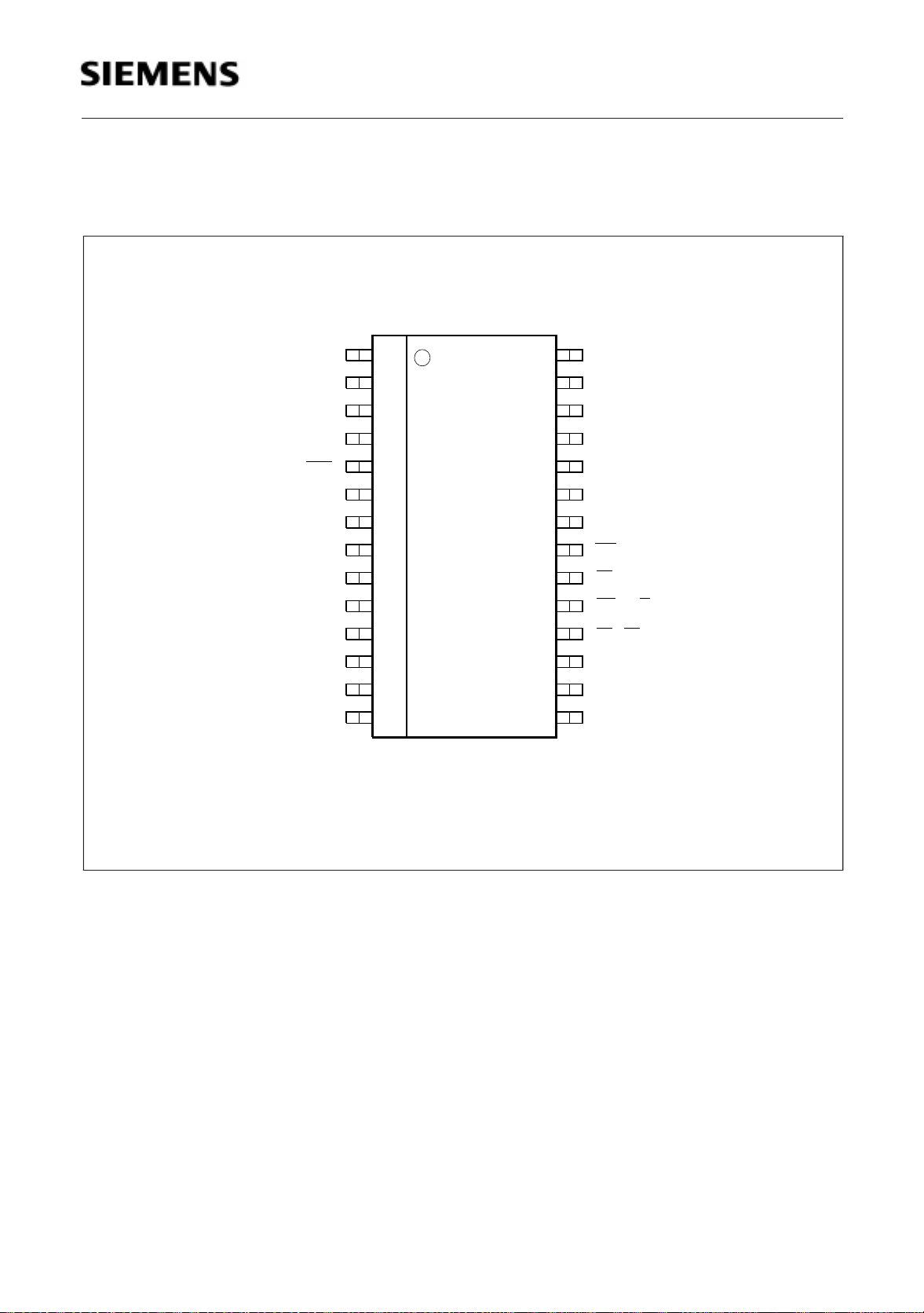
1.2 Pinning Diagram
(top view)
PEF 2015
Overview
V
DD
ALE, A0
RxD
TSC
TxD
PFS
PDC
AD0
AD1
AD2
AD3
AD4
AD5
1
2
3
4
5
6
7
8
9
10
11
12
13
14
MICO
28
27
26
25
24
23
22
21
20
19
18
17
16
15
MIC_PINN.DRW
RES
A3
A2A1
DD
DU
FSC
DCL
INT
CS
WR, R/W
RD, DS
AD7
AD6
V
SS
Figure 1 Pinning Diagra m
Semiconductor Group 8 12.97

1.3 Pin Description
PEF 2015
Overview
Pin
No.
23 FSC I/O Frame Synchronizati on
22 DCL I/O Data Clock
24 DU, SIP4 I, I/O (OD) Data Upstream, Input IOM- or PCM-configuration.
25 DD, SIP0 O, I/O (OD) Data Downstream, Output IOM- or PCM-configuration
Symbol Input (I)
Output (O)
Function
Input or output in IOM-c onfigur at ion.
Direction indication in SLD-mode.
Input or output in IOM-c onfigur at ion. Slave clock in
SLD mode.
Single or double data rate in IOM-configuration, single
data rate in SLD-mode.
Serial Interface Port, SLD configuration.
Serial Interface Port, SLD configuration.
Depending on the bit OMDR:COS this line has
push-pull or open drain characteristic.
For unused or unassigned channels or when bit
OMDR:CSB is reset the pin is in the state high
impedance.
7 PFS I PCM-Interface Frame Synchronization
8 PDC I PCM-Interface Data Clock
Single or double data rate.
6 TxD O Transmit PCM-Interface Data
Time-slot or ient ed dat a is shifted out of the MICOs
upstream data memor y on this line. For time-slots
which are flagged in the tristate dat a mem ory or
when bit OMDR:PSB is reset the pin is set in the
state high impedance.
5 TSC
4 RxD I Receive PCM- Inter face Data
O Tristate Control
Supplies a control signal for an external driver. This
line is ’low’ when corresponding TxD outputs are valid.
During reset this line is high.
Time-slot orient ed dat a is received on this p in and
forwarded into the downs tream data me mor y of the
MICO.
Semiconductor Group 9 12.97

PEF 2015
Overview
Pin
No.
9
10
11
12
13
14
16
17
2
3
26
27
Symbol Input (I)
Output (O)
AD0, D0
AD1, D1
AD2, D2
AD3, D3
AD4, D4
AD5, D5
AD6, D6
AD7, D7
A0/ALE
A1
A2
A3
I/O Address/Data Bus; multiplexed bus mode.
I Address Bus, demultiplexed mode.
Function
Transfers addresses from the µP to the MICO and data
between the µP and the MICO.
Data Bus; demultiplexed bus mode.
Transfers data between the µP and the MICO.
When driving data the pins have push pull
characteristic, otherwise they are in the state high
impedance.
Transfers addresses f rom the µP to the MICO.
Address Latch Enable, multiplexed mode.
ALE controls the on chip address latch in multiplexed
bus mode. While ALE is ’high’ the latch is transparent.
The falling edge latches the current address.
Note: During reset A0 and A1 are evaluated to
determ ine the bus mode.
18 R D, DS I Read, active low, Siem ens/ In tel bus mod e.
When ’low’ a read operation is indicated.
Data Strobe, Motoro la bus mode.
A rising edge marks the end of a read or write
operation.
19 W R
R/W
20 C S
,
I Write, active low, Siemens/ In tel bus mod e.
When ’low’ a write operation is indicated.
Read/Writ e, Motor ola bus mode .
When ’high’ a valid µP access identifies a read
operation, when ’low’ it identifies a write access.
I Chip Select, active ’low’.
A low on this line selects the MICO for a read/write
operation.
Semiconductor Group 10 12.97
PEF 2015
Overview
Pin
No.
Symbol Input (I)
Output (O)
Function
21 INT O (OD) Interrupt, active low.
This line is activated when the MICO requests an
interrup t. Due to the open dr ain (OD) charac teristic of
multiple interrupt sources can be connected
INT
together.
28 RES I Reset
A ’high’ forces the MICO into rese t state.
15 V
1V
SS
DD
I Ground (0 V)
I Supply Voltage (5 V +/- 5%)
Semiconductor Group 11 12.97
1.4 Logic Symbol
PEF 2015
Overview
FSC
DCL
DU
DD
DD
V
SS
V
MICO
PEF 2015
PFS
PDC
TxD
TSC
RxD
AD7..AD0
A3..A0
RD
(DS)WR(R/W)
CS
INT
RES
par_log1.drw
Figure 2 Logic Symbol
Semiconductor Group 12 12.97
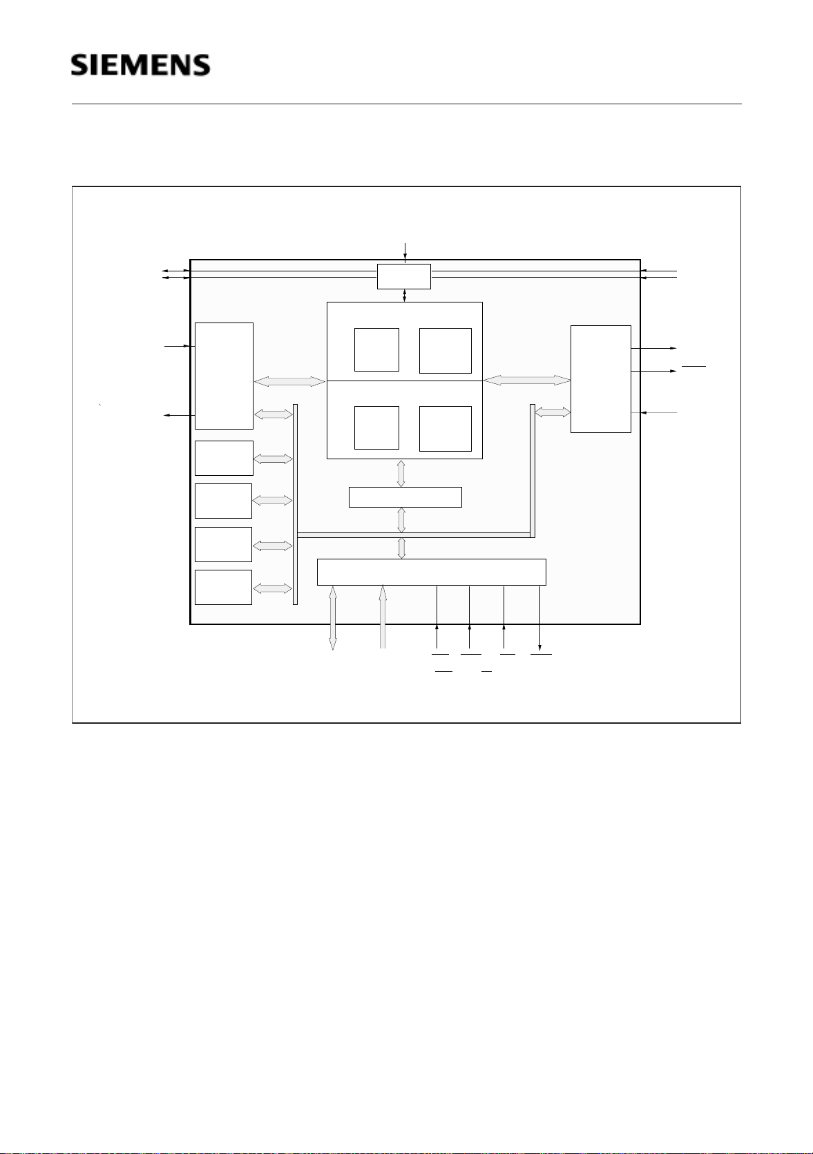
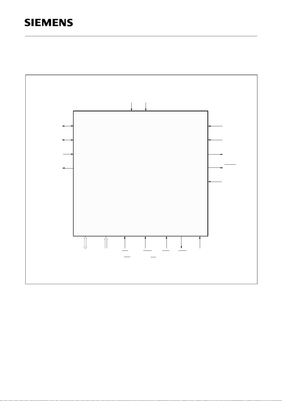
1.5 Functional Block Diagram
µP interface
DU
DD
MICO
TxD
RxD
PCM
Interface
upstream
(TRANSMIT)
downstream
(RECEIVE)
access c ont rol
Monitor
Sync.
Transfer
Timer
Timing
FSC
DCL
PFS
PDC
RES
TSC
mic_blk3.drw
AD7..AD0
A3..A0
DM
CM
DM
CM
CFI
Interfa ce
C/I
RD
(DS)WR(R/W)
CS
INT
PEF 2015
Overview
Figure 3 Functional Block Diagr am
Semiconductor Group 13 12.97
PEF 2015
Functional Description
2 Functional Description
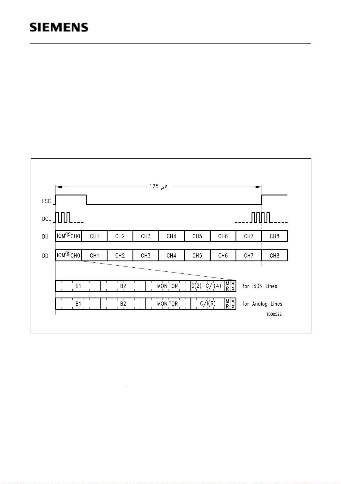
2.1 Configurable Interface CFI
The integrated CFI is a one port serial interface. It comprises two serial data lines
(upstream DU and downstream DD), a data clock input or output DCL and a frame sync
input or output FSC in IOM-applications. The clock frequency is either equ al to the data
rate or twice the data rate. The CFI can be conf igu red to data rat es up to 8.192 Mbit/s.
The CFI is typically used in IOM-2 or SLD configuration to connect layer-1 devices.
Figure 4 shows the IOM-2 Interface st ruc ture in Line Card Mode:
®
Figure 4 IOM
-2 Frame Structure with 2.04 8 Mbi t/s Data Ra te
2.2 Serial PCM Interface
The PCM int erface forma ts the dat a transmitted or received at the PCM-highways. It
consists of one port comprising a data receive (RxD), a data transmit (TxD) and an
output tristat e indication line (TS C
). The PCM interface is supplied with a frame signal
(PFS) and a PCM clock (PDC).
Data rates up to 8.192 Mbit/s are supported. To properly clock the PCM interface a PDC
signal with a frequency equal or twice the data rate has to be applied to the MICO.
Semiconductor Group 14 12.97
PEF 2015
Functional Description
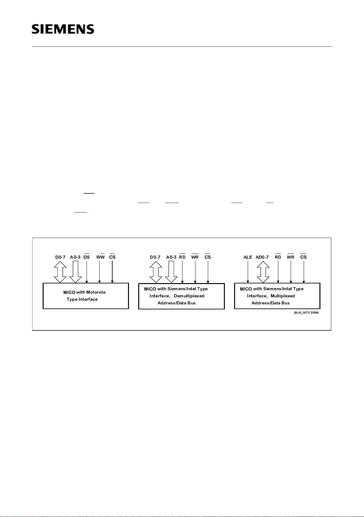
2.3 Microprocessor Int erf ace
The MICO supports Siemens/ I nte l and Motorola type microprocessor s. In the Siemens/
Intel type µP interface either a multiplexed or a demultiplexed bus structure may be
chosen.
The int erfac e type is sele cted by pulling up or down two address pins dur ing the reset
state (refer to Table 1, “Selection of Bus Interface,” on page 18). Pulling-up the
appropriate pins selects the Motor ola type µP interfac e, fixing them to ground c hooses
the Siemens/I ntel type µP interfac e mode. In case of a multiplexed Siemens/Intel bus
structure addr ess pin A0 takes over the ALE func tionality.
The microprocessor inter f ace consist s of the following lines:
• Data Bus, 8-bit wide, AD7..AD 0
• Address bus, 4-bit wide, A3.. A 0
• Chip select, CS
• Two read/write control lines: RD and WR (Intel mode) or DS and R/W (Motorola mode)
• Interr upt , INT
• Reset, RES
D0-7
MICO
DS
AR
0-3
with Motorola
Type Interface
/
W A
CS
0-7
D
MICO
Interface,
0-3
with Siemens/Intel Type
Demultiplexed MultiplexedInterface,
Address/Data Bus
RD
CS
0-7AD
ALEWR WR
with Siemens/Intel Type
MICO
Address/Data Bus
RD
CS
BUS_INTF.DRW
Figure 5 Selectabl e Bus Inte rfa ce Struct ures
2.4 Memory Struct ure and Sw itching
The memory block of the MICO perf orm s the switc hing functionality.
It consists of four sub blocks:
– Upstream data memory
– Downstream data mem ory
– Upstream control memory
– Downstream control memory.
The PCM-interface reads periodically from the upstream (writes periodically to the
downstream) data memory (cyclical access), see figure 6.
The CFI reads periodically the control memory and uses the extracted values as a
pointers to write to the upstream (read from the downstream) data memory (random
Semiconductor Group 15 12.97
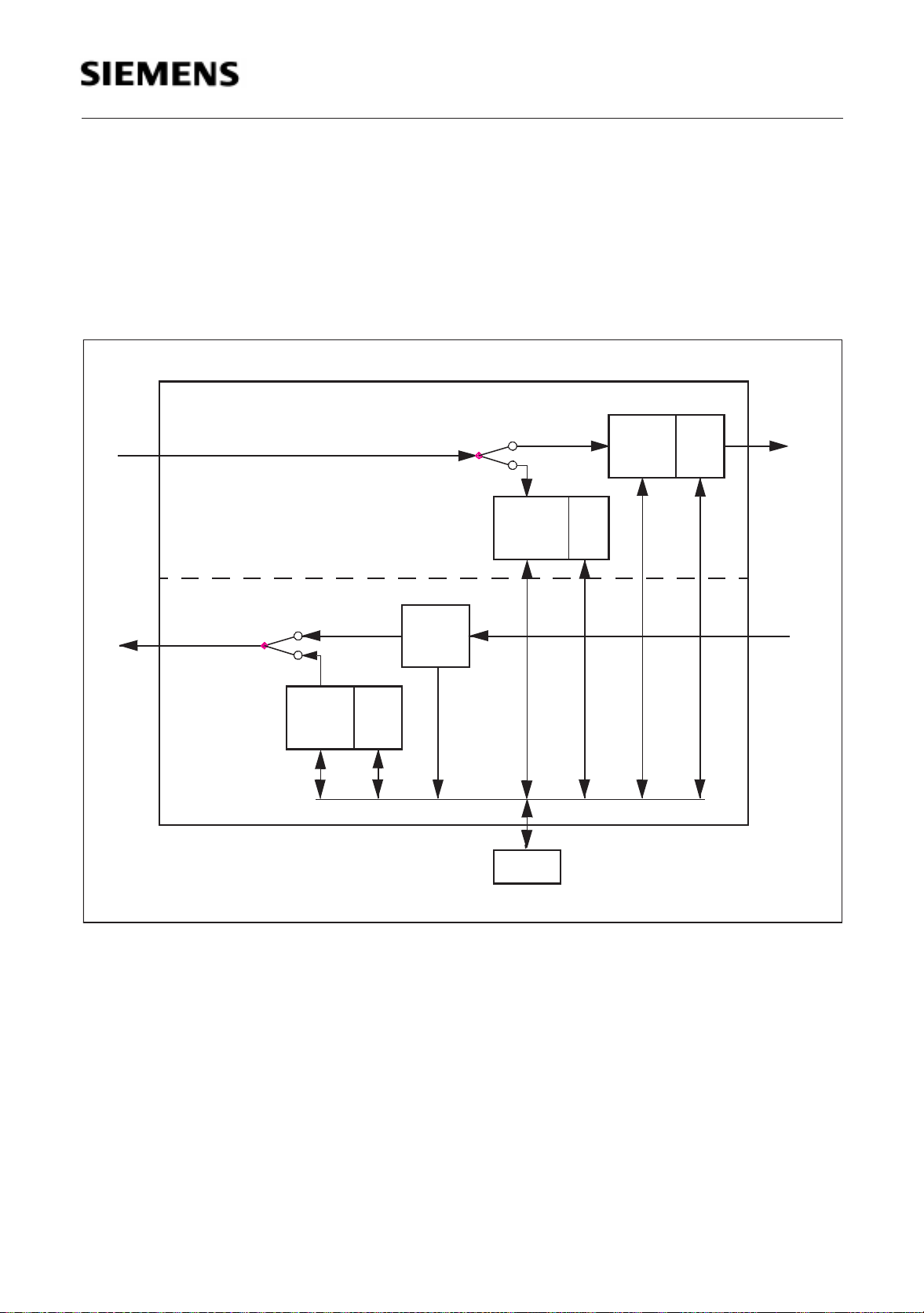
PEF 2015
Functional Description
access). In the case of C/I- or signaling channel applications the corr esponding data is
stored in the control memory. In order to select the application of choice, the control
memory pro vid es a code port io n.
The control memory is accessible via the µP-interface. In order to establish a connection
between CFI time slot A and PCM-interface t ime slot B, the B-pointer has to be loaded
into the control memor y location A.
DU
CFI
DD
Upstream
Downstream
Control
Memory
(CM)
DATA
Bits8
CODE
Bits4
Data Memory
DATA
Bits8
Control
Memory
(CM)
(DM)
DATA
8 Bits
CODE
4 Bits
Data Memory
DATA
Bits8
(DM)
CODE
Bits4
TxD
PCM
Rx D
µ P
Figure 6 MICO Memor y Struc ture
Semiconductor Group 16 12.97

PEF 2015
Functional Description
2.5 Pre-processed Channels , Layer-1 Support
The MICO supports the monitor/feature control and control/signaling channels according
to SLD- or IOM-2 interface prot ocol.
The monitor handler cont rols the data flow on the monitor/ feature contr ol channe l either
with or without active handshake protoco l. To reduce the dynamic load of the CPU a
16-byte transm it/ rece ive FIFO is provided.
The signaling handler supports different schemes (D-channel + C/I-channel, 6-bit
signaling, 8-bit signaling).
In downstream direction the relevant content of the control memory is transmitted in the
appropriate CFI time slot. In the case of centralized ISDN D-channel handling, a 16-kbit/
s D-channel received at the PCM-interface is included.
In upstream direct ion the signaling handler monitors the received dat a. Upon a change
it generates an interr upt, the channe l address is store d in the 9-byte deep C/I FIFO and
the actual value is store d in the cont rol memor y. In 6-bit a nd 8-bit signaling schem es a
double last look check is provided.
2.6 Special Functions
– Synchronous transfer.
This utility allows the synchr onous µP-ac cess t o two in depend ent c hannels o n the
PCM- or CFI-interface. Interrupts are generat ed to indicate the appropr iate access
windows.
– 7-bit hardware timer.
The MICO offers one hardware timer. It can be used to cyclically interrupt the CPU,
to determine the double last look period or to generate a proper CFI-multiframe
synchronization signal.
– Frame length checking.
The PFS-period is internally checked against the progr ammed f rame length.
Semiconductor Group 17 12.97

PEF 2015
Operational Description
3 Operational Descripti o n
The MICO, designed as a flexible line-card controller, has the following main
applications:
– Digital line cards, with the CFI typically configured as IOM-2, IOM-1 (MUX) or SLD.
– Analog line cards, with the CFI typically configured as IOM -2 or SLD.
– Intelligent NTs, where the MICO’s ability to configure the CFI as a PCM interface is
utilized.
To operate the MICO the user must be familiar with the device’s microprocessor
interface, interr upt structu re and res et logic.
The device is derived from the EPIC core. With some restrictions it is therefore
programmable like the EPIC.
3.1 Microprocessor Int erf ace O perat ion The MICO is programm ed via an 8-bit para llel interface that can be selected to be
(1) Motorola type, with control signals DS
(2) Siemens / Intel non-multiplexed bus type, with contro l signals WR
and CS
(3) Siemens / Intel multiplexed address/ dat a bus type , with control sign als
ALE, WR
The selection is performed via supplying address pins A0 and A1 during reset as follows:
Table 1 Selection of Bus Interface
A1, A0 during reset Bus Interface
11 Motorola type (1)
00 Siemens / Intel type, non-mu ltip lexed (2)
01 or 10 Siemens / Intel type, multiplexed (3)
.
, RD, and CS.
, R/W, and CS.
, RD ,
Pin A0 will take over the ALE functionality
Note: When selecting the multiplexed bus mode, it has to be ensured that during a MICO
device reset the A0/ALE p in receive s the appropr iate level and no AL E transf ers
µ
by the
C affect the interface type selection (refer also to figure 18, page 75).
When using the Siemens / Intel multiplexed interface, the MICO is addressed with even
addresses only (i.e. AD0 always 0), which allows data always to be transferred in the low
data byte. This simplifies the use of 16 bit Siemens / Intel type proce ssor s.
For a non-multiplexed bus structure the OMDR:RBS bit is needed in addition to the
address lines A3.. 0. OMDR:RBS (Register Bank Selec tion) selects one o f two register
banks.
Semiconductor Group 18 12.97

PEF 2015
Operational Description
RBS = ’1’ selects a set of registers used for device initialization (e.g. CFI and PCM
interface initializat ion).
RBS = ’0’ switches to a group of regist ers neces sary dur ing oper ation (e.g. con nection
programm ing).
The OMDR register containing the RBS bit can be accessed with either value of RBS.
Interrupts
An interrupt of the MICO is indicated by activating the INT
request can be determin ed by reading the ISTA register.
The INT
serviced. If a new status bit is set while an interrupt is being serviced, the INT
active. Howe ver, for the duration of a write access to the MASK- reg ister the INT
deactivated. When using an edge-triggered interrupt controller, it is t hus recommended
to rewrite the MASK-register at the end of any interr upt service routine.
Every interrupt source can be selectively masked by setting the respective bit of the
MASK-register. Such masked interrupts will not be indicated in the ISTA-register, nor will
they activate the INT
3.2 Clocking To operate properly , the MICO al ways requir es a PDC-cloc k.
To synchronize the PCM-side, the MICO should normally also be provided with a PFSstrobe. In most applications, the DCL and FSC will be output signals of the MICO,
derived from the PDC via presca lers.
If the required CFI-data rate cannot be derived from the PDC, DCL and FSC can also be
programmed as input signals. This is achieved by setting the MICO CMD1:CSS-bit.
Frequency and phase of DCL and FSC may then be chosen almost independently of the
frequency and phase of PDC and PFS. However, the CFI-clock source must still b e
synchronous to the PCM-interface clock source; i.e. the clock source for the CFIinterface and the clock source for the PCM-interface must be derived from the s ame
master clock.
-output is level active. It stays active until all interrupt sources have been
-line.
-line. The detailed cause of the
stays
-line is
3.3 Reset A reset pulse of at least 4 PDC clock cycles has to be applied at the RES pin. The reset
pulse sets all registers to their reset values descr ibe d in section 4.
The MICO is now in CM-r eset m ode ( refer to 4. 2.6. 7 ). As the hard ware reset does not
affect the MICO memories CM and DM, a ’software reset’ of the CM has to be performed.
Subsequently the MICO can be programmed to CM-in itialization, norma l operation or
test mode.
During reset the addr ess pins A0 and A1 are evaluate d to determine the bus inter face
type.
Semiconductor Group 19 12.97

PEF 2015
Operational Description
3.4 MICO Operation
The MICO is principally an intelligent switch of PCM-data between two serial interfaces,
the system interface (PCM-interface) and the configurable interface (CFI). Up to 128
channels per direction can be switched dynamically between the CFI and the PCMinterfaces. The MICO performs non-blocking space and time switching for these
channels which may have a bandwidth of 16, 32, 64 or 128 kbit/s on a per device basis.
Both interfaces can be programmed to operate at different data rates of up to 8.192 Mbit/
s. The PCM-interface consists of one duplex port with a tristate control signal. The
configurable interface can be selected to provide either one duplex port or two bidirectional (I/O) ports.
The configurable interface incor porat es a cont ro l block (layer-1 buffer) which allows the
µP to gain access to the cont rol chan nels of an IOM- (ISDN-O r ie nted Modu lar) or SLD(Subscriber Line Data) int erface. The MICO can handle the layer-1 f unctions b uffering
the C/I and monitor channels for IOM compatible devices and the featur e control and
signaling channels for SLD compatible devices. The layer-1 and codec devices are
connected to the CFI, which is then configured to operate as IOM-2, SLD or multiplexed
IOM-1 interface.
The configurable interface of the MICO can also be configured as plain PCM-interface
i.e. without IOM- or SLD-frame structure. Since it’s possible to operate the two seria l
interfaces at different data rates, the MICO can then be used to adapt two different PCMsystems.
The MICO can handle up to 8 ISDN-subscribers with their 2B+D channel structure or up
to 16 analog subscr ibers with their 1B channel structur e in IOM-configurat ion. In SLDconfiguration up to 4 analog subscribers can be accom mod ated .
The system interface is used for the connection to a PCM-back plane. On a typical digital
line card, the MICO switches the ISDN B-channels and, if required, also the D-channels
to the PCM-back plane. Due to its capability to dynamically switch the 16-kbit/s
D-channel, the MICO is one of the funda men tal bu ilding block s for net wo rks w ith either
central, decentral or mixe d signaling and packet data handling architecture.
3.4.1 PCM-Interface
The serial PCM-interface provides on e port consisting of a data transm it (TxD), a data
receive (RxD) and a tristate con trol (TS C
as the upstream direction, whereas the receive direction is referred to as the
downstream direction.
) line. The transmit direct ion is also refe rre d to
Data is transm itted and rec e ived a t norm al TTL /CM OS-levels, the ou tput d river s being
of the tristate type. Unassigned time slots may either be tristated, or programmed to
transmit a defined idle value. The selection of the states "high impedance" and "idle
value" can be per formed wit h a two bit reso lution. This tr istate c apability allows sever a l
devices to be connected together for concentrator functions. If the output driver
Semiconductor Group 20 12.97

PEF 2015
Operational Description
capability of the MICO should prove to be insufficient for a specific application, an
external driver contro lled by the TSC
The PCM-s tandby function makes it possible to switch all PCM-output lines to high
impedance with a single command. Internally, the device still works norm ally. Only the
output driver s a re s w itched off.
The number of time slots per 8-kHz frame is pro grammable in a wide range (from 4 to
128). In other words, the PCM-data rate can range between 256 kbit/s up to
8.192 Mbit/s. For time s lot encoding refer to figure 7.
The number of bits per frame is defined by the PCM-mode. There are three PCM-
modes.
The timing characteristics at the PCM-interface (data rate, bit shift, etc.) can be varied in
a wide range.
The PCM-interfac e has to be clocked with a PCM-Data Clock (PDC) signal having a
frequency equal to or twice the selected PCM-data rate. In single clock rate operation,
a frame consisting of 32 time slots, for example, requires a PDC of 2048 kHz. In double
clock rate operation, however, the same frame structure would require a PDC of
4096 kHz.
can be connected.
For the synchronizat ion of the time slot struct ure to an external PCM-syst em, a PCM-
Framing Signal (PFS) must be applied. The MICO evalua tes the rising PFS edge to
reset the int ernal time s lot count ers . In o rder to adap t the PFS-t im ing to diff er ent tim ing
requirements, the MICO can latch the PFS-signal with either the rising or the falling PDCedge. The PFS-signal defines the position of the first bit of the internal PCM-frame. The
actual position of the externa l upstream and downstream PC M-frames with respect to
the framing signal PFS can still be adjusted using the PCM-offset function of the MICO.
The offset can then be programmed such that PFS marks any bit number of the external
frame.
Furthermore it is possible to select either the rising or falling PDC-clock edge for
transmitting and sam p l ing the PCM-data .
Usually, the repetition rate of the applied framing pulse PFS is identical to the frame
period (125 µs). If this is the case, the loss of synchronism indicati on functio n can
be used to supervise the clock and framing signals for missing or additional clock cycles.
The MICO checks the PFS-period internally against the duration expected from the
programmed data rate. If, for example, double clock operation with 32 time slots per
frame is programm ed, the MICO expects 512 clock periods within one PFS-period. The
synchronous state is reached after the MICO has detected two consecutive correct
frames. The synchronous state is lost if one bad clock cycle is found. The
synchronization s tatus (gained or lost) can be read from an inter nal register and each
status change generates an interrup t.
Semiconductor Group 21 12.97
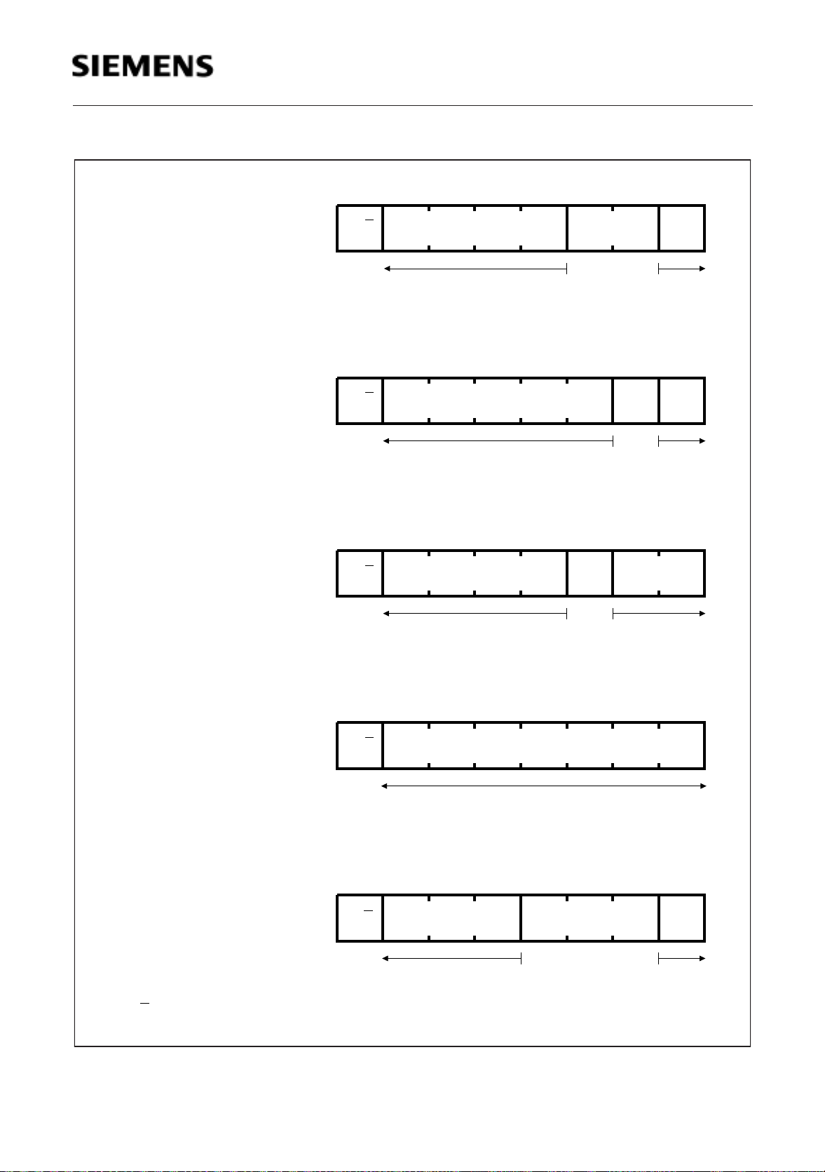
CFI Mode 0
PCM Mode 0
1 Duplex Port
32 Time-Slots
CFI Mode 1
1 Duplex Port
64 Time-Slots
U/D
U/D
PEF 2015
Operational Description
00
Time-Slot # (0-31)
0
Time-Slot # (0-63)
PCM Mode 1
1 Duplex Port
64 Time-Slots
CFI Mode 2
PCM Mode 2
1 Duplex Port
128 Time-Slots
CFI Mode 3
2 Bidirectional Ports
16 Time-Slots/Port
U/D
U/D
U/D
Time-Slot # (0-63)
Time-Slot # (0-127)
0
0
00
0
01
Time-Slot # (0-15)
U/D: Upstream (1) / Downstream (0)
ITD08063mod
Figure 7 Time Slot Encoding for the Diff erent PCM and CFI Modes
Semiconductor Group 22 12.97

PEF 2015
Operational Description
3.4.2 Configurable Interface
The serial configurable interface (CFI) can be operated either in duplex modes or in a bidirectional mode.
In duplex mode s the MICO provides one por t consisting of a data output (DD) and a
data input (DU) line. The output pin is called "Data Downstream" pin and the input pin is
called "Data Upstream" pin. These modes are especially suited to realize a standard
serial PCM-interface (PCM-h ighway) or to implement an IOM (ISDN-Oriented Mo dular)
interface. The IOM -interface gener at ed by t he M ICO o ffers all the f unction ality l ike C/ Iand monitor channel handling required for operating all kinds of IOM compatible layer-1
and codec devices.
In bi-directional mode the MICO provides two bi-directional ports (SIP). Each time slot
at any of these ports can individually be progra mmed as input or ou tput. This m ode is
mainly intended to realize an SLD-interface (Serial Line Data). In case of an SLDinterface the fr ame consists of eight time slots where the first four time slo ts serve as
outputs (downstream d irection) and the last four serv e as inputs (upstream d irection).
The SLD-interface gene rated by the M ICO offe rs signaling and featur e control cha nnel
handling.
Data is transmitted and received at normal TTL/CMOS-levels at the CFI. Tristate or
open-drain output drivers can be selected. In case of open-drain drivers, external pullup resistors are required. Unassigned output time slots may be switched to high
impedance or be programmed t o transmit a defined idle value. The selection between
the states "high impedanc e" or "idle value" can be perform ed on a per tim e slot basis.
The CFI-standby function switches all CFI-output lines to high impedance with a single
command. Internally the device still works normally, only the output drivers are switched
off.
The number of time slots per 8-kHz frame is programmable from 2 to 128. In other words,
the CFI-dat a rate can range betw een 128 kbit/s up to 8.192 Mbit/s . Since the MICO
offers one CFI-port the number of usable memory locations depends on the selected
data rate. In duplex modes port ’0’ has to be programmed, in bi-directional mode I/O port
’0’ and ’4’ have to be programmed. For deta ils refe r to figure 7.
The timing ch aracteristics at the CFI ( data rate, bit shift, etc .) can be var ied in a w ide
range.
The clock and fram ing signals necessary to operate the configurable inte rface may be
derived either fr om the clock and fr aming signals of the PCM-interfac e (PDC and PFS
pins), or may be fed in directly via the DCL- and FSC-pins.
In the first case, the CFI-data rate is obtained by internally dividing down the PCM-clock
signal PDC. Several presca ler fact ors are ava ilable to ob tain the most commo nly used
data rates. A CFI reference clock (CRCL) is generated out of the PDC-clock. The PCMframing signal PFS is used to synchronize the CFI-frame structure. Additionally, the
MICO generates clock and framing signals as outputs to operate the connected
Semiconductor Group 23 12.97
PEF 2015
Operational Description
subscriber circu its such as layer-1 and codec filter devices. The generated dat a clock
DCL has a frequency equal to or twice the CFI -dat a r ate. The gener ated framing s igna l
FSC can be chosen from a great variety of types to suit the different applications: IOM-2,
multipl exed IOM-1, SLD, etc.
Note that if PFS is selected as the framing signal source, the FSC-signal is an output
with a fixed timing relationship with respect to the CFI-data lines. The relationship
between FSC and the CFI-frame depends only on the select ed FSC-output wave for m
(CMD2-register). The CFI-offset function shifts both the frame and the FSC-output signal
with respect to the PFS-sign al.
In the second case, the CFI-data rate is derived from the DCL-clock, which is now used
as an input signal. The DCL-clock may also fir st be divided down by internal pres calers
before it serves as the CFI reference clock CRCL and before defining the CFI-data rate.
The framing signal FSC is used to synchronize the CFI- fram e struct ure.
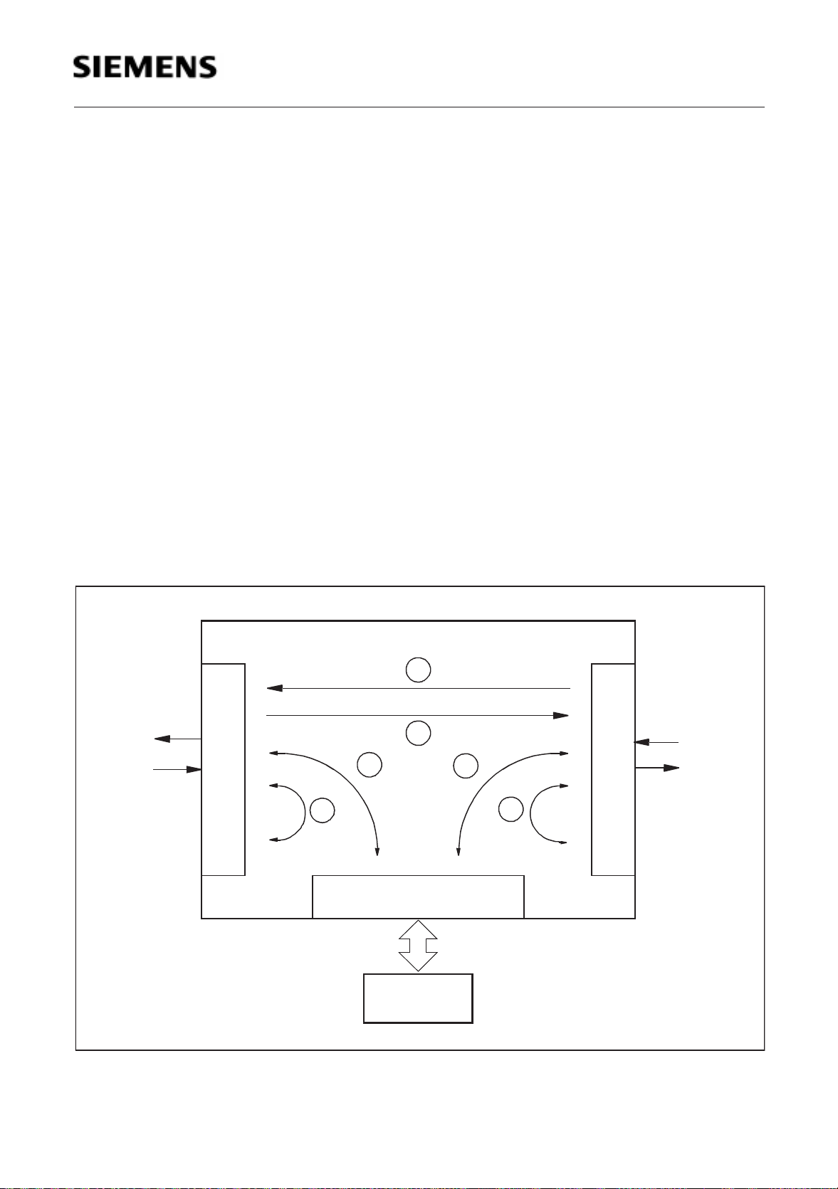
3.4.3 Switching Functi on s
The major tasks of the MICO is to dynamically switch PCM-data between the serial
PCM-interface, the ser ial con figurable interf ace (CFI) and the pa rallel µP- interfac e. All
possible switching paths are shown in figure 8.
MICO
1
2
CFI
34
56
PCM
µP Interface
µP
Figure 8 Switch ing Paths Inside the MICO
Semiconductor Group 24 12.97

PEF 2015
Operational Description
Note that the time s lot selections in upstream direction are completely independent of
the time slot selections in downstream direction.
CFI – PCM Time Slot Assignment
Switching paths 1 and 2 of figure 8 can be realized for a total number of up to 128
channels per path, i.e. up to 128 time slots in upstream and up to 128 time slots in
downstream direction. To establish a connection, the µP writes the addresses of the
involved CFI and PCM time slots to the control memory. The actual transfer is then
carried out frame by fram e wit hout further µP-intervention.
The switching pat hs 5 and 6 ca n be r ealized by pr ogramming time slot ass ignmen ts in
the control memory. The total number for such loops is limited to the number of available
time slots at the respective opposite interface, i.e. looping back a time slot from CFI to
CFI requires a spare upstream PCM time slot and looping back a time slot from PCM to
PCM requires a spare downstream and upstrea m CFI time s lot.
Time slot switching is always carried out on 8-bit time slots, the actual position and
number of transfer red bits can however be limited to 4-bit or 2-bit sub time slots with in
these 8-b it t im e slots. On t he CFI-side, o nly one sub time slot per 8-bit time slot c an be
switched, whereas on the PCM-interface up to 4 independent sub time slots can be
switched.
Examples are given in section 4 of the EPIC Application Manual 10.9 2.
Sub Time Slot Switchi ng
Sub time slot positions at the PCM-interface can be selected at random, i.e. each single
PCM time slot may cont ain any mix ture of 2- an d 4-bit sub t ime slots . A PCM tim e slot
may also contain more than one sub time slot. On the CFI however, two restrictions must
be observed:
– Each CFI time slot may contain one and only one sub time slot.
– The sub-slot position for a given bandwidth within the time slot is fixed on a per port
basis and therefor e on a per device basis.
For more deta iled information o n sub-channel switch ing please refer to chapt er 5.2 of
the EPIC-1 Application Manual 10.92.
µP-Transfer
Switching paths 3 and 4 of figure 8 can be realized for a ll available time slots. Path 3
can be implem ented by defining the corresp onding CFI time slots a s "µP-channels" or
as "pre-processed channels".
Each single time slot can individually be declared as "µP-channel". If this is the case,
the µP can write a static 8-bit value to a downstream time slot which is then transm itted
repeatedly in e ach fra me until a new value is loaded. In u pst ream direct ion, the µP can
read the received 8-bit value whenever required, no interrupt s being genera ted.
Semiconductor Group 25 12.97

PEF 2015
Operational Description
The "pre- processed channel " option must always be applied to two consecut ive time
slots. The first of these time slots must have an even time slot number . If two time- slots
are declared as "pre-processed channels", the first one can be accessed by the monitor/
feature control han dler, which gives access t o the fram e via a 16-byte FIFO . Although
this function is mainly intended for IOM- or SLD-applications, it could also be used to
transmit or receive a "burst" of data to or from a 64-kbit/s channel. The second preprocessed time slot, the odd one, is also accessed by the µP. In downstream direction a
4-, 6- or 8-bit static value can be tran smitted. In upstream direct ion the received 8-bit
value can be read. Additionally, a change detection mechanism will generate an interrupt
upon a change in any of the selected 4, 6 or 8 bits.
Pre-processed channels are usually programmed after Control Memory (CM) reset
during device initialization. Resetting the CM sets all CFI time slots to unassigned
channels (CM code '0000'). Of course, pre-processed channels can also be initialized or
re-initialized in the operational phase of the device.
To program a pair of pre-processed channels the correct code for the selected handling
scheme must be written to the CM. Figure 9 gives an overview of the available pre-
processing codes and their application. For further detail, please refer to chapter 5.5 of
the EPIC User’s Manual 02.97.
Semiconductor Group 26 12.97
 Loading...