

Siemens PEB2447H Datasheet

ICs for Communications
Memory Time Switch Extended Large
MTSXL
PEB 2447 Version 1.2
Data Sheet 03.97
T2447-XV12-D2-7600

PEB 2447
Revision History: Current Version: 03.97 (Editorial Update)
Previous Version: 01.95
Page
(in previous
Version)
Page
(in current
Version)
Subjects (major changes since last revision)
- 32 Register Address Arrangement (new)
Edition 03.97
This edition was realized using the software system FrameMaker
Published by Siemens AG,
Bereich Halbleiter, Marketing-
Kommunikation, Balanstraße 73,
81541 München
.
© Siemens AG 1997.
All Rights Reserved.
Attention please!
As far as patents or other rights of third parties are concerned, liability is only assumed for components, not for
applications, processes and c irc uit s imp lemented within componen ts or as s em blies.
The information describe s the t yp e of co m ponent and shall not be considered as assured characteristics .
Terms of delivery and rights to ch ange design reserved.
For questions on technology, delivery and prices please contact the Semiconductor Group Offices in Germany or
the Siemens Companies and R epresentatives worldwide (s ee address list).
Due to technical requireme nt s com ponents may contain dange rous substances. For informa tio n on t he t y pes in
question please contact yo ur nearest Siemens Office, Semic onductor Group.
Siemens AG is an approved CECC manufacturer.
Packing
Please use the recycling ope rat ors k now n t o y ou. W e ca n als o help you – get in touch with your neares t sa les
office. By agreement we will take packing material back, if it is sorted. You must bear the costs of transport.
For packing material that is returned to us unsorted or which we are not obliged to accept, we shall have to invoice
you for any costs incurred.
Components used in life-support devices or systems must be expressly authorized for such purpose!
Critical components
systems
1 A critical component is a component used in a life-support device or system whose failure can reasonably be
2 Life support devices or system s are int ended (a) to be implanted in the huma n body, or (b) to support and/or
2
with the express written approval of the Semiconductor Group of Siem ens AG.
expected to cause the failure of that life-support device or system, or to affect its safety or effectiveness of that
device or system.
maintain and sustain human life. If th ey fail, it is rea so nable to assume that the health of th e us er m ay be endangered.
1
of the Semiconductor Group of Siemens AG, may only be used in life-support devices or

PEB 2447
Table of Contents Page
1Overview . . . . . . . . . . . . . . . . . . . . . . . . . . . . . . . . . . . . . . . . . . . . . . . . . . . . .4
1.1 Features . . . . . . . . . . . . . . . . . . . . . . . . . . . . . . . . . . . . . . . . . . . . . . . . . . . . . .4
1.2 Logic Symbol . . . . . . . . . . . . . . . . . . . . . . . . . . . . . . . . . . . . . . . . . . . . . . . . . .5
1.3 General Device Overview . . . . . . . . . . . . . . . . . . . . . . . . . . . . . . . . . . . . . . . .5
1.4 Pin Configuration . . . . . . . . . . . . . . . . . . . . . . . . . . . . . . . . . . . . . . . . . . . . . . .6
1.5 Pin Definitions and Functions . . . . . . . . . . . . . . . . . . . . . . . . . . . . . . . . . . . . . .6
2 Functional Description . . . . . . . . . . . . . . . . . . . . . . . . . . . . . . . . . . . . . . . .11
2.1 General Operation . . . . . . . . . . . . . . . . . . . . . . . . . . . . . . . . . . . . . . . . . . . . .11
2.2 Special Functions . . . . . . . . . . . . . . . . . . . . . . . . . . . . . . . . . . . . . . . . . . . . . .13
2.2.1 Control Memory Reset . . . . . . . . . . . . . . . . . . . . . . . . . . . . . . . . . . . . . . . . . .13
2.2.2 Evaluate Frame Measurement Signal . . . . . . . . . . . . . . . . . . . . . . . . . . . . . .13
2.2.3 MTSXL Selftest . . . . . . . . . . . . . . . . . . . . . . . . . . . . . . . . . . . . . . . . . . . . . . .13
2.3 Boundary Scan and TAP Controller . . . . . . . . . . . . . . . . . . . . . . . . . . . . . . . .14
2.3.1 Boundary Scan . . . . . . . . . . . . . . . . . . . . . . . . . . . . . . . . . . . . . . . . . . . . . . . .14
2.3.2 TAP Controller . . . . . . . . . . . . . . . . . . . . . . . . . . . . . . . . . . . . . . . . . . . . . . . .18
2.3.3 Use of Built in Selftest via the Boundary Scan Interface . . . . . . . . . . . . . . . .19
2.3.4 IDCODE . . . . . . . . . . . . . . . . . . . . . . . . . . . . . . . . . . . . . . . . . . . . . . . . . . . . .22
3 Operational Description . . . . . . . . . . . . . . . . . . . . . . . . . . . . . . . . . . . . . . .23
3.1 Initialization Procedure . . . . . . . . . . . . . . . . . . . . . . . . . . . . . . . . . . . . . . . . . .23
3.2 Operation Mode . . . . . . . . . . . . . . . . . . . . . . . . . . . . . . . . . . . . . . . . . . . . . . .23
3.3 Indirect Access Registers . . . . . . . . . . . . . . . . . . . . . . . . . . . . . . . . . . . . . . . .23
3.4 Frame Evaluation . . . . . . . . . . . . . . . . . . . . . . . . . . . . . . . . . . . . . . . . . . . . . .24
3.5 Input Offset and Output Offset . . . . . . . . . . . . . . . . . . . . . . . . . . . . . . . . . . . .25
3.6 Frame Delay . . . . . . . . . . . . . . . . . . . . . . . . . . . . . . . . . . . . . . . . . . . . . . . . . .27
4 Detailed Register Description . . . . . . . . . . . . . . . . . . . . . . . . . . . . . . . . . . .32
4.1 Register Address Arrangement . . . . . . . . . . . . . . . . . . . . . . . . . . . . . . . . . . .32
4.2 Mode Register (MODR) . . . . . . . . . . . . . . . . . . . . . . . . . . . . . . . . . . . . . . . . .33
4.3 Command Register (CMDR) . . . . . . . . . . . . . . . . . . . . . . . . . . . . . . . . . . . . .34
4.4 Status Register (STAR) . . . . . . . . . . . . . . . . . . . . . . . . . . . . . . . . . . . . . . . . .35
4.5 Interrupt Status Register (ISTA) . . . . . . . . . . . . . . . . . . . . . . . . . . . . . . . . . . .36
4.6 Mask Register (MASK) . . . . . . . . . . . . . . . . . . . . . . . . . . . . . . . . . . . . . . . . . .37
4.7 Memory Access Address/Code Register High (MACH) . . . . . . . . . . . . . . . . .37
4.8 Memory Access Address Register Low (MAAL) . . . . . . . . . . . . . . . . . . . . . .38
4.9 Memory Read Data Register Low (MRDL) . . . . . . . . . . . . . . . . . . . . . . . . . .39
4.10 Memory Read Data Register High (MRDH) . . . . . . . . . . . . . . . . . . . . . . . . . .39
4.11 Memory Write Data Register Low (MWDL) . . . . . . . . . . . . . . . . . . . . . . . . . .39
4.12 Memory Write Data Register High (MWDH) . . . . . . . . . . . . . . . . . . . . . . . . .40
4.13 Input Clock Shift Register Bank ICSR (15:0) . . . . . . . . . . . . . . . . . . . . . . . . .41
4.14 Output Clock Shift Register (OSCR) . . . . . . . . . . . . . . . . . . . . . . . . . . . . . . .42
4.15 Test Register (TSTR) . . . . . . . . . . . . . . . . . . . . . . . . . . . . . . . . . . . . . . . . . . .42
4.16 Frame Evaluation Register Low (FERL) . . . . . . . . . . . . . . . . . . . . . . . . . . . .43
4.17 Frame Evaluation Register High (FERH) . . . . . . . . . . . . . . . . . . . . . . . . . . . .43
5 Electrical Characteristics . . . . . . . . . . . . . . . . . . . . . . . . . . . . . . . . . . . . . .44
6 Package Outlines . . . . . . . . . . . . . . . . . . . . . . . . . . . . . . . . . . . . . . . . . . . . .51
Semiconductor Group 3 03.97
Memory Time Switch Extended Large
PEB 2447
MTSXL
Version 1.2 CMOS IC
1Overview
1.1 Features
• Non blocking time/space switch for 4.096- or
8.192-Mbit/s PCM systems
• Device clock 16.384 MHz
• Switching of up to 2048 incoming PCM channels to
up to 2048 outgoing PCM channels
• 32 input and 32 output PCM lines
• Tristate function for further expansion and tandem operation
•µP read access to PCM data
• Programmable clock shift with half clock step resolution for input and output
• Individual line delay measurement for 6 additional inputs
• Individual input offset programmable for 16 PCM inputs
• Boundary scan (fully IEEE1149.1 compatible)
• Built-in selftest (also usable via boundary scan interface)
• 8-bit Intel type demultiplexed µP interface
• All registers accessible by direct addressing
• In-operation adjustment of bit sampling without bit errors
• Low power consumption
• Single 5 V power supply
P-MQFP-100-2
Type Ordering Code Package
PEB 2447 H Q67103-H6594 P-MQFP-100-2
Semiconductor Group 4 03.97
1.2 Logic Symbol
PEB 2447
Overview
Figure 1
Functional Symbol
1.3 General Device Overview
The Siemens Memory Time Switch Extended Large MTSXL (PEB 2447) is a capacity
expansion of the MTSL (PEB 2047 ). It is a mon olithic CMOS switching device capable
of connecting maximally 2048 PCM input time slots to 2048 output time slots. In order to
manage the problem of different lin e delays, six additional FS inpu ts can be used as
frame measurement inputs and 16 different in put offsets of PCM frames are allowed.
Thus a frame wander can be compensated by adjusting the input offset during operation.
A special circuitry guarantees that no bit error will occur, when reprogramming the input
offsets.
The MTSXL on chip con nection memory and dat a memory are access ed via the 8-bit
standard µP interface (Intel demultiplexed type).
A built-in selftest mechanism – also activated by the µP – ensures proper device
operation in the system.
The PEB 2447 is fabricated using the advanced CMOS technology from Siemens and is
mounted in a P-MQFP-100-2 package. Inputs and outputs are TTL compatible.
Semiconductor Group 5 03.97
1.4 Pin Configuration
(top view)
OUT0
INT
TDO
TMS
TDI
TCK
OUT2
OUT1
OUT4
OUT3
OUT6
OUT5
SS
OUT7
V
V
DD
OUT9
OUT8
OUT12
OUT11
OUT10
OUT15
OUT14
OUT13
OUT18
OUT17
OUT16
OUT21
OUT20
OUT19
PEB 2447
Overview
OUT22
IN0
IN1
IN2
IN3
IN4
IN5
IN6
IN7
IN8
IN9
IN10
IN11
IN12
IN13
IN14
IN15
IN16
IN17
IN18
IN19
Index
Marking
80 79 78 77 76 75 74 73 72 71 70 69 68 67 66 65 64 63 62 61 60 59 58 57 56 55 54 53 52 51
81
82
83
84
85
86
87
88
89
90
91
92
93
94
95
96
97
98
99
100
1
2345678910
IN21
IN20
IN22
IN23
IN24
IN25
IN26
IN27
IN29
IN28
11
PEB2447
12 13 14 15 16 17 18 19 20 2122 23 24 25 26 27 28 29 30
IN31
IN30
V
DD
V
SS
FS0
CLK
FS1
FS2
FS3
FS4
FS5
A4
A3
A2
A1
A0
CS
RES
WR
50
41
40
RD
OUT23
OUT2449
OUT2548
OUT2647
OUT2746
OUT2845
OUT2944
OUT3043
OUT3142
V
SS
V
DD
D039
D138
D237
D336
D435
D534
D633
D732
SP31
ITP09593
Figure 2
1.5 Pin Definitions and Functions
Pin No. Symbol Input (I)
Function
Output (O)
Tristate (T)
14
V
SS
I Ground (0 V)
41
67
13
V
DD
I Supply Voltage: 5 V + 5 %.
40
66
Semiconductor Group 6 03.97
1.5 Pin Definitions and Functions (cont’d)
PEB 2447
Overview
Pin No. Symbol Input (I)
Output (O)
Tristate (T)
81
82
83
84
85
86
87
88
89
90
91
92
93
94
95
96
97
98
99
100
1
2
3
4
5
6
7
8
9
10
11
12
IN0
IN1
IN2
IN3
IN4
IN5
IN6
IN7
IN8
IN9
IN10
IN11
IN12
IN13
IN14
IN15
IN16
IN17
IN18
IN19
IN20
IN21
IN22
IN23
IN24
IN25
IN26
IN27
IN28
IN29
IN30
IN31
I
I
I
I
I
I
I
I
I
I
I
I
I
I
I
I
I
I
I
I
I
I
I
I
I
I
I
I
I
I
I
I
Function
PCM Input Ports: Serial data is receiv ed at
standard TTL levels.
15 CLK I Clock: 16.384 MHz device cl ock.
Semiconductor Group 7 03.97
1.5 Pin Definitions and Functions (cont’d)
PEB 2447
Overview
Pin No. Symbol Input (I)
Function
Output (O)
Tristate (T)
16
17
18
19
20
21
26
25
24
23
22
27 CS
FS0
FS1
FS2
FS3
FS4
FS5
A0
A1
A2
A3
A4
I
I
Frame Measuring Inputs: These inputs are used
as frame evaluation inputs.
I
I
I
I
I
I
I
Address Bus Bit 0 to 4: These inputs interface to
the systems address bus to select an internal
register for a read or write access.
I
I
I Chip Select: (low active) A low level selects the
MTSXL for a register access operation.
28 RES I Reset: A high signal on this Input forces the MTSXL
into reset state.
29 WR
I Write: (low active) This signal indicates a write
operation.
30 RD
I Read: (low active) This signal indicates a read
operation.
31 SP I Synchronization Pulse: The MTSXL is
synchronized to the PCM system via this line.
39
38
37
36
35
34
33
32
D0
D1
D2
D3
D4
D5
D6
D7
I/O/T
I/O/T
I/O/T
I/O/T
I/O/T
I/O/T
I/O/T
I/O/T
Data Bus: These pins transfer data between the µP
and the MTSXL.
Semiconductor Group 8 03.97
1.5 Pin Definitions and Functions (cont’d)
PEB 2447
Overview
Pin No. Symbol Input (I)
Output (O)
Tristate (T)
75
74
73
72
71
70
69
68
65
64
63
62
61
60
59
58
57
56
55
54
53
52
51
50
49
48
47
46
45
44
43
42
OUT0
OUT1
OUT2
OUT3
OUT4
OUT5
OUT6
OUT7
OUT8
OUT9
OUT10
OUT11
OUT12
OUT13
OUT14
OUT15
OUT16
OUT17
OUT18
OUT19
OUT20
OUT21
OUT22
OUT23
OUT24
OUT25
OUT26
OUT27
OUT28
OUT29
OUT30
OUT31
O/T
O/T
O/T
O/T
O/T
O/T
O/T
O/T
O/T
O/T
O/T
O/T
O/T
O/T
O/T
O/T
O/T
O/T
O/T
O/T
O/T
O/T
O/T
O/T
O/T
O/T
O/T
O/T
O/T
O/T
O/T
O/T
Function
PCM Output Port: Serial data is sent by these
lines. These pins can be tristated.
76 INT
O
(Open Drain)
Interrupt Line: Active low.
Reset when reading ISTA
77 TDO O/T Test Data Output: In the appropriate TAP
controller state test data, an instruction or the
selftest result is shifted out via this line.
Semiconductor Group 9 03.97

1.5 Pin Definitions and Functions (cont’d)
PEB 2447
Overview
Pin No. Symbol Input (I)
Function
Output (O)
Tristate (T)
78 TMS I
(internal
pull-up)
79 TDI I
(internal
pull-up)
Test Mode Select: 0 -> 1 transitions on this pin are
required to step through the TAP controller state
machine.
Test Data Input: In the appropriate TAP controller
state te st da t a or an i n st ru c ti o n is s h if t e d in v ia th i s
line.
80 TCK I Test Clock: Single rate test data clock (6.25 MHz)
Semiconductor Group 10 03.97

PEB 2447
Functional Description
2 Functional Description
The MTSXL is a memory time switch device. Operating with a device clock of
16.384 MHz it can connect any of 2048 PCM input channels to any of 2048 output
channels.
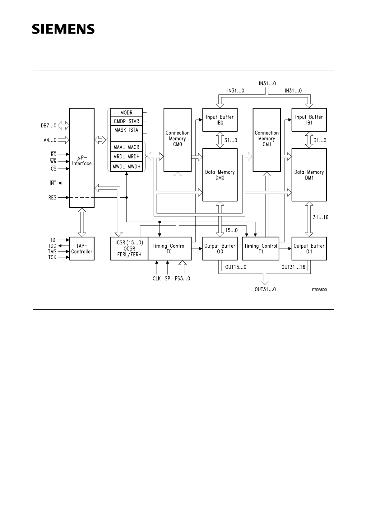
A general block diagram of the MTSXL is shown in figure 3.
2.1 General Operation
The input information of a complete frame is stored twice in the two on-chip 16-kbit data
memories DM 0 and DM 1 (Data Memory 0 and Data Memory 1). The incoming
2048 channels of 8 bits each are written in sequenc e into fixed po sitions of DM 0 and
DM 1. This is c ontrolled by the input counte r in the timing control bl ock with a 8 kHz
repetition rate.
For outputting, two connection memories (CM 0 and CM 1) are read in sequence
synchronously. Each entry in the conn ection memory CM 0 / CM 1 points to a lo cation
in data memory DM 0 / DM 1. The byte i n this data memory locat ion is transferred i nto
the current output time slot. The read access to the CM’s is controlled by an output
counter. CM 0 supplies the PCM data for outputs OU T0 to OUT15, CM 1 supplies the
PCM data for outputs OUT16 to OUT31.
Semiconductor Group 11 03.97
PEB 2447
Functional Description
Figure 3
Block Diagram of MTSXL
The synchronization of the input and output counters is achieved by a rising edge of the
sync pulse SP, which is always sampled with the falling edge of the device clock.
Different modes of operation are configurable at the PCM interfaces (see table 9).
Furthermore, 16 PCM input lines can be aligned with individual clock shift values to
compensate different line delays. If 32 inputs are used, one clock shift value controls two
ports at the same time.
Shifting of the output fram e is also possible, but all output lines are affe cted the same
way.
The input lines FS0 to FS5 are used as frame measurement inputs. After synchronizing
the device by the SP pulse the FS inpu ts can be evaluated on a per port basis. This
evaluation procedure is started by a microprocessor command. As a result the input
counter value on t he risin g edge of the FS sig nal ca n be re ad from an in ternal reg is ter.
Thus delay compensation is easily managed by programming appropriate clock shift
values and/or a possible software offset.
Semiconductor Group 12 03.97

PEB 2447
Functional Description
During operation of the chip a frame length check is also supplied, which controls correct
synchronization b y the SP pulse and ge nerates an i nterrupt in case of lo st or ac hieved
synchronizatio n.
The unused output ports are tristated by mode selection, whereas unused time slots are
tristated by an additiona l bit in the control memo ry. By using this tristate capability the
MTSXL can be easily expanded to a time switch of any size.
The standard 8-bit µP interface can communicate with Intel demultiplexed
microprocessors. It gi ves access to the internal registers a nd to the control and data
memory. All registers are directly addressable. The memories are accessed by a simple
four byte indirect access method.
2.2 Special Functions
The activity of all special functions can be read in the status register. Completion of these
functions is indicated by interrupts.
2.2.1 Control Memory Reset
Initialization of the device after a hardware reset (RES) is easily done with a µP
command “control memory reset”. After finishing this procedure all control memory
channels contain the information “tristated”. Apart from this tristate information the
contents of the C Memory is undefined.
2.2.2 Evaluate Frame Measurement Signal
A command including the address (0 … 5) will be given by the µP. The rising edge of the
corresponding frame measurement signal (FS0 … FS5) will be eval uated. The exact
timing of the FS ed ge can then be read from an internal 12-bit register (resolut ion of a
complete 8 kHz frame in half 16 MHz clock periods).
2.2.3 MTSXL Selftest
The switching path of th e M TSXL in clu din g in put buffer, data memory, control memory,
output buffer and timing control can be tes ted in the sys tem by a 2-ste p bui lt-in selfte st.
Activating this mechanism takes 2 × 0.6 25 ms (16.38 4 MHz ). Finally the res ult “selft est
ok/selftest not ok” can be read from the internal status register.
After test completion the control memo ry has a lso b een re set (conta ins t he inf ormat ion
tristated).
The selftest can also be started and checked via the boundary scan interface.
Note: For correct execution of the built-in selftest the MTSXL needs a value of
ICSR = 00. If MODR:PSB = 0 (e.g. after hardware reset) this value is programmed
automatically after start of the selftest procedure. If ICSR does not contain “00”
with MODR:PSB = 1 the selftest will fail.
Semiconductor Group 13 03.97
PEB 2447
Functional Description
2.3 Boundary Scan and TAP Controller
2.3.1 Boundary Scan
The MTSXL provides fully IEEE Std. 1149.1 compatible boundary scan support
consisting of
– a complete boundary scan
– a test access port controller (TAP controller)
– four dedicated pins (TCK, TMS, TDI, TDO)
– a 32 bit IDCODE register
All pins except power supply and ground are included in the boundary scan. Depending
on the pin functionality one, two or three boundary scan cells are provided:
Table 1
Boundary Scan Cell Type
Pin Type Number of Boundary Scan Cells Usage
Input 1 Input
Output 2 Output, enable
I/O 3 Input, output, enable
When the TAP controller is in the appropriate mode data is shifted into / out of the
boundary scan via the pins TDI / TDO using the 6.25 MHz clock on pin TCK.
The MTSXL pins are included in the boundary scan in the following sequence:
Table 2
Boundary Scan Sequence
Boundary Scan
Number TDI ->
Pin
Number
Pin
Name
Type Number of Scan
Cells
Default
Value
181IN0I10
282IN1I10
383IN2I11
484IN3I10
585IN4I10
686IN5I10
787IN6I10
888IN7I10
989IN8I10
10 90 IN9 I 1 0
11 91 IN10 I 1 0
Semiconductor Group 14 03.97
Table 2
Boundary Scan Sequence (cont’d)
PEB 2447
Functional Description
Boundary Scan
Number TDI ->
Pin
Number
Pin
Name
Type Number of Scan
Cells
12 92 IN11 I 1 0
13 93 IN12 I 1 0
14 94 IN13 I 1 0
15 95 IN14 I 1 1
16 96 IN15 I 1 0
17 97 IN16 I 1 0
18 98 IN17 I 1 1
19 99 IN18 I 1 0
20 100 IN19 I 1 1
21 1 IN20 I 1 0
22 2 IN21 I 1 0
23 3 IN22 I 1 0
24 4 IN23 I 1 0
25 5 IN24 I 1 1
Default
Value
26 6 IN25 I 1 0
27 7 IN26 I 1 0
28 8 IN27 I 1 0
29 9 IN28 I 1 0
30 10 IN29 I 1 0
31 11 IN30 I 1 1
32 12 IN31 I 1 1
33 15 CLK I 1 0
34 16 FS0 I 1 0
35 17 FS1 I 1 0
36 18 FS2 I 1 0
37 19 FS3 I 1 0
38 20 FS4 I 1 0
39 21 FS5 I 1 0
40 22 A4 I 1 0
41 23 A3 I 1 0
42 24 A2 I 1 0
Semiconductor Group 15 03.97
Table 2
Boundary Scan Sequence (cont’d)
PEB 2447
Functional Description
Boundary Scan
Number TDI ->
Pin
Number
Pin
Name
Type Number of Scan
Cells
Default
Value
43 25 A1 I 1 0
44 26 A0 I 1 0
45 27 CS I1 0
46 28 RES I 1 0
47 29 WR I1 0
48 30 RD
I1 0
49 31 SP I 1 0
50 32 AD7 IO 3 000
51 33 AD6 IO 3 000
52 34 AD5 IO 3 000
53 35 AD4 IO 3 000
54 36 AD3 IO 3 000
55 37 AD2 IO 3 000
56 38 AD1 IO 3 000
57 39 AD0 IO 3 000
58 42 OUT31 O 2 00
59 43 OUT30 O 2 00
60 44 OUT29 O 2 00
61 45 OUT28 O 2 00
62 46 OUT27 O 2 00
63 47 OUT26 O 2 00
64 48 OUT25 O 2 00
65 49 OUT24 O 2 00
66 50 OUT23 O 2 00
67 51 OUT22 O 2 00
68 52 OUT21 O 2 00
69 53 OUT20 O 2 00
70 54 OUT19 O 2 00
71 55 OUT18 O 2 00
72 56 OUT17 O 2 00
73 57 OUT16 O 2 00
Semiconductor Group 16 03.97
 Loading...