

Siemens PEB2245 Datasheet

ICs for Communications
Multipoint Switching and Conferencing Unit - Attenuation
MUSAC
PEB 2245 Version 1.2
Data Sheet 03.96
T2245-XV12-D1-7600

PEB 2245
Revision History: Current Version: 03.96
Previous Version: Digital Switching and Conferencing IC’s Data Book 01.94
Page (in
Version
01.94)
Page (in
current
Version)
Subjects (major changes since last revision)
163 8 Version 1.2
189 34 Figure 18 (Initializing the PEB 2245 for a 4096-kHz Device Clock)
corrected
201 46 Power supply current corrected
205 51 Timing corrected (
205 51 Timing added (
t
SPL min
t
= t
SH4 max
= 100 ns)
– 10 ns + t
CP4
CP4H
)
216 61 Conference number description corrected
– Appendix: Design sheets added
Edition 03.96
This edition was realized using the software system FrameMaker
Published by Siemens AG,
Bereich Halbleiter, Marketing-
Kommunikation, Balanstraße 73,
81541 München
©
Siemens AG 1996.
All Rights Reserved.
Attention please!
As far as patents or other rights of third parties are conc erned, liability is only assumed for components, not for app lic ations, processes
and circuits implemented within co mpo nent s or assemblies.
The information describes the type of component and shall not be considered as assured characteristics.
Terms of delivery and rights to change design reserved.
For questions on technology, delivery and prices please contact the Semiconductor Group Offices in Germany or the Siemens Companies
and Representatives worldwide (see address list).
Due to technical requirements components m ay contain dangerous substances. For information on the types in question please contact
your nearest Siemens Office, Sem iconductor Group.
Siemens AG is an approved CECC manufacturer.
Packing
Please use the recycling operators kno wn to you. We can also help you – get in touch with your near est sales office. By agreement we
will take packing material back, if it is sorted. You must bear the costs of transport.
For packing material that is returned to us unsorted or which we are not obliged to accept, we shall have to invoice you for any costs incurred.
Components used in life-support devices or systems must be expressly authorized for such purpose!
Critical components
written approval of the Semiconductor Group of Siemens AG.
1 A critical component is a component used in a life-support device or system whose failure can reasonably be expected to cause the
failure of that life-support device or system, or to affect its safet y or ef fectiv eness of that device or system.
2 Life support devices or systems are intended (a) to be implante d in the human body, or (b) to su pport and/o r maintain a nd sustain hu-
man life. If they fail, it is reasonable to assume that the health of the user may be endangered.
1
of the Semiconductor Group of Siemens AG, may only be used in life-support devices or systems2 with the express
.

PEB 2245
Table of Contents Page
1Overview . . . . . . . . . . . . . . . . . . . . . . . . . . . . . . . . . . . . . . . . . . . . . . . . . . . . .5
1.1 Features . . . . . . . . . . . . . . . . . . . . . . . . . . . . . . . . . . . . . . . . . . . . . . . . . . . . . .8
1.2 Pin Configuration
(top view) . . . . . . . . . . . . . . . . . . . . . . . . . . . . . . . . . . . . . . . . . . . . . . . . . . . . .9
1.3 Pin Definitions and Functions . . . . . . . . . . . . . . . . . . . . . . . . . . . . . . . . . . . . .10
1.4 Functional Symbols . . . . . . . . . . . . . . . . . . . . . . . . . . . . . . . . . . . . . . . . . . . .13
1.5 Device Overview . . . . . . . . . . . . . . . . . . . . . . . . . . . . . . . . . . . . . . . . . . . . . .14
1.6 System Integration . . . . . . . . . . . . . . . . . . . . . . . . . . . . . . . . . . . . . . . . . . . . .15
2 Functional Description . . . . . . . . . . . . . . . . . . . . . . . . . . . . . . . . . . . . . . . .19
2.1 Basic Functional Principles . . . . . . . . . . . . . . . . . . . . . . . . . . . . . . . . . . . . . .19
2.2 Microprocessor Interface and Registers . . . . . . . . . . . . . . . . . . . . . . . . . . . .29
3 Operational Description . . . . . . . . . . . . . . . . . . . . . . . . . . . . . . . . . . . . . . .33
3.1 Reset State . . . . . . . . . . . . . . . . . . . . . . . . . . . . . . . . . . . . . . . . . . . . . . . . . .33
3.2 Initialization Procedure . . . . . . . . . . . . . . . . . . . . . . . . . . . . . . . . . . . . . . . . . .33
3.3 Operation with a 4096-kHz Device Clock . . . . . . . . . . . . . . . . . . . . . . . . . . . .34
3.4 Standby Mode . . . . . . . . . . . . . . . . . . . . . . . . . . . . . . . . . . . . . . . . . . . . . . . .34
4 Detailed Register Description . . . . . . . . . . . . . . . . . . . . . . . . . . . . . . . . . . .35
4.1 Mode Register (MOD) . . . . . . . . . . . . . . . . . . . . . . . . . . . . . . . . . . . . . . . . . .35
4.2 Status Register (STA) . . . . . . . . . . . . . . . . . . . . . . . . . . . . . . . . . . . . . . . . . .39
4.3 Conference Status Register (CST) . . . . . . . . . . . . . . . . . . . . . . . . . . . . . . . .39
4.4 Conference Mask Register (CMR) . . . . . . . . . . . . . . . . . . . . . . . . . . . . . . . . .40
4.5 Indirect Access Register (IAR) . . . . . . . . . . . . . . . . . . . . . . . . . . . . . . . . . . . .40
4.6 Indirect Registers . . . . . . . . . . . . . . . . . . . . . . . . . . . . . . . . . . . . . . . . . . . . . .44
5 Electrical Characteristics . . . . . . . . . . . . . . . . . . . . . . . . . . . . . . . . . . . . . .46
5.1 Absolute Maximum Ratings . . . . . . . . . . . . . . . . . . . . . . . . . . . . . . . . . . . . . .46
5.2 DC Characteristics . . . . . . . . . . . . . . . . . . . . . . . . . . . . . . . . . . . . . . . . . . . . .46
5.3 Capacitances . . . . . . . . . . . . . . . . . . . . . . . . . . . . . . . . . . . . . . . . . . . . . . . . .46
5.4 AC Characteristics . . . . . . . . . . . . . . . . . . . . . . . . . . . . . . . . . . . . . . . . . . . . .47
5.5 Microprocessor Interface Timing . . . . . . . . . . . . . . . . . . . . . . . . . . . . . . . . . .49
5.5.1 Motorola Bus Mode . . . . . . . . . . . . . . . . . . . . . . . . . . . . . . . . . . . . . . . . . . . .49
TM
6 Conference Applications of the MUSAC
. . . . . . . . . . . . . . . . . . . . . . . .57
7 Package Outlines . . . . . . . . . . . . . . . . . . . . . . . . . . . . . . . . . . . . . . . . . . . . .65
Semiconductor Group 3

PEB 2245
Table of Contents Page
8 Appendix . . . . . . . . . . . . . . . . . . . . . . . . . . . . . . . . . . . . . . . . . . . . . . . . . . . .66
8.1 Initialization for Conferencing in a PBX . . . . . . . . . . . . . . . . . . . . . . . . . . . . .66
8.2 Programming a Conference in a PBX . . . . . . . . . . . . . . . . . . . . . . . . . . . . . .67
8.3 Programming Procedure for Switching TS’s . . . . . . . . . . . . . . . . . . . . . . . . .68
8.4 Programming Procedure for a PBX Conference . . . . . . . . . . . . . . . . . . . . . .69
IOM®, IOM®-1, IOM®-2, SICOFI®, SICOFI®-2, SICOFI®-4, SICOFI®-4µC, SLICOFI®, ARCOFI
ARCOFI
SICAT
MUSAC
Purchase of Siemens I
the I
®
-SP, EPIC®-1, EPIC®-S, ELIC®, IPAT®-2, ITAC®, ISAC®-S, ISAC®-S TE, ISAC®-P, ISAC®-P TE, IDEC®,
®
, OCTAT®-P, QUAT®-S are registered trademarks of Siemens AG.
™
-A, FALC™54, IWE™, SARE™, UTPT™, ASM™, ASP™ are trademarks of Siemens AG.
2
2
C-system provided the system confor ms to the I2C specifications defined by Philips. Copyright Philips 1983.
C components conveys a license under the Philips’ I2C patent to use the components in
®
, ARCOFI®-BA,
Semiconductor Group 4

PEB 2245
1 Overview
A Complete Family of Efficient Solutions
If the issue is digital switching and conferencing, the solution is flexibility, capacity, and economy.
Siemens Semiconductor offers the most economical answer to all conceivable applications in this
field. Our complete family of switching network devices satisfies even the most rigorous switching
demands.
A Complete Family of Efficient Solutions
Take our MTSC (Memory Time Switch CMOS) PEB 2045 with a switching capability of 512
incoming PCM channels to 256 outgoing PCM channels. It has the perfect size to economically
build medium sized switches. The design of a non-blocking switch for 5 12 PCM channels is possible
with a simple parallel configuration with a second MTSC.
If you need a non-blocking switch for up to 256 channels, we offer a smaller version of the MTSC,
the MTSS (Memory Time Switch Small) PEB 2046. And the MTSL (Memory Time Switch Large)
PEB 2047, the largest in our family, is capable of switching 1024 PCM channels.
Siemens also supplies the best solution for conferenc ing, ou r MUSAC (Multipoint Switching and
Conferencing Unit) PEB 2245 performs the complete switching functions of the MTSC, and offers
a signal processor for handling up to 64 conferencing channels in any combination. The input and
output channels can also be attenuated individually to achieve best transmission quality.
The MUSAC-A (Multipoint Switching and Conferencing Unit) PEB 2445 is an upward
compatible device to the MTSC and MUSAC. It offers in addition the attenuation and amplification
of every time slot.
Pin compatible device allow simplicity in hard ware and software design. To allow for more flexibility,
the PCM data rate can be 2, 4, or 8 Mbit/s – configurable also for mixed use.
Semiconductor Group 5
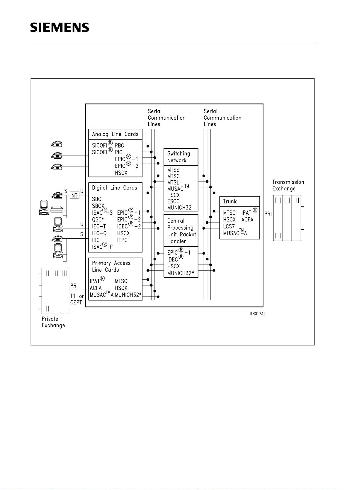
The figure below shows the general architecture of a digital exchange.
PEB 2245
Figure 1
General Exchange Architecture
System Background
Digital exchanges put calls through by newly arranging the speech signals coded with 8-bit words
(PCM time-slots). The code words are transmitted serially on PCM lines. The sampling frequency
of 8 kHz produces PCM frames with a duration of 125 µs. The transmission rate on the line
determines how many code words (speech channels) can be accommodated within a sampling
period. With a data rate of 2048 kbit/s for example, there are 32 time-slots of 8 bits each. 4 lines
with a data rate of 8192 kbit/s have a transmission capacity of 512 channels.
Semiconductor Group 6
PEB 2245
An overview on the complete switching and conferencing IC-family is shown in the following table:
Table 1
Complete Switching and Conferencing IC Family
MTSC
PEB 2045
Switching
capacity
(time-slots)
Input/output
lines
PCM-data rate
(Mbit/s)
Clock rate
(MHz)
Conferencing
Attenuation
PRI/T1 mode
Fractional T1
data bundling
µ
C access read read yes yes
Multipoint
switching
Power (mW)
max.
consumption
typ
Package
1)
in definition
512 × 256 256 × 256 1024 × 512 1024 × 1024 512 × 256 512 × 256 256 × 256 256 × 256
‘16/8 ‘8/8 ‘16/8 ‘16/8 ‘16/8 ‘16/8 ‘8/8
2/4/8 +
mixed mode
4.096
8.192
yes yes yes
50 50 100 170 100 100 50 50
P-DIP-40
P-LCC-44
MTSS
PEB 2046
2 2/4/8 +
4.096
8.192
P-DIP-40
P-LCC-44 P-LCC-44 P-LCC-44 P-LCC-44 P-LCC-44 P-LCC-44 P-LCC-44
MTSL
PEB 2047
mixed mode
4.096
8.192
yes yes 128-Kbit/s
MTSL 16
PEB 2047-16
2/4/8/16 +
mixed mode
4.096/8.192
16.384
MUSAC
PEB 2245
2/4/8 +
mixed mode
4.096
8.192
64 channels 64 channels
64 channels
3/6/9 dB
yes yes
MUSAC-A
PEB 2445
2/4/8 +
mixed mode
4.096
8.192
all channels
– 4 to 12 dB
EPIC-1
PEB 2055
SLD/IOM/
PCM
up to 8 up to 8
up to
8.192
channel
EPIC-S
PEB 2054
‘6/6
IOM/PCM
up to
8.192
128-Kbit/s
channel
Semiconductor Group 7 03.96
Multipoint Switching and
PEB 2245
Conferencing Unit
TM
(MUSAC
Preliminary Data CMOS IC
1.1 Features
Switching
● Time/space switch for 2048-, 4096- or 8192-kbit/s PCM
systems
● Switching of up to 512 incoming PCM-channels to up to
256 outgoing PCM channels
● 16 input and 8 output PCM lines
● Different kinds of modes (2048, 4096, 8192 kbit/s or mixed
mode)
● Configurable for primary access and standard applications
● Programmable clock shift with half clock step resolution for
input and output in primary access configuration
● Configurable for a 4096- and 8192-kHz device clock
● Tristate function for further expansion and tandem operation
● Tristate control signals for external drivers in primary access configuration
● 2048-kHz clock output in primary access configuration
● Space switch mode
)
P-LCC-44
Multipoint Switching
● Multiple independent LAN’s within one PBX
● Multiplexing of up to 64 channels
● 64-kbit/s channels
Type Version Ordering Code Package
PEB 2245 V1.2 Q67100-H6209 P-LCC-44 (SMD)
Semiconductor Group 8 03.96
PEB 2245
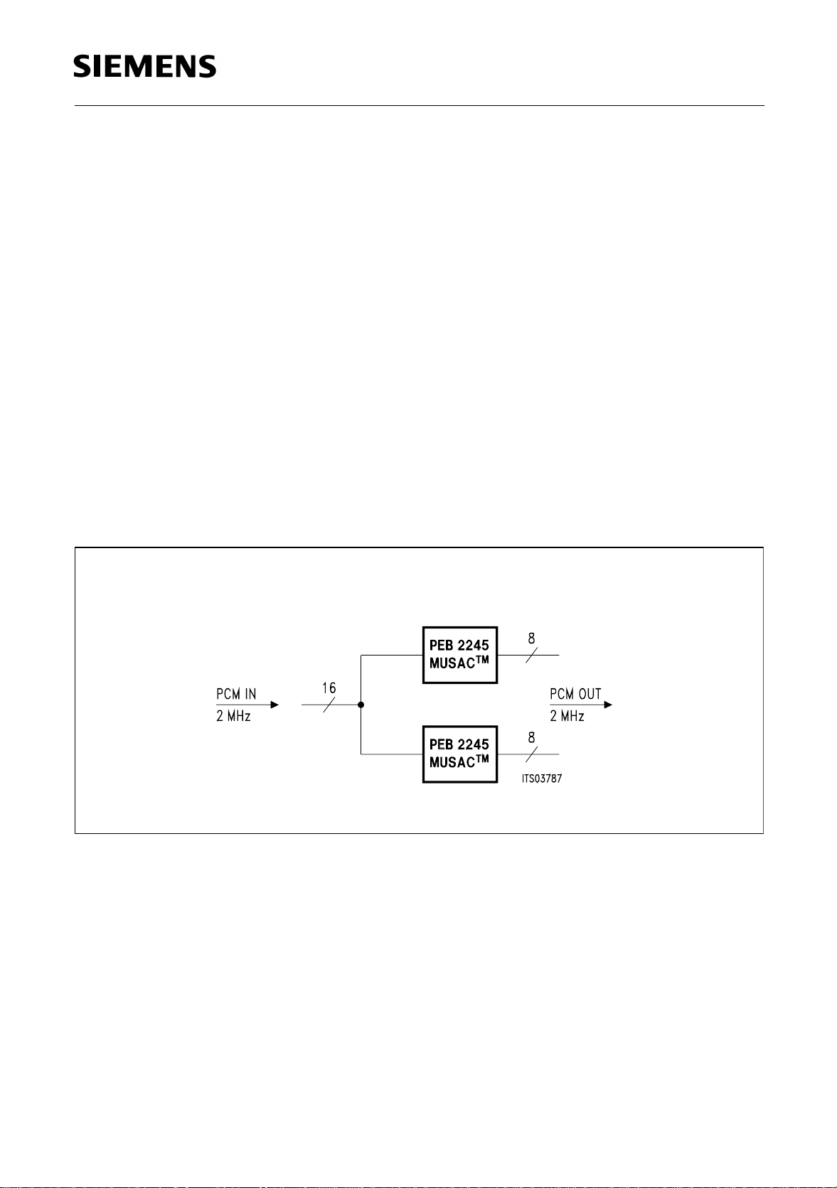
Conference Mode
● Up to 64 conference channels in any combination
● Up to 21 independent conferences simultaneously (3 subscribers)
● Programmable attenuation (0/3/6/9 dB) on each input channel
● Programmable attenuation (0/3 dB) on each output channel
● Programmable PCM-level adaption (attenuation or amplification) of up to 64 channels
● Programmable noise suppression (four thresholds)
● Conference overflow handling
● Tone insertion capability
● A-law / µ-law compatible
● Compatible with all kinds of PCM-byte formats
General
● 8-bit Motorola or Intel type µP interface
● Single + 5-V power supply
● Advanced low power CMOS technology
● TTL-compatible inputs/outputs
1.2 Pin Configuration
(top view)
Figure 2
Semiconductor Group 9
1.3 Pin Definitions and Functions
PEB 2245
Pin No. Symbol Input (I)
Function
Output (O)
1
6INT
V
SS
I Ground (0 V)
OD Interrupt Request: The signal is activated when a
conference overflow is detected. The microprocessor
may determine the specific conference in overflow by
reading the conference status register (CST). The
interrupt is maskable. INT
is an open drain output, thus a
“wired-or” combination of interrupt request outputs of
several MUSACs is possible. (A pull up resistor is
necessary).
3SP I Synchronization Pulse: The MUSAC is synchronized
relative to the PCM system via this line.
4
7
9
11
13
14
15
16
17
18
19
IN1
IN5
IN9
IN13
IN14
IN15
IN10
IN11
IN6
IN7
IN2
I
I
I
I
I
I
I
I
I
I
I
PCM-Input Ports: Serial data is received at these lines
at standard TTL levels.
5
8
10
12
IN0/TSC0
IN4/TSC1
IN8/TSC2
IN12/TSC3
I/O
I/O
I/O
I/O
PCM-Input Port / Tristate Control: In standard
configuration these pins are used as input lines, in
primary access configuration they supply control signals
for external devices.
20 IN3/DCL I/O PCM-Input Port / Data Clock: In standard configuration
IN3 is the PCM input line 3, in primary access
configuration it provides a 2048-kHz data clock for the
synchronous interface.
21
28
A0
A1
I
I
Address for Direct Register Access: These pins are
only active if a demultiplexed µP-interface mode is
selected.
22 CS
I Chip Select: A low level selects the MUSAC for a
register access operation.
23
V
DD
I Supply Voltage: 5 V ± 5 %.
Semiconductor Group 10
Pin Definitions and Functions (cont’d)
PEB 2245
Pin No. Symbol Input (I)
Function
Output (O)
24 RD
I Read: This signal indicates a read operation and is
internally sampled only if CS
is active. The MUSAC puts
data from the selected internal register on the data bus
with the falling edge of RD
. RD is active low (Siemens/
Intel bus mode).
DS
I Data Strobe: The rising edge marks the end of a valid
read or write operation (Motorola bus mode).
25 WR
I Write: This signal initiates a write operation. The WR
input is internally sampled only if CS
is active. In this
case the MUSAC loads an internal register with data
from the data bus at the rising edge of WR
. WR is active
low (Siemens/Intel bus mode).
R/W
I Read/Write: When “high”, identifies a valid µP access as
a read operation. When “low”, identifies a valid µP
access as a write operation (Motorola bus mode).
2ALEI Address Latch Enable: In the Intel type multiplexed µP-
interface mode a logical high on this line indicates an
address of an MUSAC internal register on the external
address/data bus. In the Intel type demultiplexed µPinterface mode this line is hardwired to
V
SS
, in the
demultiplexed Motorola type µP-interface mode it should
26
27
29
30
31
32
33
34
AD0
AD1
AD2
AD3
AD4
AD5
AD6
AD7
I/O
I/O
I/O
I/O
I/O
I/O
I/O
I/O
be connected to
Address Data Bus: If the multiplexed address/data µP-
interface bus mode is selected these pins transfer data
and addresses between the µP and the MUSAC.
If a demultiplexed mode is used, thes e bits interface with
the system data bus.
V
.
DD
35
36
37
38
40
41
42
43
OUT7
OUT6
OUT5
OUT4
OUT3
OUT2
OUT1
OUT0
O
O
O
O
O
O
O
O
PCM-Output Port: Serial data is sent by these lines at
standard CMOS- or TTL levels. These pins can be
tristated.
Semiconductor Group 11

Pin Definitions and Functions (cont’d)
PEB 2245
Pin No. Symbol Input (I)
Output (O)
39 RES I Reset: A high signal on this input forces the MUSAC into
44 CLK I Clock: 4096- or 8192-kHz device clock.
Function
reset state. The minimum pulse length is four clock
periods.
Semiconductor Group 12
1.4 Functional Symbols
PEB 2245
Figure 3
Functional Symbol for the Standard Configuration
Figure 4
Functional Symbol for the Primary Access Configuration
Semiconductor Group 13
PEB 2245
1.5 Device Overview
The Multipoint Switching and Conferenci ng Unit (MUSAC) combines a time switch unit (MTSC) and
a powerful signal processor on one chip. The MUSAC enhances the capabilities of a PBX by
supporting teleconferencing and multipoint data communication over voiceband channels. Digital
signal processing techniques are used to implement the conferencing algorithms. Up to 64
channels of the 512 incoming PCM channels may be manipulated by the signal processor and
output to any of 256 outgoing PCM channels. All functions are programmed and controlled via an
8-bit standard µP interface (Motorola or Intel type).
The MUSAC is fabricated using the advanced CMOS technology from Siemens and is mounted in
a P-LCC-44 package. Inputs and outputs are TTL-compatible.
Figure 5
Block Diagram of the PEB 2245
Semiconductor Group 14
PEB 2245
1.6 System Integration
Conferencing
The MUSAC is designed to connect any of the 512 PCM-input channels to any of 256 output
channels. Any input channel up to a total number of 64 can be handled in 21 independent
conferences simultaneously. Any conference com bination from 3 subscribers in 21 conferences up
to 64 subscribers in only one conference is possible. In order to ensure an acceptable speech
quality and to reduce echo and “singing” problems, the input channels can be attenuated
individually by 0, – 3 dB, – 6 dB or – 9 dB and the output channels by 0 or – 3 dB; additionally, input
signals below a threshold programmable to four different levels are disregarded.
To lessen the risk of instability in multiparty conferences the voice signal from every second channel
can be inverted so that disturbance signals in odd and even channels are subtracted from one
another.
If more capacity is needed, several devices can be connected. By connecting the 16 PCM-input
lines in parallel to two MUSACs, a nonblocking switching matrix for 512 subscribers can be
implemented: 128 input channels can be selected for up to 42 independent, simultaneous
conferences. Figure 6 shows such an arrangement. Due to the tristate capability of the MUSAC
larger switches with conferencing capability can be easily formed.
Figure 6
Memory Time Switch 16/16 for a Non-Blocking 512-Channel Switch with
Conferencing Capability
Semiconductor Group 15
PEB 2245
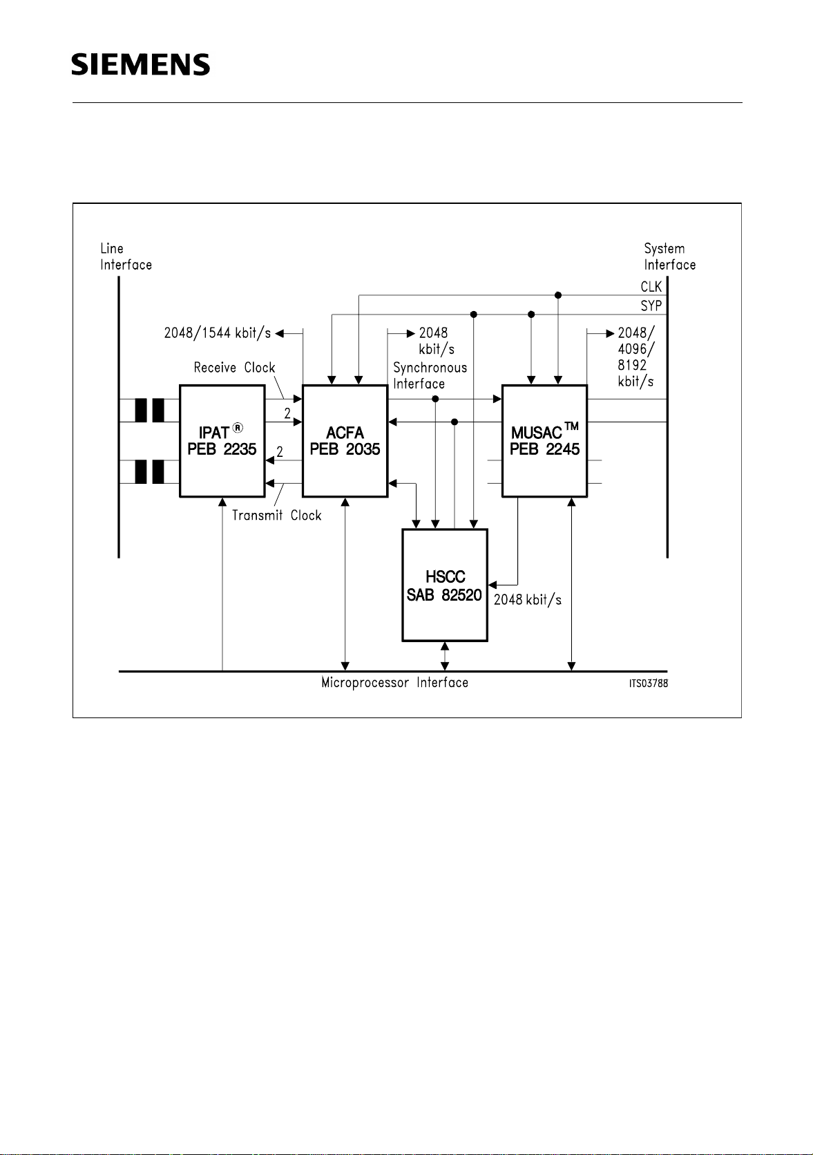
Figure 7 shows the architecture of a primary access board with common channel signaling using
four CMOS devices.
Figure 7
Architecture of a Primary Access Board
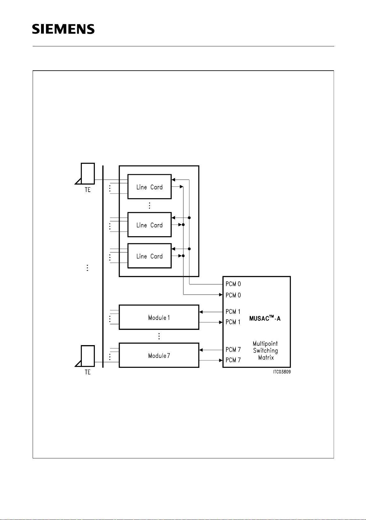
Multipoint Switching
In a multipoint configuration the communication between different stations is done by using a
common media. In a PBX system this can be achieved by connecting all stations to one (or more)
time-slots and transmitting the information back. Multipoint switching is a special form of
conferencing for data communication. In co ntrast to audio c onferences terminals broadcast data to
the MUSAC which are only “or-connected”. That is, at each bit time, the “conference sum” is “1” if
the input of one or more terminals is “1”; otherwise, the result is “0”. A simple example of such a
system using Siemens VLSI switching devices is shown in figure 8 .
ISDN subscribers are connected via line cards a nd PCM highways to a m ultipoint switc hing matrix .
The data from different terminals are summed up in the multipoint switching matrix and transmitte d
back to all stations. The switching matrix is build by using just one MUSAC. Every combination of
subscribers may be switched to the same transport m edia (time-slot), in this way enabling a num ber
of powerful multipoint communication systems.
Semiconductor Group 16
PEB 2245
Figure 8
Multipoint System Configuration for ISDN Subscribers
Semiconductor Group 17
PEB 2245
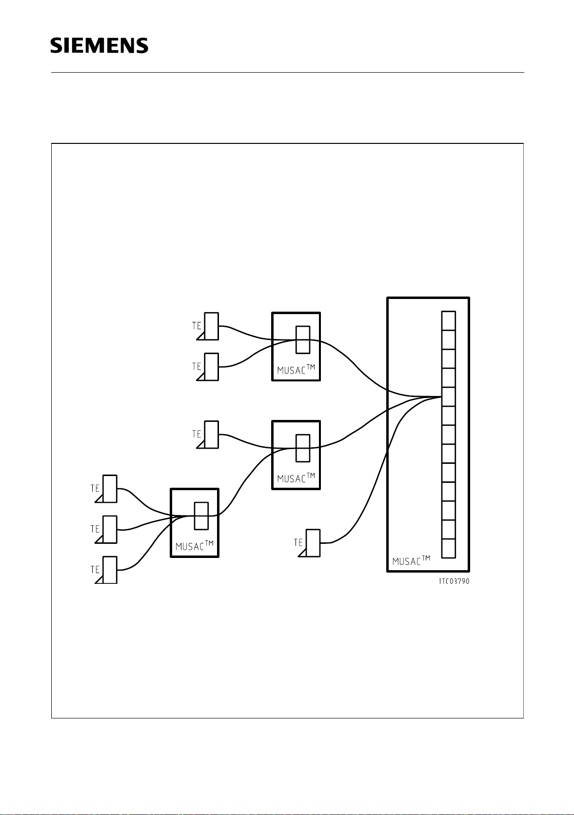
In order to establish a multipoint-connection with mo re than 64 terminals, yo u can form a multistage
arrangement, as shown in figure 9.
Figure 9
Multistage Arrangement
Semiconductor Group 18
2 Functional Description
PEB 2245
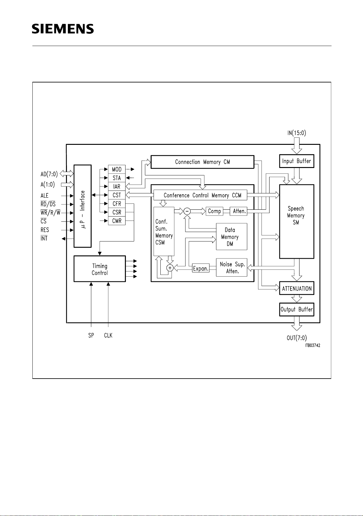
Figure 10
Detailed Block Diagram of the PEB 2245
2.1 Basic Functional Principles
The MUSAC is a memory time switch device for a PCM PBX sy stem, offering a va riety of additional
features like multipoint switching, conference calls, programmable noise suppression and
attenuation. The MUSAC works either in standard configuration for usual switching applications or
in the primary access configuration, where it realizes, together with the PEB 2035 (ACFA) and the
PEB 2235 (IPAT), the system interface for up to four primary multiplex access lines. In both
configurations the conference and multipoint switching capability can be used.
Semiconductor Group 19

PEB 2245
The block diagram is shown in figure 10 . The MUSAC is designed to c onnect any of 512 PCM-input
channels to any of 256 output channels. Any input channel up to a total number of 64 can be
handled in 21 independent conferences simultaneously. Any conference combination from 3
subscribers in 21 conferences up to 64 subscribers in only one conference is possible. Not more
than 8 subscribers should be connected to a single conference, however, in order to ensure an
acceptable speech quality. It can be improved by selecting an additional attenuation and acti vating
the noise suppression: The input channels can be attenuated by 0, – 3 dB, – 6 dB or – 9 dB and the
output channels by 0 or – 3 dB. Input signals below a threshold programmable to four different
levels are disregarded.
The input information of a compl ete frame is stored in the on-chip 4-Kbit Spee ch Memory (SM). The
incoming 512 channels of 8 bits each are written in sequence into fixed positions in the SM with a
repetition rate of 8 kHz. Additionally, in the second half of the frame the 64 conference output
channels of 8 bit each are written into the SM. The memory access is normally controlled by the
input counter in the timing control block when writing into the SM but by the conference unit when
writing the conference output channels . The read access is independent of the write access, so th at
both input and conference output channels can be read at any time.
For outputting, the Connection Memory (CM) is read in sequence. Each location in the CM points
to a location in the Speech Memory. The byte in t his SM location is read into the c urrent output timeslot. The read access of the CM is controlled by the output counter also contained in the timing
control block. In addition, in the first h alf of the frame the input channel s connecte d to a conference
are read in sequence by the Conference Unit (CU).
All connections are set up by an external controller which programs the Connection Memory (CM)
and the Conference Control Memory (CCM) using the microprocessor interface. The CM address
corresponds to one particular output time-slot and line number. The contents of this CM-location
points to a particular input time-slot and line number in the transparent mode. In the conference
mode or multipoint switching mode it contains the conference address and points to a conference
output location in the SM instead. The same conference address is used to access the CCM. The
parameters stored in the CCM include the input time-slot and line number, the associated
conference number as well as the noise suppression thresholds and the attenuation levels. The
conference number defines a unique locat ion in the Conferenc e Sum Memory (CSM) use d to store
the accumulated samples for each conference. The Conference Sum Memory is alternately loaded
in the first half of the frame and unloaded in the following second half. In the first half the input
samples are processed to implement the noise suppression, the expansion according to the
European A-law or the US µ-law and the attenuation function. The Data Memo ry (DM) buffers these
samples for output processing. The CSM is used to accumulate these samples and store the
resulting sum. During output processing the input s ample is retrieved from the Data Memo ry and the
appropriate sum from the Conference Sum Memory for subtraction, so that the channel output
signal contains the contribution of all the other channels in the conference except its own. After
output attenuation and PCM compression, the data are written in the Speech Memory for output
switching.
If one result of the subtractions exceeds the full scale value, a saturation appears and the MUSAC
signals this conference overflow condition by an interrupt. The conference number of the
conference in overflow is buffered in the Conference Status Register (CST) which can be retrieve d
by the external controller.
Semiconductor Group 20

PEB 2245
A tone to be inserted into a conference is h andled as an additional c onference subscriber usi ng any
input PCM channel (access to CCM) but without assigning an output time-slot (no access to CM).
Multipoint switching is a special form of conferencing for data communication. In the multipoint
switching mode several terminals are connected together. Normally only one should transmit at a
time; its signal is distribu ted to the oth er terminals . For colli sion detec tion purposes all inp ut signals
are summed up to construct the output si gnal. In cont rast to audio conferences term inals broadcas t
data to the MUSAC which are only “or-connected”. That is, at each bit time, the “conference sum”
is “1” if the input of one or more terminals is “1”; otherwise, the result is “0”. The data memory, the
subtractor, the linearization and attenuation are of no u se in this mode. The general procedure is the
same as for conferencing.
The chip architecture makes it possi ble to decrease the delay between incom ing and outgoing PCM
channels. The processed input samples are transmitted either in the same frame or in the next
frame at the latest.
Definitions
● The PEB 2245 works with either an 8192-kHz clock or a 4096-kHz clock. Henceforth, the
respective clock periods are referred to as
● The bits of a time-slot are numbered 0 through 7. Bit 0 (MSB) of a time-slot is the first bit to be
t
CP8
and t
CP4
.
received or transmitted by the MUSAC, bit 7 (LSB) the last.
Preparation of the Input Data (Input Buffer)
The PEB 2245 works in 2048-, 4096- or 8192-kbit/s PCM systems . The frame frequency is 800 0 Hz
in all 3 types of systems. Therefore a frame consists of 32, 64 or 128 time-slots of 1 byte each,
respectively. In order to fill the speech memory, which has a fixed capacity of 512 channels, either
16-, 8- or 4 input lines are necessary , respectively. Thus, in 4- and 8-MHz systems only some of the
16 input lines can be used.
Moreover, the PEB 2245 can also work with two different input data rates simultaneously. In this
case some of the PCM-input lines operate at one data rate, while others operate at another.
Table 2 states how many input lines are operating at the different data rates for all possible input
data rate combinations. In the fol lowing they will b e referred to as input m odes. The i nput mode th e
PEB 2245 is actually working in h as to be programm ed i nto the mode register, bits MI1, MI0, MO1,
MO0. In chapter 4.1 you will find a complete description which input line is connected to which
system, for each of the input modes.
Semiconductor Group 21
 Loading...