


ICs for Communications
Primary Rate Access Clock Generator and Transceiver
PRACT
PEB 22320
Version 2.1
Data Sheet 04.95

PEB 22320
Revision History Current Version: 04.95
Previous Version: 05.93
Page Subjects (changes since last revision)
10 Architecture of the PRACT
14 Input Jitter Specification
16 Jitter Attenuator Block Diagram
17 Clock- and Synchronization Table
18 Jitter Attenuation Characteristics
23 Master/Slave Selection
24 Reset
28 Delay Times
29 DC Characteristics
31 Recommended Oscillator Circuits
32, 33 Crystal Tuning Range
Data Classification
Maximum Ratings
Maximum ratings are absolute ratings; exceeding only one of these values may cause irreversible
damage to the integrated circuit.
Characteristics
The listed characteri stics are ensured over the operati ng range of the integrated circui t. Typical
characteristics specify mean val ues expected over the production spread. If not otherwise specified,
typical characteristics apply at
T
=25°C and the given supply voltage.
A
Operating Range
In the operating range the functions given in the circuit description are fulfilled.
For detailed technical information about “Processing Guidelines” and “Quality Assurance” for
ICs, see our Product Overview “ICs for Communications”

PEB 22320
General Information
Table of Contents Page
1 Features . . . . . . . . . . . . . . . . . . . . . . . . . . . . . . . . . . . . . . . . . . . . . . . . . . . . .5
1.1 Pin Configuration (top view) . . . . . . . . . . . . . . . . . . . . . . . . . . . . . . . . . . . . . . .7
1.2 Pin Definitions and Functions . . . . . . . . . . . . . . . . . . . . . . . . . . . . . . . . . . . . . .8
1.3 System Integration . . . . . . . . . . . . . . . . . . . . . . . . . . . . . . . . . . . . . . . . . . . . .10
2 Functional Description . . . . . . . . . . . . . . . . . . . . . . . . . . . . . . . . . . . . . . . .11
2.1 Receiver . . . . . . . . . . . . . . . . . . . . . . . . . . . . . . . . . . . . . . . . . . . . . . . . . . . . .12
2.1.1 Basic Functionality . . . . . . . . . . . . . . . . . . . . . . . . . . . . . . . . . . . . . . . . . . . . .12
2.1.2 Clock and Data Recovery . . . . . . . . . . . . . . . . . . . . . . . . . . . . . . . . . . . . . . .13
2.1.3 Input Jitter Tolerance . . . . . . . . . . . . . . . . . . . . . . . . . . . . . . . . . . . . . . . . . . .14
2.1.4 Jitter Attenuator and Clock Generator . . . . . . . . . . . . . . . . . . . . . . . . . . . . . .15
2.2 Transmitter . . . . . . . . . . . . . . . . . . . . . . . . . . . . . . . . . . . . . . . . . . . . . . . . . . .20
2.2.1 Basic Functionality . . . . . . . . . . . . . . . . . . . . . . . . . . . . . . . . . . . . . . . . . . . . .20
2.2.2 Output Jitter . . . . . . . . . . . . . . . . . . . . . . . . . . . . . . . . . . . . . . . . . . . . . . . . . .22
2.3 Local Loopback . . . . . . . . . . . . . . . . . . . . . . . . . . . . . . . . . . . . . . . . . . . . . . .22
2.4 Remote Loopback . . . . . . . . . . . . . . . . . . . . . . . . . . . . . . . . . . . . . . . . . . . . .22
2.5 Bypass Jitter Attenuator . . . . . . . . . . . . . . . . . . . . . . . . . . . . . . . . . . . . . . . . .22
2.6 Microprocessor Interface . . . . . . . . . . . . . . . . . . . . . . . . . . . . . . . . . . . . . . . .22
2.7 Receiver Loss of Signal Indication . . . . . . . . . . . . . . . . . . . . . . . . . . . . . . . . .22
2.8 Master/Slave Selection . . . . . . . . . . . . . . . . . . . . . . . . . . . . . . . . . . . . . . . . .23
3 Operational Description . . . . . . . . . . . . . . . . . . . . . . . . . . . . . . . . . . . . . . .24
3.1 Reset . . . . . . . . . . . . . . . . . . . . . . . . . . . . . . . . . . . . . . . . . . . . . . . . . . . . . . .24
3.1.1 Reset with CS Pin Fixed to V
. . . . . . . . . . . . . . . . . . . . . . . . . . . . . . . . . . .24
SS
3.1.2 Reset Using CS Pin to Latch Programming (a controller is used) . . . . . . . . .26
3.2 Operation . . . . . . . . . . . . . . . . . . . . . . . . . . . . . . . . . . . . . . . . . . . . . . . . . . . .27
4 Electrical Specification . . . . . . . . . . . . . . . . . . . . . . . . . . . . . . . . . . . . . . . .28
4.1 Absolute Maximum Ratings . . . . . . . . . . . . . . . . . . . . . . . . . . . . . . . . . . . . . .28
4.2 Delay Times . . . . . . . . . . . . . . . . . . . . . . . . . . . . . . . . . . . . . . . . . . . . . . . . . .28
4.2.1 Delay from XDIP/XDIN to XL1/XL2 . . . . . . . . . . . . . . . . . . . . . . . . . . . . . . . .28
4.2.2 Delay from RL1/RL2 to RDOP/RDON . . . . . . . . . . . . . . . . . . . . . . . . . . . . . .28
4.3 DC Characteristics . . . . . . . . . . . . . . . . . . . . . . . . . . . . . . . . . . . . . . . . . . . . .29
4.4 Characteristics . . . . . . . . . . . . . . . . . . . . . . . . . . . . . . . . . . . . . . . . . . . . . . . .30
4.5 Recommended Oscillator Circuits . . . . . . . . . . . . . . . . . . . . . . . . . . . . . . . . .31
4.6 AC Characteristics . . . . . . . . . . . . . . . . . . . . . . . . . . . . . . . . . . . . . . . . . . . . .34
4.6.1 Dual Rail Interface . . . . . . . . . . . . . . . . . . . . . . . . . . . . . . . . . . . . . . . . . . . . .34
4.6.2 System Clock Interface . . . . . . . . . . . . . . . . . . . . . . . . . . . . . . . . . . . . . . . . .36
4.6.3 Microprocessor Interface . . . . . . . . . . . . . . . . . . . . . . . . . . . . . . . . . . . . . . . .38
4.6.4 XTAL Timing . . . . . . . . . . . . . . . . . . . . . . . . . . . . . . . . . . . . . . . . . . . . . . . . .39
Semiconductor Group 3

PEB 22320
4.7 Pulse Templates - Transmitter . . . . . . . . . . . . . . . . . . . . . . . . . . . . . . . . . . . .40
4.8 Overvoltage Tolerance . . . . . . . . . . . . . . . . . . . . . . . . . . . . . . . . . . . . . . . . . .42
5 Package Outlines . . . . . . . . . . . . . . . . . . . . . . . . . . . . . . . . . . . . . . . . . . . . .45
IOM®, IOM®-1, IOM®-2, SICOFI®, SICOFI®-2, SICOFI®-4, SICOFI®-4µC, SLICOFI®, ARCOFI
ARCOFI
SICAT
MUSAC
Purchase of Siemens I
the I
®
-SP, EPIC®-1, EPIC®-S, ELIC®, IPAT®-2, ITAC®, ISAC®-S, ISAC®-S TE, ISAC®-P, ISAC®-P TE, IDEC®,
®
, OCTAT®-P, QUAT®-S are registered trademarks of Siemens AG.
™
-A, FALC™54, IWE™, SARE™, UTPT™, ASM™, ASP™ are trademarks of Siemens AG.
2
2
C-system provided the system confor ms to the I2C specifications defined by Philips. Copyright Philips 1983.
C components conveys a license under the Philips’ I2C patent to use the components in
®
, ARCOFI®-BA,
Semiconductor Group 4
Primary Rate Access Clock Generator
PEB 22320
and Transceiver
PRACT
Preliminary Data CMOS
1 Features
• ISDN line interface for 1544 and 2048 kbit/s (T1 and
CEPT)
• Data and clock recovery
• Transparent to ternary codes
• Low transmitter output impedance for a high return
loss with reasonable protection resistors (CCITT
G.703 requirements for the line input return loss
fulfilled)
• Adaptively controlled receiver threshold
• Programmable pulse shape for T1 applications
• Jitter specifications of CCITT I.431 and BELLCORE
TR-NWT-000499 publications met
• Wander and jitter attenuation
• Jitter tolerance of receiver: 0.5 UI s
• Implements local and remote loops for diagnostic purposes
• Monolithic line driver for a minimum of external components
• Low power, reliable CMOS technology
• Loss of signal indication for receiver
• Clock generator for system clocks
P-LCC-44
Type Ordering Code Package
PEB 22320 N Q67100-A6059 P-LCC-44 (SMD)
The Primary Rate Access Clock Generator and Transceiver PRACT (PEB 22320) is a
monolithic CMOS device which implements the analog receive and transmit line
interface functions to primary rate PCM carriers. It may be programmed or hard wired to
operate in 1.544-Mbit/s (T1) or 2.048-Mbit/s (CEPT) carrier systems.
The PRACT recovers clock and data u sing an ada ptively con trolled receiv er thresho ld.
It will meet the requirement of CCITT I.431 and Bellcore TR-NWT-000499 Issue 5,
December 1993 (Transport System Generic Requirements) in case of pulse shape, jitter
tolerance and jitter transfer characteristic.
Semiconductor Group 5 04.95

PEB 22320
Features
Specially designed line interface circuits simplify the tedious task of protecting the device
against overvoltage damage while still meeting the return loss requirements.
The PRACT is suitable for use in a wide range of voice and data applications such as for
connections of digital switches and PBX’s to host computers, for implementations of
primary ISDN subscriber loops as well as for terminal applications. The maximum range
is determined by the maximum allowable attenuation.
In the T1 case the PRACT’s power consumption is mainly determined by the line length
and type of the cable.
Semiconductor Group 6
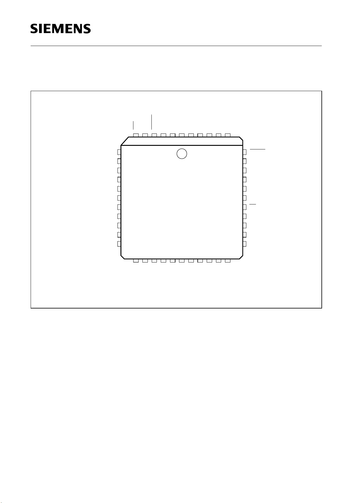
1.1 Pin Configuration
(top view)
PEB 22320
Features
FSC
LS0
XTAL4
LS1
XTAL2
XTAL1
LS2
CLK16M
CLK12M
SYNC
DD2
FSC
CLK4M
CLK4M
LL
RL2
V
RL1
JATT
6 5 4 3 2 1 44 43 42 41 40
8
9
10
11
12
PRACT
PEB 22320
13
14
15
16
17
SSX
DDX
V
DDX
V
XL1
N.C.
SSX
V
XL2
V
N.C.
DDRVSSR
V
RL
MODE
CLK2M
2827262524232221201918
XTIN
397
38
37
36
35
34
33
32
31
30
29
CLK2M
RCLK
RDON
RDOPXTAL3
V
SSD
V
DDD
CS
XCLK
XDIP
XDIN
XTIP
ITP04874
Semiconductor Group 7

1.2 Pin Definitions and Functions
Pin Definitions and Functions
PEB 22320
Features
Pin No. Symbol Input (I)
Function
Output (O)
1
V
DD2
O Reference voltage for tapping the input transformer
2 RL2 I Line receiver pin 2
3 LL I Local loopback:
A high level selects the device for the local
loopback mode.
4
5
6
7
CLK4M
CLK4MOO
FSC
FSC
O
O
System clock 4.096 MHz inverted and
non-inverted
8-kHz frame synchronization pulse inverted and
non-inverted
8 LS0 I Line length select
9
10
XTAL4
XTAL3
O
I
Crystal connection 12.352 MHz
If an external clock generator is used and T1 mode
is selected the PRACT works as a master.
11 LS1 I Line length select
12
13
XTAL2
XTAL1
O
I
Crystal connection 16.384 MHz
When an external clock is used, normally if the
MODE pin is set high, the PRACT functions as a
master.
14 LS2 I Line length select
15 CLK16M O System clock 16.384 MHz
16 CLK12M O System clock 12.352 MHz
17 SYNC I If a clock is detected at the SYNC pin the PRACT
synchronizes to this clock (2.048 MHz for CEPT,
1.544 MHz for T1). (Please refer to table 3).
18, 19
V
DDX
I Positive power supply for transmit subcircuits
20 XL1 O Line transmit pin 1
21, 25 N.C. not connected
22, 23
V
SSX
I Ground for transmit subcircuits
24 XL2 O Line transmit pin 2
Semiconductor Group 8

Pin Definitions and Functions (cont’d)
PEB 22320
Features
Pin No. Symbol Input (I)
Function
Output (O)
26 RL I Remote loopback:
High level puts the device to the remote loopback
mode.
27 MODE I Master/Slave selection
If the MODE pin is set to a low level the PRACT
functions as a slave. (Please refer to table 3)
28
29
30
31
XTIN
XTIP
XDIN
XDIP
I
I
I
I
Positive and negative test data inputs, active low,
full bauded
Positive and negative data inputs, active low, full
bauded
32 XCLK I/O If the T1 mode is selected the XCLK is a clock
output with a clock frequency of 1.544 MHz.
Otherwise the XCLK is a clock input whose
frequency is 2.048 MHz. (Please refer to table 3)
33 CS
IChip Select:
A low level selects the PEB 22320 for a register
write operation.
34
35
36
37
V
DDD
V
SSD
RDOP
RDON
I Positive power supply for the digital subcircuits.
I Power ground supply for digital subcircuits.
O
O
Receive data output positive and negative, fully
bauded, active low.
38 RCLK O Receive clock refer to table 3.
39
40
41
42
CLK2M
CLK2MOO
V
V
SSR
DDR
I Power ground supply for receive subcircuits.
I Positive power supply for the receive subcircuits.
System clock 2.048 MHz inverted and
non-inverted.
43 JATT I If the JATT pin is set to a low level the jitter
attenuator is bypassed.
44 RL1 I Line receiver pin 1.
Semiconductor Group 9
PEB 22320
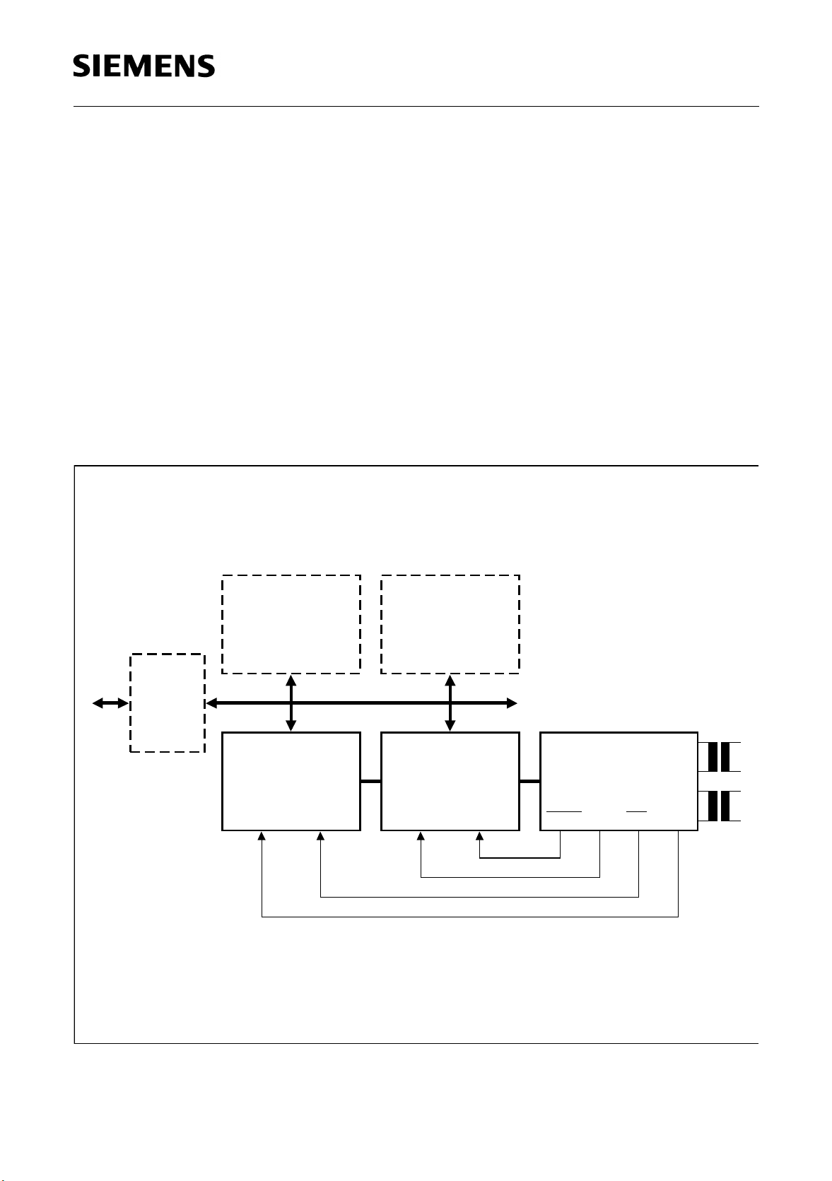
Features
1.3 System Integration Figure 1 shows the architecture of a primary access board for data transmission. It
exhibits the following functions:
– Line Interface (PEB 22320, PRACT)
– Clock and Data Recovery (PEB 22320, PRACT)
– Jitter Attenuation (PEB 22320, PRACT)
– Clock Generation (PEB 22320, PRACT)
– Coding/Decoding (PEB 2035, ACFA)
– Framing (PEB 2035, ACFA)
– Elastic Buffer (PEB 2035, ACFA)
– Multichannel Protocol Controller (PEB 20320, MUNICH32)
– System Adaptation (PEB 20320, MUNICH32)
– µP Interface (all devices)
PC
Interface
MUNICH32
PEB 20320
TCLK/RCLK TSP/RSP
kHz8
MHz2.048
MemoryMPU
ACFA
PEB 2035
SCLKSYPQ
8 kHz
PRACT
PEB 22320
CLK4M FSC FSC CLK2M
4.096 MHz
ITS04875
Figure 1
Architecture of the PRACT
Semiconductor Group 10
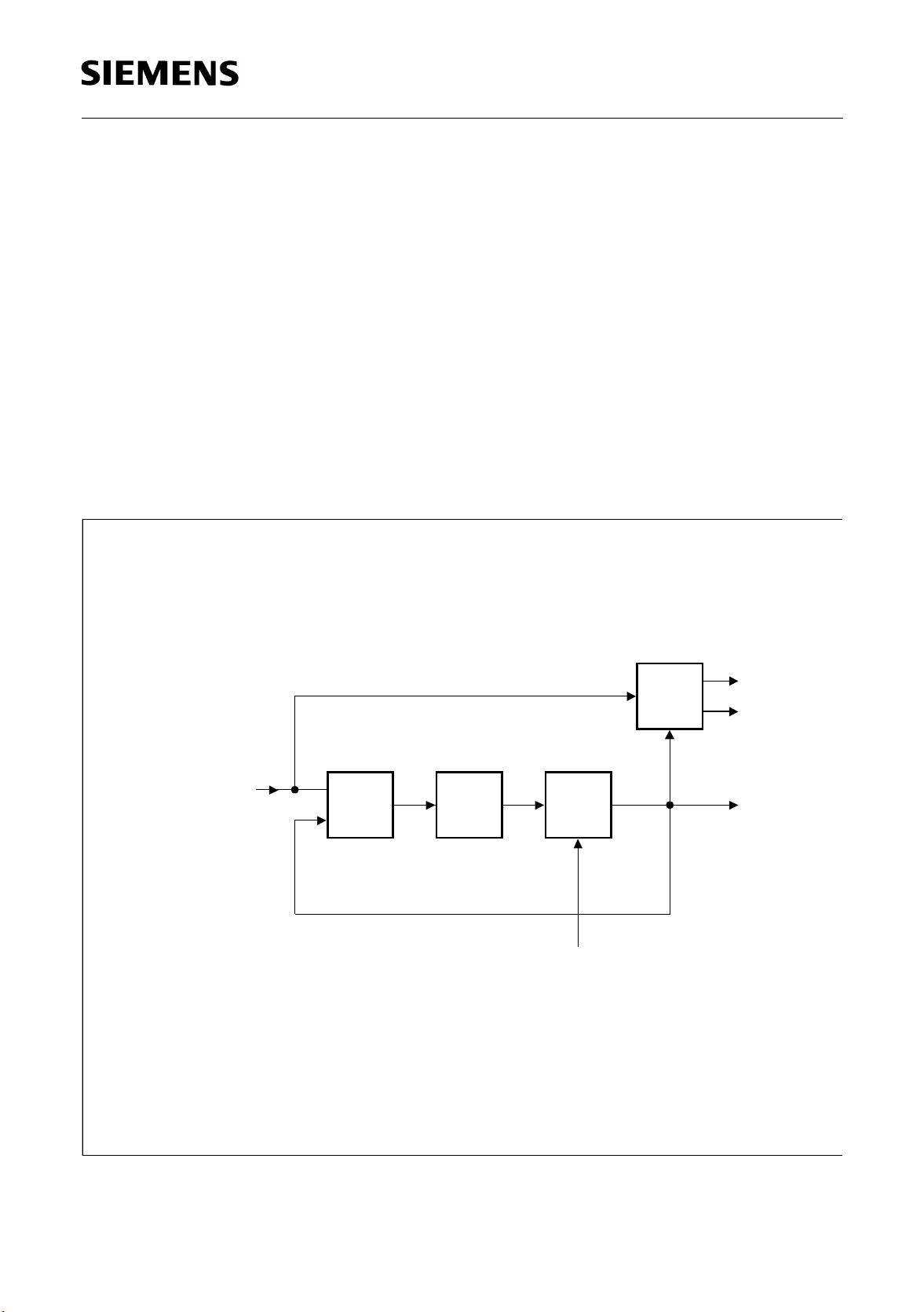
2 Functional Description
MODE
SYNC
JATT
XTAL1, 2, 3, 4LL
PEB 22320
Functional Description
RL1
Receive
Input
RL2
XL1
Transmit
Output
XL2
Receiver
Local Loop
Driver
Clock &
Data
Recovery
Loss of
Signal
Detection
D/A
RRCLK
P
N
LOS
ROM
LS0, 1, 2
Jitter Attenuator
&
Clock Generator
Timing &
Pulseshaper
XTIP
Transmit
XTIN
Test Data
XCLK (T1)
System
Clocks
RCLK
RDOP
RDON
Remote Loop
RL
XDIP
XDIN
XCLK
(CEPT)
ITB04876
Figure 2
Functional Block Diagram of the PRACT
Semiconductor Group 11
PEB 22320
Functional Description
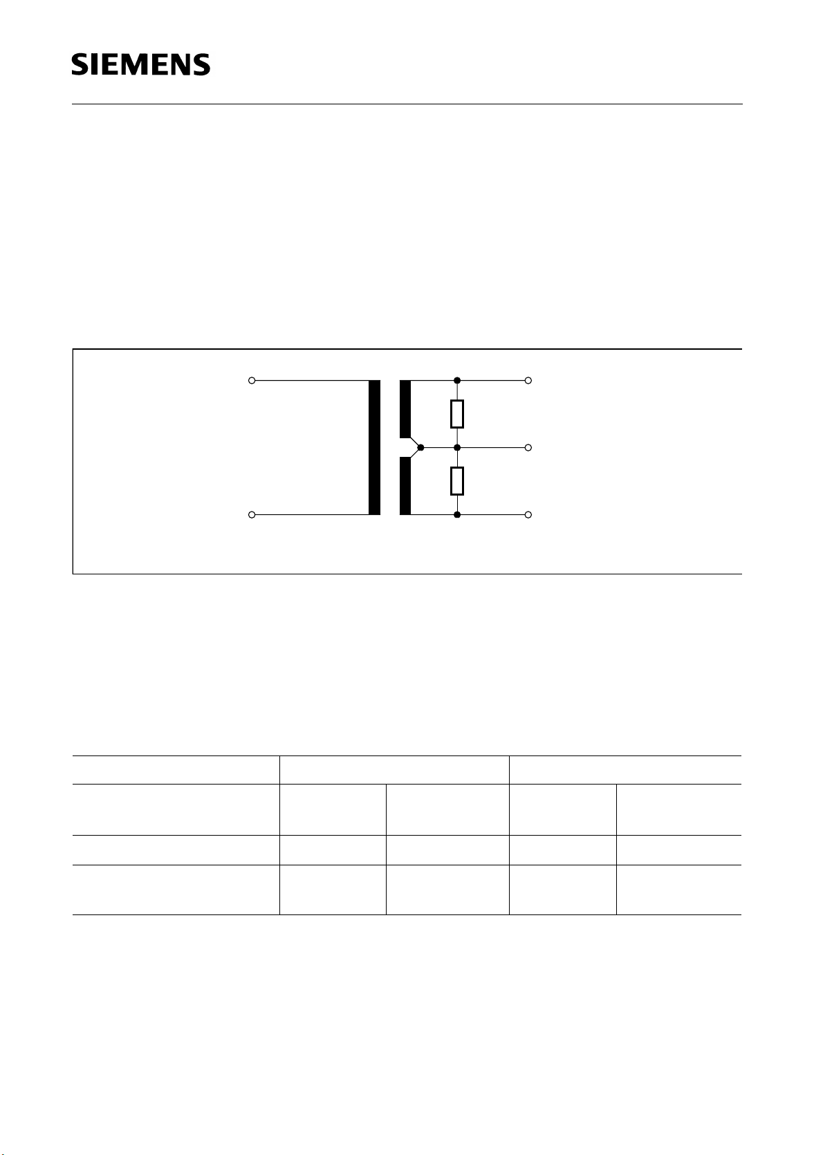
2.1 Receiver
2.1.1 Basic Functionality
The receiver recovers data from the ternary coded signal at the ternary interface and
outputs it as 2 unipolar signals at the dua l rail interface. One of the lines carries the
positive pulses, the other the negative pulses of the ternary signal.
The signal at the ternary interface is received at both ends of a center-tapped
transformer as shown in figure 3.
.
R
1
L
t
11
R
2
Line
t
2
R
t
12
2
V
2
DD
R
L
2
ITS00560
Figure 3
Receiver Configuration
The transformer is center-tapped at the PRACT si de. The recommended transmiss ion
factors for the different line characteristic impedances are listed in table 1.
Table 1
Recommended Receiver Configuration Values
Application T1 CEPT
Characteristic
100 140 (ICOT) 120 75
Impedances [Ω]
R
± (2.5%) [Ω]
2
t
:
t
=
t
: (t11 + t12)
2
1
2
28.7 39.2 60 60
69:52
69:(26 + 26)
69:52
69:(26 + 26)
Wired in this way the receiver has a return loss
a
> 12 dB for 0.025 f
r
a
> 18 dB for 0.05 f
r
a
> 14 dB for 1.0 f
with
r
f
being 2048 kHz. Thus it complies with CCITT G.703.
b
b
Semiconductor Group 12
≤ f ≤ 0.05 fb,
b
≤ f ≤ 1.0 fb and
b
≤ f ≤ 1.5 fb,
52:52
52:(26 + 26)
41:52
41:(26 + 26)
PEB 22320
Functional Description
The receiver is transparen t to the log ical 1’s p olarity and outputs pos itive logic al 1’s on
RDOP and negative logi cal 1’s on RDON. RDON and RDOP are activ e low and fully
bauded. The comparator threshold to detect logical 1’s and logica l 0’s is automatically
adjusted to be 45% of the peak signal level.
Provided the noise is below 10 µV/√Hz the bit error rate will be less than 10
2.1.2 Clock and Data Recovery
An analog PLL extracts the internal recovered route clock RRCLK from the data stream
received at the RL1 and RL2 lines. The PLL uses as a reference the system clock
CLK16M for CEPT and CLK12M for T1 applications. The clock and data re covery is
tolerant to long strings of consecutive zeros, because the data sampler will continuously
sample data based on its last input. A block diagram of the clock and data recovery
circuit is shown in figure 4.
–7
.
Input Data
derived from RL
1, 2
PD
Filter
VCO
CLK16M (CEPT)
CLK12M (T1)
Data
Sampling
P
Data
N
RRCLK
ITS04877
Figure 4
Clock and Data Recovery Circuit
Semiconductor Group 13
PEB 22320
Functional Description
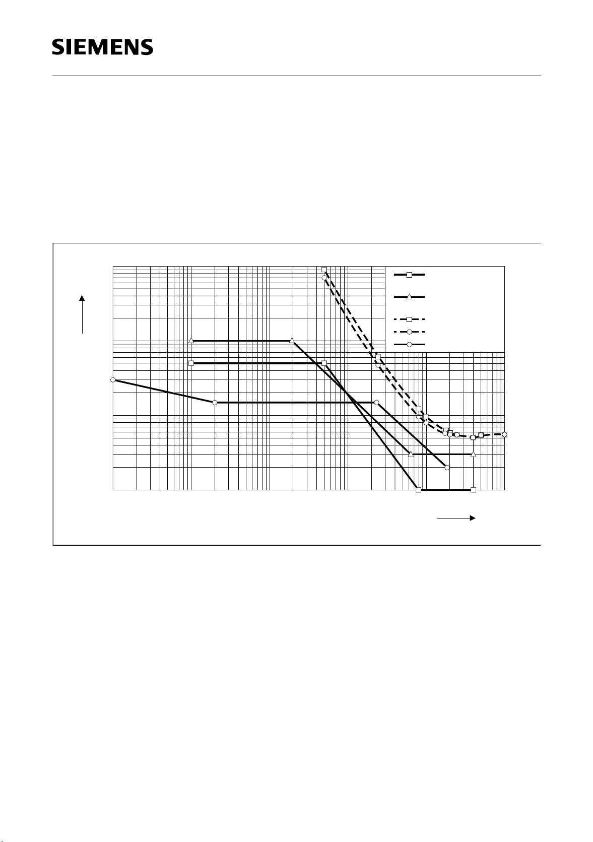
2.1.3 Input Jitter Tolerance
The PRACT receiver’s tolerance to input jitter complies to CCITT and Bellcore
requirements for CEPT and T1 application.
Figure 5 shows the curves of the different input jitter specifications stated above as well
as the PRACT performance for the various line codes used at the S1/S2 interfaces.
In figure 5 the curves show that the PRACT at low frequ encies has more than 20 dB/
decade fall off, and at high frequencies is in a steady state of 0.5 UI (horizontal).
100
UI
10
Jitter Input Tolerance
1
0.1
1 10 100 1000 10000 100000Hz
Jitter Frequency
ITD06576
TR-NWT 000499
Cat I
000499TR-NWT
IICat
PRACT CEPT
PRACT T1
CCITT G.823
Figure 5
Comparison of Input Jitter Specification and PRACT Performance
Semiconductor Group 14
 Loading...