


ICs for Communications
Octal Transceiver for U
OCTAT-P
PEB 2096 Version 1.3
Data Sheet 01.96
Interfaces
PN
T2096-V13-D2-7600

PEB 2096
Revision History: Current Version: 01.96
Previous Version: Technical Manual 11.93
Page
(in Version
11.93)
Page
(in new
Version)
Subjects (major changes since last revision)
17 New description of synchronization to the DCL frequency
18 22 New Version 1.3 number
26 New description of loop length
30 New description of the transmit delay on U
IOM-2 interface
48 New bit in the Configuration Register for U
37 50 Changed DC characteristics on LIna,b
39 53 Better jitter description
42 58 Changed SSYNC
60 New description of U
timing
frame relation to FSC
PN
interface in respect to
PN
Line Interfaces: EQUDIS
PN
Edition 01.96
This edition was realized using the software system FrameMaker
Published by Siemens AG,
Bereich Halble iter, Marketing-
Kommunikation, Balanstraße 73,
81541 München
©
Siemens AG 1996.
All Rights Re s e rv e d .
Attention please!
As far as patents or other rights of third parties are concerned, liability is only assumed for components, not for applications, processes and circuits implemented within components or assemblies.
The information describes the type of component and shall not be considered as assured characteristics.
Terms of delivery and rights to change design reserved.
For questions on technology, delivery and prices please contact the Semiconductor Group Offices in Germany or the S iemens Com-
panies and Representatives worldwide (see address list).
Due to technical requirements components may contain dangerous substances. For information on the types in question please con-
tact your nearest Siemens Office, Semiconductor Group.
Siemens AG is an approved CECC manufacturer.
Packing
Please use the recycling operators known to you. We can also help you – get in touch with your nearest sales office. By agreement
we will take packing material back, if it is sorted. You must bear the costs of transport.
For packing material that is returned to us unsorted or which we are not obliged to accept, we shall have to i nvoice you for any costs
incurred.
Components used in life-support devices or systems must be expressly authorized for such purpose!
Critical components
express written approval of the Semiconductor Group of Siemens AG.
1 A critical component is a component used in a life-support device or system whose fa ilure can reasonably b e expected to cause
the failure of that life-support device or system, or to affect its safety or effectiveness of that device or system.
2 Life support devices or systems are intended (a) to be implanted in the human body, or (b) to support and/or maintain and sustain
human life. If they fail, it is reasonable to assume that the health of the user may be endangered.
1
of the Semiconductor Group of Siemens AG, may only be used in life-support devices or systems2 with the
.

PEB 2096
Table of Contents Page
1Overview . . . . . . . . . . . . . . . . . . . . . . . . . . . . . . . . . . . . . . . . . . . . . . . . . . . . .5
1.1 Features . . . . . . . . . . . . . . . . . . . . . . . . . . . . . . . . . . . . . . . . . . . . . . . . . . . . . .8
1.2 Logic Symbol . . . . . . . . . . . . . . . . . . . . . . . . . . . . . . . . . . . . . . . . . . . . . . . . . .9
1.3 Pin Configuration . . . . . . . . . . . . . . . . . . . . . . . . . . . . . . . . . . . . . . . . . . . . . .10
1.4 Pin Definitions and Functions . . . . . . . . . . . . . . . . . . . . . . . . . . . . . . . . . . . . .11
1.5 Block Diagram . . . . . . . . . . . . . . . . . . . . . . . . . . . . . . . . . . . . . . . . . . . . . . . .13
2 Functional Description . . . . . . . . . . . . . . . . . . . . . . . . . . . . . . . . . . . . . . . .14
2.1 Device Architecture . . . . . . . . . . . . . . . . . . . . . . . . . . . . . . . . . . . . . . . . . . . .14
2.2 Interfaces . . . . . . . . . . . . . . . . . . . . . . . . . . . . . . . . . . . . . . . . . . . . . . . . . . . .14
2.2.1 General Principle of the U
2.2.2 IOM
®
-2 System Interface . . . . . . . . . . . . . . . . . . . . . . . . . . . . . . . . . . . . . . . .17
2.2.3 JTAG Boundary Scan Test Interface . . . . . . . . . . . . . . . . . . . . . . . . . . . . . . .19
2.2.3.1 Boundary Scan Test . . . . . . . . . . . . . . . . . . . . . . . . . . . . . . . . . . . . . . . . . . . .20
2.2.3.2 TAP Controller . . . . . . . . . . . . . . . . . . . . . . . . . . . . . . . . . . . . . . . . . . . . . . . .21
2.3 Individual Functions . . . . . . . . . . . . . . . . . . . . . . . . . . . . . . . . . . . . . . . . . . . .24
2.3.1 Transceiver, Analog Connections . . . . . . . . . . . . . . . . . . . . . . . . . . . . . . . . .24
2.3.2 Transmit PLL . . . . . . . . . . . . . . . . . . . . . . . . . . . . . . . . . . . . . . . . . . . . . . . . .26
2.3.3 Receive PLL . . . . . . . . . . . . . . . . . . . . . . . . . . . . . . . . . . . . . . . . . . . . . . . . . .26
2.3.4 Receive Signal Oversampling . . . . . . . . . . . . . . . . . . . . . . . . . . . . . . . . . . . .27
2.3.5 Activation / Deactivation . . . . . . . . . . . . . . . . . . . . . . . . . . . . . . . . . . . . . . . . .28
2.3.6 Diagnostic Functions . . . . . . . . . . . . . . . . . . . . . . . . . . . . . . . . . . . . . . . . . . .28
Interface . . . . . . . . . . . . . . . . . . . . . . . . . . . . . .14
PN
3 Operational Description . . . . . . . . . . . . . . . . . . . . . . . . . . . . . . . . . . . . . . .29
3.1 General . . . . . . . . . . . . . . . . . . . . . . . . . . . . . . . . . . . . . . . . . . . . . . . . . . . . .29
3.2 Clocking, Reset and Initialization . . . . . . . . . . . . . . . . . . . . . . . . . . . . . . . . . .29
3.3 Push – Pull Sensing on Pin DU . . . . . . . . . . . . . . . . . . . . . . . . . . . . . . . . . . .29
3.4 Transmit Delay on U
Interface in respect to IOM®-2 Interface . . . . . . . . . .30
PN
3.5 UPN Multiframe Synchronization . . . . . . . . . . . . . . . . . . . . . . . . . . . . . . . . . .31
3.5.1 Synchronization with a Short FSC . . . . . . . . . . . . . . . . . . . . . . . . . . . . . . . . .31
3.5.2 Synchronization using SSYNC (for DECT) . . . . . . . . . . . . . . . . . . . . . . . . . .31
3.6 D-Channel Handling . . . . . . . . . . . . . . . . . . . . . . . . . . . . . . . . . . . . . . . . . . . .32
®
3.7 IOM
-2 Interface Monitor Channel . . . . . . . . . . . . . . . . . . . . . . . . . . . . . . . . .35
3.8 Command / Indicate Channel . . . . . . . . . . . . . . . . . . . . . . . . . . . . . . . . . . . . .38
3.9 Activation and Deactivation, State Machine . . . . . . . . . . . . . . . . . . . . . . . . . .40
3.9.1 States Description . . . . . . . . . . . . . . . . . . . . . . . . . . . . . . . . . . . . . . . . . . . . .40
3.9.2 Info Structure on the U
Interface . . . . . . . . . . . . . . . . . . . . . . . . . . . . . . . .43
PN
3.9.3 Example of Activation and Deactivation . . . . . . . . . . . . . . . . . . . . . . . . . . . . .45
4 Registers Description . . . . . . . . . . . . . . . . . . . . . . . . . . . . . . . . . . . . . . . . .46
4.1 Identification Register – (Read) . . . . . . . . . . . . . . . . . . . . . . . . . . . . . . . . . . .46
4.2 General Configuration Register – (Write) . . . . . . . . . . . . . . . . . . . . . . . . . . . .47
4.3 Bit Error Register – (Read) . . . . . . . . . . . . . . . . . . . . . . . . . . . . . . . . . . . . . . .47
4.4 Configuration Regi ster for U
Line Interfaces – (Write) . . . . . . . . . . . . . . . .48
PN
Semiconductor Group 3 01.96

PEB 2096
Table of Contents Page
4.5 Test Registers – (Read/Write) . . . . . . . . . . . . . . . . . . . . . . . . . . . . . . . . . . . .48
5 Electrical Characteristics . . . . . . . . . . . . . . . . . . . . . . . . . . . . . . . . . . . . . .49
5.1 Absolute Maximum Ratings . . . . . . . . . . . . . . . . . . . . . . . . . . . . . . . . . . . . . .49
5.2 DC Characteristics . . . . . . . . . . . . . . . . . . . . . . . . . . . . . . . . . . . . . . . . . . . . .50
5.3 Capacitances . . . . . . . . . . . . . . . . . . . . . . . . . . . . . . . . . . . . . . . . . . . . . . . . .52
5.4 AC Characteristics . . . . . . . . . . . . . . . . . . . . . . . . . . . . . . . . . . . . . . . . . . . . .53
5.5 Clocks . . . . . . . . . . . . . . . . . . . . . . . . . . . . . . . . . . . . . . . . . . . . . . . . . . . . . .54
®
5.6 Timing of the IOM
5.7 Boundary Scan Timing . . . . . . . . . . . . . . . . . . . . . . . . . . . . . . . . . . . . . . . . . .58
5.8 U
Frame Relation to FSC in Transmit Direction . . . . . . . . . . . . . . . . . . . . .60
PN
5.9 Transceiver Characteristics . . . . . . . . . . . . . . . . . . . . . . . . . . . . . . . . . . . . . .61
6 Package Outlines . . . . . . . . . . . . . . . . . . . . . . . . . . . . . . . . . . . . . . . . . . . . .63
Interface . . . . . . . . . . . . . . . . . . . . . . . . . . . . . . . . . . . . .55
IOM®, IOM®-1, IOM®-2, SICOFI®, SICOFI®-2, SICOFI®-4, SICOFI®-4µC, SLICOFI®, ARCOFI
ARCOFI
SICAT
MUSAC
Purchase of Siemens I
the I
®
-SP, EPIC®-1, EPIC®-S, ELIC®, IPAT®-2, ITAC®, ISAC®-S, ISAC®-S TE, ISAC®-P, ISAC®-P TE, IDEC®,
®
, OCTAT®-P, QUAT®-S are registered trademarks of Siemens AG.
™
-A, FALC™54, IWE™, SARE™, UTPT™, ASM™, ASP™ are trademarks of Siemens AG.
2
2
C-system provided the system confor ms to the I2C specifications defined by Philips. Copyright Philips 1983.
C components conveys a license under the Philips’ I2C patent to use the components in
®
, ARCOFI®-BA,
Semiconductor Group 4 01.96

PEB 2096
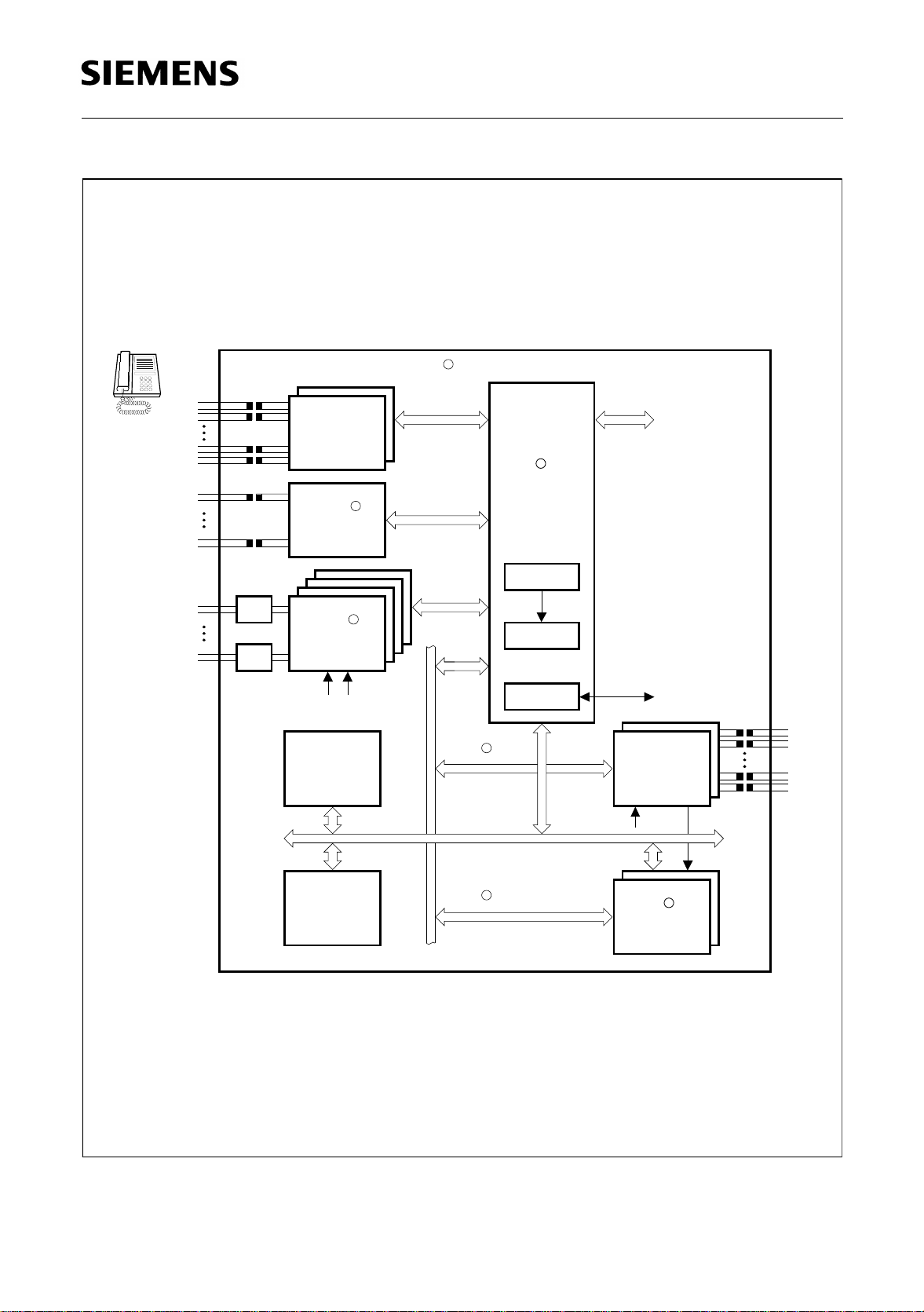
1Overview
A Line Card or a PBX consists of a li ne card co ntrol ler, mu ltip le layer-1 transceivers for
t/r (a/b), S/T, U
and U
P
power supply, transformers, etc. The new Siemens generation of highly integrated
ISDN circuits enables design Engineers to decrease bo ard size an d thus PBX size and
its production costs.
Figure 1 shows an example of a PBX for up to 16 ISDN and 16 analog subscribers with
4 trunk lines realized with a few highly integrated chips of the new Siemens family of PBX
and Line Cards ICs: ELIC, SICOFI-4, OCTAT-P, QUAT-S and IDEC.
ELIC, Enhanced Line Card Controller, PEB 20550, comprises the following functio nal
blocks on a single chip:
• Extended PCM Interface Controller (EPIC-1), which can switch up to 32 digital (ISDN)
or 64 voice (analog) subscribers,
• Two HDLC interface controllers (SACCO-A and SACCO-B),
• One D-channel arbiter to multiplex one HDLC controller (SACCO-A) to multiple
subscribers.
interfaces, signaling controllers, a microprocessor, memory,
2B1Q
The ELIC is a CMOS device offered in a P-MQFP-64 package.
OCTAT-P
The Octal Transceiver for U
interfaces, PEB 2096, implements the two-wire U
PN
PN
interface used to link voice/data digital terminals to PBX subscriber lines. The OCTAT-P
is an optimized d evice for LT applications and can handle up to eight U
simultaneously. It handles the U
interfaces in accordance with the UP0 interface
PN
interfaces
PN
specification except for the reduced loop length.
The OCTAT-P is a CMOS device offered in a P-MQFP-44 package.
QUAT-S
The Quadruple Transceiver for S/T Interfaces, PEB 2084, implements 4 four-wire S/T
interfaces to link voice/data digital termi nals to PBX subscriber lines or PBX trunk lines
to the public ISDN. It can handle up to four S/T interfaces simultaneously in accordance
with CCITT I.430, ETSI 300.012, and ANSI T1.605 standards.
The QUAT-S is a CMOS device offered in a P-MQFP-44 package.
IDEC
The ISDN D-Channel Exchange Controller, PEB 2075, is an HDLC controller which
handles four HDLC communication channels. Each channel is fully independent and
programmable by its own register set.
The IDEC is a CMOS device offered in a P-LCC-44 and P-DIP-28 package.
Semiconductor Group 5 01.96
8 x S
8 x U
PN
TE 0
TE 7
TE 0
TE 7
PEB 2096
R
IOM -2
2048 kbit/s
S
0
U
PN
QUAT-S
PEB 2084
OCTAT -P
R
PEB 2096
CFI
00
ELIC
PCM
PCM
R
PEB 20550
1
16 x t/r
TE 1
TE 16
SLIC
r/t
SLIC
R
SICOFI -4
PEB 2465
T
SS
Memory
µP
R
IOM -2
R
IOM -2
D Arbiter
2
SACCO-A
3
SACCO-B
µP Interface
4 x D Cannel
Signaling
QUAT-S
2084PEB
R
IDEC
PEB 2075
8 x T
0
CO
7
ITB05392
Figure 1
Application Example for a PBX
Semiconductor Group 6 01.96

PEB 2096
SICOFI®-4
The programmable Signaling and CODEC Filter with 4 channels, PEB 2465, implements
4 t/r (a/b) interfaces to link analog voice terminals to PBX subscriber lines or analog PBX
trunk lines to public switches. An integrated Digital Signal Processor handles all the
algorithms necessary, e.g. transhybrid-loss adaption, gain, frequency response,
impedance matching. The IOM-2 Interface handles digital voice transmission, SICOFI-4
feature control and transpa rent access to the SICO FI-4 command and indic ation pins.
To program the filters, precalculated sets of coefficients are downloaded from the
system to the on-chip coefficient R AM. Thus it is possible to use the sam e line card in
different countries.
The SICOFI-4 is a CMOS device offered in a P-MQFP-64 package.
®
ISDN-Oriented Modular Interface (IOM
The IOM-2 interface is a four -wire interface which has been defined by the “Group of
Four”: ALCATEL, Siemens, Plessey and ITALTEL systems houses. It became a
standard interface for interchip communication in ISDN applications.
-2)
All ICs described above are compatible to the IOM-2 interface and operate from a single
5 V power supply (incl. SICOFI-4).
Semiconductor Group 7 01.96
Octal Transceiver for U
Interfaces
PN
PEB 2096
OCTAT-P
Version 1.3 CMOS
1.1 Features
• Eight full duplex 2B+D U
each equipped with the following functions:
– Conversion from/to binary to/from pseudo-ternary
code
– Receive timing recovery
– Activation/deactivation procedures, triggered by
primitives received over the IOM interface or by
INFO received from the line (e.g. detection of
INFO 1)
– Execution of test loops
– Analog line transceiver for up to 16 dB line attenuation
–U
interface functions compatible to PEB 2095, IBC,
PN
and PEB 20950, ISAC-P (except for looplength)
–U
interface fully compatible to PSB 2196, ISAC-P TE,
PN
and PSB 2197, SmartLink-P.
• IOM-2 interface
• Support for JTAG boundary scan test
•1µ CMOS technology with low power consumption
• P-MQFP-44 package
interface transceivers,
PN
P-MQFP-44
Note: UPN refers to a version of the standard interface UP0 (according to ZVEI standard)
with a reduced loop length (up to 1.3 km).
Type Ordering Code Package
PEB 2096 Q67100-H6422 P-MQFP-44
Semiconductor Group 8 01.96
1.2 Logic Symbol
PEB 2096
Figure 2
Semiconductor Group 9 01.96
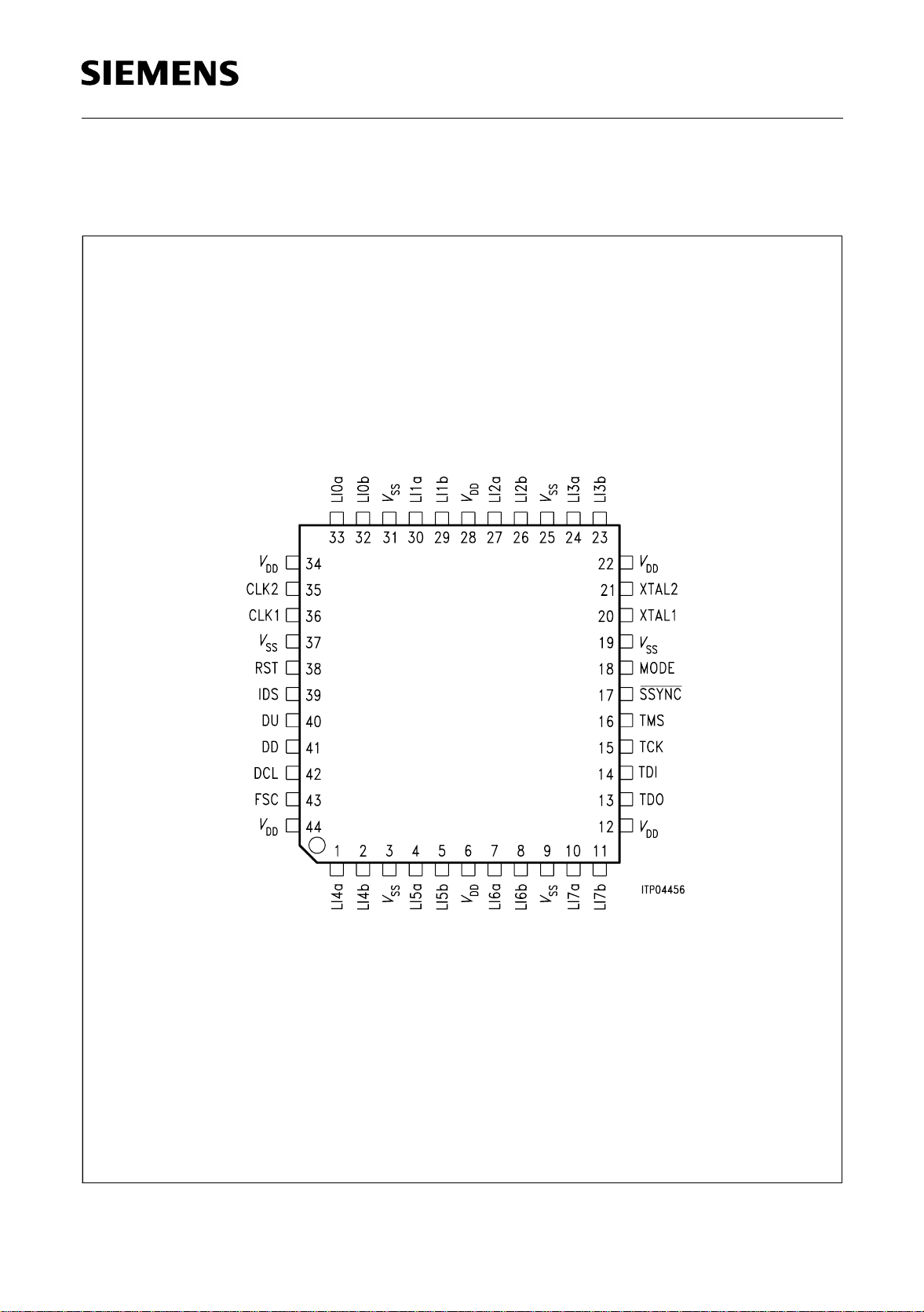
1.3 Pin Configuration
(top view)
PEB 2096
P-MQFP-44
Figure 3
Semiconductor Group 10 01.96

1.4 Pin Definitions and Functions
PEB 2096
Pin No. Symbol Input (I)
Output (O)
6, 12, 22, 28,
V
DD
I
34, 44
3, 9, 19,
V
SS
I
25, 31, 37
33, 32
30, 29
27, 26
24, 23
1, 2
4, 5
7, 8
10, 11
43
42
41
40
39
LI0a,b
LI1a,b
LI2a,b
LI3a,b
LI4a,b
LI5a,b
LI6a,b
LI7a,b
FSC
DCL
DD
DU
IDS
I/O
I/O
I/O
I/O
I/O
I/O
I/O
I/O
I
I
I
O
I
Function
+ 5 V power supply
Reference ground
Line Interfaces a,b
U
PN
No. 0: differential input / output
No. 1: differential input / output
No. 2: differential input / output
No. 3: differential input / output
No. 4: differential input / output
No. 5: differential input / output
No. 6: differential input / output
No. 7: differential input / output
®
-2 Interface
IOM
Frame Synchronization Cl ock : 8 kHz
Data Clock
Data Downstream (data input)
Data Upstream (data output)
Interface Data rate Select (static pin-strapped):
0: double DCL (normal IOM interface)
1: single DCL
JTAG Boundary Scan Interface
16
15
14
13
20
21
TMS
TCK
TDI
TDO
I
I
I
O
XTAL1
XTAL2IO
Test Mode Select, internal pull-up resistor
Test Clock
Test Data Input, internal pull-up resistor
Test Data Output
Oscillator or 15.36 MHz clock input
Oscillator output
36 CLK1 O Clock output 15.36 MHz
(i.e. to drive other OCTAT-P)
35 CLK2 O Clock output 7.68 MHz
(i.e. to drive ISAC-S or QUAT-S)
38 RST I Reset, active high
Semiconductor Group 11 01.96

1.4 Pin Definitions and Functions (cont’d)
PEB 2096
Pin No. Symbol Input (I)
Function
Output (O)
18 SSYNC I Superframe synchronization
17 MODE I This pin selects the initial values of the General
Configuration Register and in the Configuration
Register for U
Line Interfaces as described in
PN
chapters 4.2 and 4.4. It also enables Push-Pull
Sensing on pin DU as described in chapter 3.3.
Semiconductor Group 12 01.96
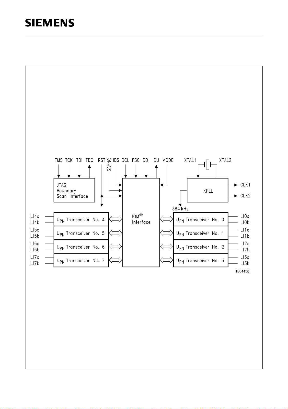
1.5 Block Diagram
PEB 2096
Figure 4
Semiconductor Group 13 01.96

PEB 2096
2 Functional Description
The PEB 2096, OCTAT-P, performs the layer-1 functions of the ISDN basic access for
eight U
2.1 Device Architecture
The OCTAT-P contains the following functional blocks: Refer to figure 4
interfaces at the LT side of the PBX.
PN
• Eight line transceivers for the U
interfaces
PN
• One IOM-2 interface
• Frame structure converter between the IOM-2 interface and the U
interfaces
PN
• JTAG Boundary scan interface
• Clocking, reset and initialization block
2.2 Interfaces
2.2.1 General Principle of the U
Interface
PN
A frame transmitted by the e xchange (LT) is received by the terminal eq uipment (TE)
t
after a given propagation delay (
minimum guard time (
t
=5.2 µs) while the line clears. It then transmits a frame to the
g
). Refer to figure 5. The terminal equipment waits a
d
exchange. The exchange begins a transmission every 250 µs (known as the burst
repetition period). However, the time between the reception of a frame from the TE and
the beginning of transmission of the next frame by the LT must be greater than the
minimum guard time. Communication b etween an LT and a PT (Private Termination)
follows exactly the same procedure.
Note that the guard time in TE is always defined with respect to the M-bit.
Semiconductor Group 14 01.96
LT
TE/PT
PEB 2096
t
r
d
LF B1 B2
1
8
1)
M Channel Superframe
CV = Code Violation: for Superframe synchronization
t = Transparent Channel (2
S = Service Channel (1
2)
DC balancing bit, only sent after a code violation in the
M-bit position and in special configurations.
Timings: =burst repetition period
tt
g
8
t
r
=line delay
t
d
=guard time
t
g
D
4
99
s
µ
LF-Framing Bit
kbit/s)
kbit/s)
s
µ
= 20.8
= 5.2
µ
s
t
d
B2B1
8
CVTSTCVTSTCV
µ
s
= 250
maximum
minimum
8
)
1
M
DC
#Bits
1
ITD00823
2)
Figure 5
U
Interface Frame Structure (= UPN)
P0
Within a burst, the data rate is 384 kbit/s. The 38-bit frame structure is as shown in
figure 5. The framing bit (LF) is always logical ‘1’. The frame also contains the user
channels (2B + D).
It can readily be seen that in the 250 µs burst repetition p erio d, 4 D bi ts, 1 6 B1 b its and
16 B2 bits are transferred in each direct ion. This results in an effective full dup lex data
rate of 16 kbit/s for the D channel and 64 kbit/s for each B channel.
The final bit of the frame is called the M bit. It´s data rate is 4 kbit/s. Four successive
M bits, from four successive U frames, constitute a superframe. Three signals are
carried in this superfra me. Every fourth M bit is a code v iolation (CV) and is used for
superframe synchronization. This can be regarded as the first bit of the superframe.
Semiconductor Group 15 01.96
PEB 2096
From this reference (CV = bit 1), bit 3 of the superframe is the service channel bit S. This
S-channel bit is transmitted once in each direction in every fourth burst repetition period.
Hence the duplex S channel has a data rate of 1 kbit/s. It conveys test loop control
information from the LT to the TE/PT and reports of transmission errors from the TE/PT
to the LT. Bit 2 and bit 4 of the superframe are the T bits. This 2 kbit/s channel is
accessible via the C/I channel and may be used to carry the “available”/“blocked”
information sent by the D-channel arbiter of the PEB 20550, ELIC.
It is allowed to add a DC balancing bit to the burst, in order to decrease DC offset voltage
on the line after transmission of a CV in the M-bit position. The OCTAT-P transmits this
DC balancing bit when transmitting INFO 4 and when line characteristics indicate
potential decrease in performance.
The OCTAT-P scrambles B-channel data on the U
interface in order to ensure that the
PN
downstream receiver (e.g. ISAC-P TE) gets enough pulses for a reliable clock extraction
(flat continuous power density spectrum is provided) and no periodic patterns appear on
the line.
The scrambling is in accordance with CCITT V.27.
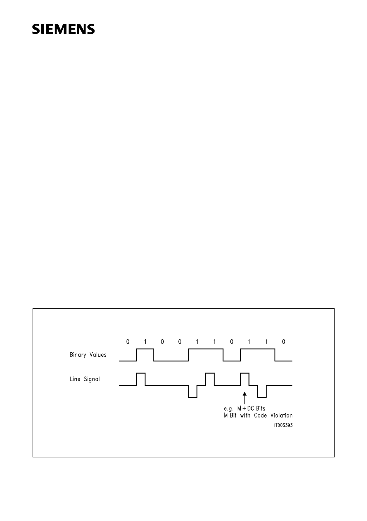
The coding technique used on the U in terface is a half-bauded AMI co de (with a 50 %
pulse width). A logical ‘0’ corresponds to a neutral level, logical ‘1’ are coded as alternate
positive and negative pulses. Code vi olation (CV) is caused b y two successive p ulses
with the same polarity.
See figure 6. The AMI coding includes always the da ta bits go ing on the UPN interface
in one direction. Thus there is a separate AMI coding unit for data downstream and one
for data upstream.
Figure 6
AMI Coding on the U
Semiconductor Group 16 01.96
Interface
PN
PEB 2096
2.2.2 IOM®-2 System Interface
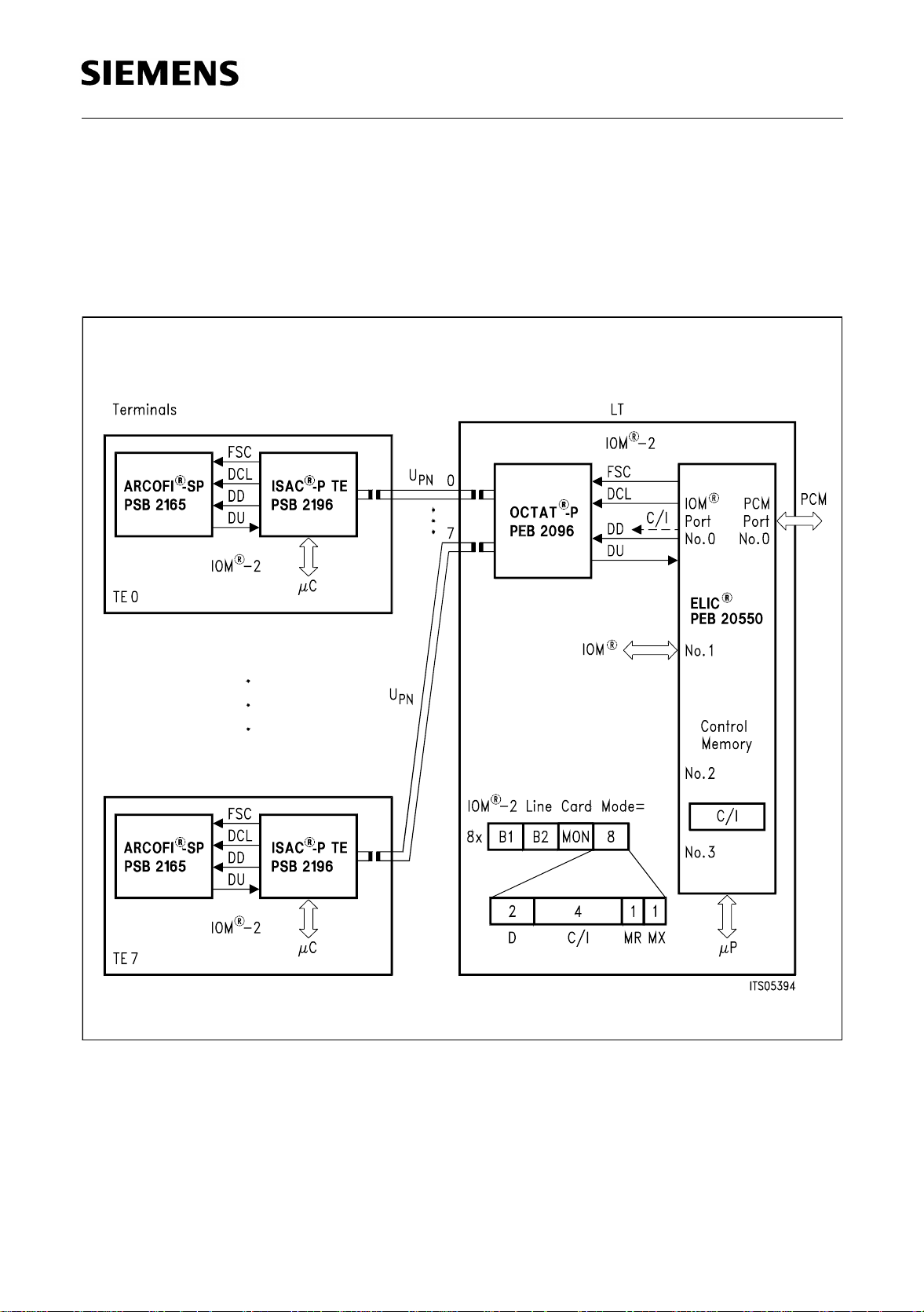
The PEB 2096, OCTAT-P, is equipped with a digital ISDN Oriented Modular (IOM-2)
interface, for communication with upper layer functions, such as IDEC (PEB 2075), EPIC
(PEB 2055) and ELIC (PEB 20550). EPIC and ELIC represent the first switchin g stage
towards the exchange system. Refer to figure 7.
Figure 7
®
System Integration, IOM
Interface
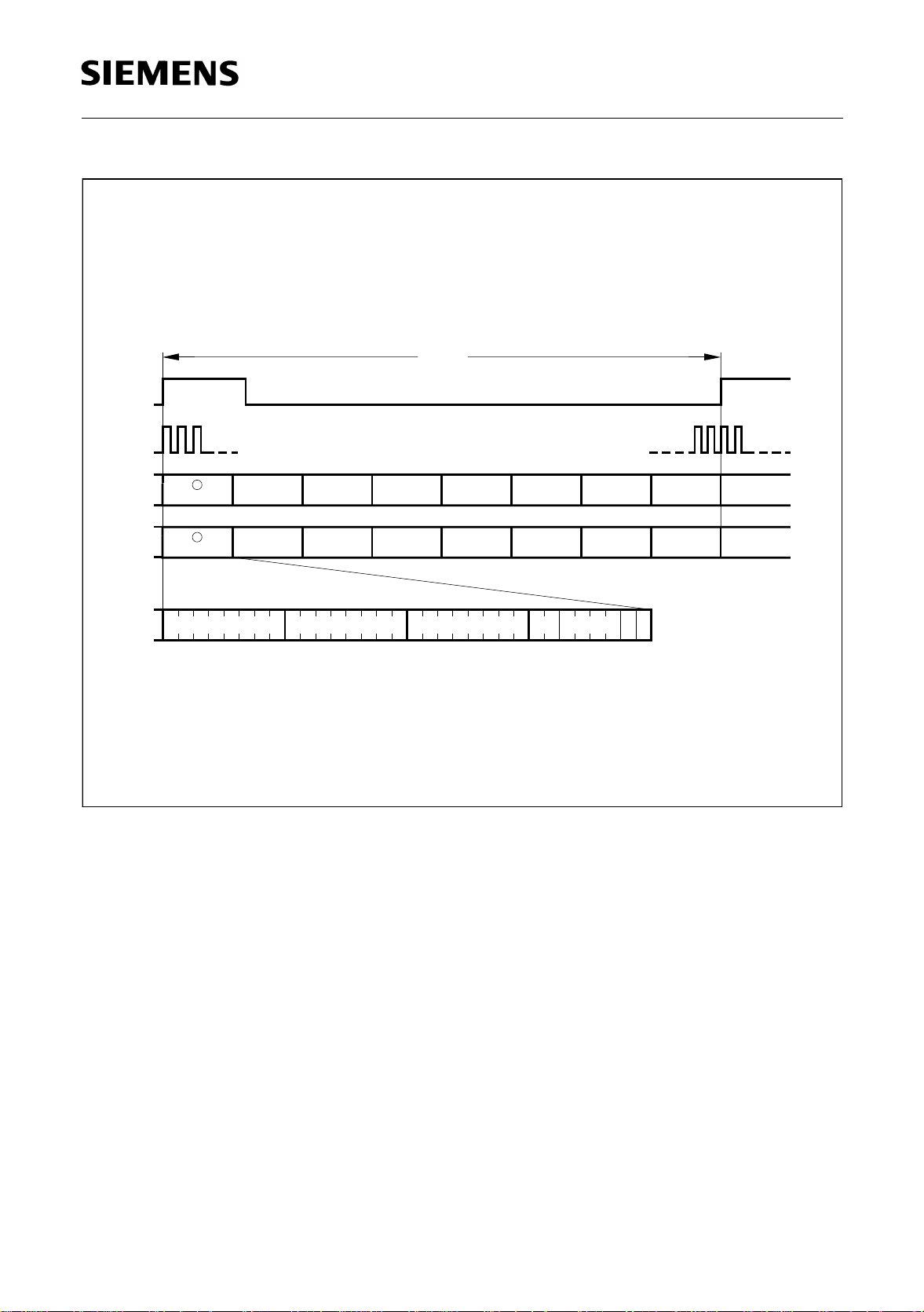
The IOM interface is a four-wire serial interface with a data clock (DCL), an 8 kHz frame
synchronization clock (FSC), and one data line per direction: data downstream (DD) and
data upstream (DU). One IOM-2 fra me consists of up to 8 IOM channels (s ubframes)
(figure 8).
Semiconductor Group 17 01.96
FSC
DCL
DU
s
µ
125
R
IOM
CH0 CH1 CH2 CH3 CH4 CH5 CH6 CH7
PEB 2096
CH0
DD
IOM
B1 B2
MONITOR
CH7CH6CH5CH4CH3CH2CH1CH0
C/I
MM
RX
D
CH0
ITD04319
R
Figure 8
Multiplexed Frame Structure of the IOM
®
-2 Interface in LT-Mode with 2.048 Mbit/s
Data Rate
Each IOM channel consists of a total of 32 bits, or four octets: B1 + B2 + D (18 bits) plus
14 overhead bits for monitor and control information (activation/deactivation of OSI
layer-1 and maintenance functions).
The ISDN user data rate is 144 kbit/s (B1 + B2 + D).
The data is transmitted transparently synchrono us and in phase in both directio ns over
the IOM interface using time division multiplexing within the 125 µs IOM-2 interface
frame.
Nominal bit rate of data (DD and DU): 256 kbit/s … 4096 kbit/s
Nominal frequency of DCL: 512 kHz … 8192 kHz
Nominal frequency of FSC: 8 kHz
Note: The bit rate must be a multiple of 256 kbit/s.
Semiconductor Group 18 01.96

PEB 2096
In order to allow the use of the eight channels also with a maximum clock rate of
2,048 kHz provided by the system , the OCTAT-P can also run the IOM interface with
only half the nominal DCL clock rate, i.e. 2,048 kHz for 2,048 kbit/s (Input pin IDS = 1).
The OCTAT-P requires three IOM frames to synchronize to the DCL frequency. A
corrupted IOM frame cau sed by different amount of DC L pul ses w ith in two consecutive
IOM frames (e.g. caused by spikes on DCL or FSC) resets internally all registers and the
activation and deactivation state machine, figure 21.
The allocation between U
line interfaces and the IOM-2 interface channels is
PN
according to their numbe rs, i.e. L I0a,b is alloca ted to IOM c hannel 0, LI1 to channel 1,
and so on.
For details refer to figures 14 and 15 and to the chapter 5.8 and the IOM Interface
Specification, Rev. 2.
Monitor Channel
The monitor channel is used to convey messages (e.g. when a bit error occurs on U
PN
or for access to internal registers: Identification Register, General Configuration
Register, Bit Error Register, Configuration Register for U
and Test Registers.
PN
The PEB 2096, OCTAT-P, has implemented the monitor channel protocol accord ing to
the IOM Interface Specification , Rev. 2, in the first of the eight IOM ch annels alloca ted
to the eight UPNinterfaces. Refer also to the chapter 3.7.
C/I-Channel
The C/I-channel is used for communica tion between the PEB 2096, OCTAT-P, and a
processor via a layer-2 device, to con trol and monitor la yer-1 functions. The OCTAT-P
has 8 IOM-2 channels and thus 8 C/I-channels; one for each transceiver.
)
The codes originating from layer-2 devices are called “commands”, those from the
PEB 2096, OCTAT-P, are called “indications”. For a list of the C/I (command/indication)
codes and their use, refer to the
chapters 3.8.
2.2.3 JTAG Boundary Scan Test Interface
The OCTAT-P provides fully IEEE Standard 1 149.1 co mpatibl e bound ary scan support
to allow cost effective board testing. It consists of:
• Complete boundary scan test
• Test access port controller (TAP)
• Four dedicated pins (TCK, TMS, TDI, TDO)
• One 32-bit IDCODE register
• Specific functions for LIna,b
Semiconductor Group 19 01.96
 Loading...