


ICs for Communications
Quadruple Transceiver for S/T Interface
QUAT-S
PEB 2084 Version 1.2
Data Sheet 07.95
T2084-V12-D1-7600

Ausgabe 07.95
Herausgegeben von Siemens AG,
Bereich Halbleiter, Marketing-
Kommunikation, Balanstraße 73,
81541 München
© Siemens AG 1995.
Alle Rechte vorbehalten.
Wichtige Hinweise!
Gewähr für die Freiheit von Rechten Dritter
leisten wir nur für Bauelemente selbst, nicht
für Anwendungen, Verfahren und für die in
Bauelementen oder Baugruppen realisier ten
Schaltungen.
Mit den Angaben werden die Bauelemente
spezifiziert, nicht Eigenschaften zugesich ert .
Liefermöglichkeiten und technische Änderungen vorbehalten.
Fragen über Technik, Preise und Liefermöglichkeiten richten Sie bitte an den Ihnen
nächstgelegenen Vertrieb Halbleiter in
Deutschland oder an unsere Landesgesellschaften im Ausland.
Bauelemente können aufgrund technischer
Erfordernisse Gefahrstoffe enthalten. Auskünfte darüber bitten wir unter Angabe des
betreffenden Typs ebenfalls über den Vertrieb
Halbleiter einzuholen.
Die Siemens AG ist ein Hersteller von CECCqualifizierten Produkten.
Verpackung
Bitte benutzen Sie die Ihnen bekannten Verwerter. Wir helfen Ihnen auch weiter – wenden Sie sich an Ihren für Sie zuständigen Vertrieb Halbleiter. Nach Rücksprache nehmen
wir Verpackungsmaterial sortiert zurück. Die
Transportkosten müssen Sie tragen.
Für Verpackungsmaterial, das unsort i ert an
uns zurückgeliefert wird oder für das wir keine
Rücknahmepflicht haben, müssen wir Ihnen
die anfallenden Kosten in Rechnung stellen.
Bausteine in lebenserhaltenden Geräten
oder Systemen müssen ausdrücklich dafür zugelassen sein!
Kritische Bauelemente
ter der Siemens AG dürfen nur mit ausdrücklicher schriftlicher Genehmigung des Bereichs
Halbleiter der Siemens AG in lebenserhaltenden Geräten oder Systemen
den.
1 Ein kritisches Bauelement ist ein in einem
lebenserhaltenden Gerät oder System eingesetztes Bauelement, bei dessen Ausfall
berechtigter Grund zur Annahme besteht,
daß das lebenserhaltende Gerät oder System ausfällt bzw. dessen Sicherheit oder
Wirksamkeit beeinträchtigt wird.
2 Lebenserhaltende Geräte und Systeme
sind (a) zur chirurgischen Einpflanzung in
den menschlichen Körper gedacht, oder
(b) unterstützen bzw. erhalten das
menschliche Leben. Sollten sie ausfallen,
besteht berechtigter Grund zur Annahme,
daß die Gesundheit des Anwenders gefährdet werden kann.
1
des Bereichs Halblei-
2
eingesetzt wer-

PEB 2084
Revision History: Current Version: Data Sheet 07.95
Previous Releases: Preliminary Technical Manual 2.94
Page
(in previous
Version)
11 10 Figure 1, IDO = Output and Input
9 12 Pin 40, IDO, resistor definition
20 22 Boundary scan, sequence of test pins (new)
29 33 Push-pull sensing
43 44 State diagram (DI → F3)
55 60 Maximum voltage on any pin
56 63 Power supply current
Page
(in current
Version)
Subjects (major changes since last revision)

PEB 2084
Table of Contents Page
1Overview . . . . . . . . . . . . . . . . . . . . . . . . . . . . . . . . . . . . . . . . . . . . . . . . . . . . .6
1.1 Features . . . . . . . . . . . . . . . . . . . . . . . . . . . . . . . . . . . . . . . . . . . . . . . . . . . . . .8
1.2 Logic Symbol . . . . . . . . . . . . . . . . . . . . . . . . . . . . . . . . . . . . . . . . . . . . . . . . . .9
1.3 Pin Configuration . . . . . . . . . . . . . . . . . . . . . . . . . . . . . . . . . . . . . . . . . . . . .10
1.4 Pin Description . . . . . . . . . . . . . . . . . . . . . . . . . . . . . . . . . . . . . . . . . . . . . . . .11
2 Functional Description . . . . . . . . . . . . . . . . . . . . . . . . . . . . . . . . . . . . . . . .13
2.1 Device Architecture . . . . . . . . . . . . . . . . . . . . . . . . . . . . . . . . . . . . . . . . . . . .13
2.2 Interfaces . . . . . . . . . . . . . . . . . . . . . . . . . . . . . . . . . . . . . . . . . . . . . . . . . . . .14
2.2.1 S/T Interface . . . . . . . . . . . . . . . . . . . . . . . . . . . . . . . . . . . . . . . . . . . . . . . . . .14
®
2.2.2 IOM
2.2.3 JTAG Boundary Scan Test Interface . . . . . . . . . . . . . . . . . . . . . . . . . . . . . . .21
2.3 Individual Functions . . . . . . . . . . . . . . . . . . . . . . . . . . . . . . . . . . . . . . . . . . . .24
2.3.1 Transceiver, Analog Connections . . . . . . . . . . . . . . . . . . . . . . . . . . . . . . . . .24
2.3.2 Timing Recovery . . . . . . . . . . . . . . . . . . . . . . . . . . . . . . . . . . . . . . . . . . . . . .26
2.3.3 Receive Signal Oversampling . . . . . . . . . . . . . . . . . . . . . . . . . . . . . . . . . . . .27
2.3.4 Activation / Deactivation . . . . . . . . . . . . . . . . . . . . . . . . . . . . . . . . . . . . . . . . .29
2.3.5 S/T Interface Frame Structures Synchronization . . . . . . . . . . . . . . . . . . . . . .29
2.3.5.1 Multi-Frame Generation with a short FSC . . . . . . . . . . . . . . . . . . . . . . . . . . .30
2.3.5.2 Super-Frame (M-bit) Generation using SSYNC (for DECT) . . . . . . . . . . . . .31
-2 System Interface . . . . . . . . . . . . . . . . . . . . . . . . . . . . . . . . . . . . . . . .17
3 Operational Description . . . . . . . . . . . . . . . . . . . . . . . . . . . . . . . . . . . . . . .32
3.1 Reset . . . . . . . . . . . . . . . . . . . . . . . . . . . . . . . . . . . . . . . . . . . . . . . . . . . . . . .32
3.2 Push – Pull Sensing on Pin IDO . . . . . . . . . . . . . . . . . . . . . . . . . . . . . . . . . .32
®
3.3 IOM
-2 Interface . . . . . . . . . . . . . . . . . . . . . . . . . . . . . . . . . . . . . . . . . . . . . . .32
3.3.1 ISDN Channels Allocation . . . . . . . . . . . . . . . . . . . . . . . . . . . . . . . . . . . . . . .32
3.3.2 Monitor Channel . . . . . . . . . . . . . . . . . . . . . . . . . . . . . . . . . . . . . . . . . . . . . . .33
3.3.3 D-Channel Handling . . . . . . . . . . . . . . . . . . . . . . . . . . . . . . . . . . . . . . . . . . . .36
3.3.4 Command/Indicate Channel . . . . . . . . . . . . . . . . . . . . . . . . . . . . . . . . . . . . . .40
3.4 Activation and Deactivation . . . . . . . . . . . . . . . . . . . . . . . . . . . . . . . . . . . . . .40
3.4.1 LT-S Mode . . . . . . . . . . . . . . . . . . . . . . . . . . . . . . . . . . . . . . . . . . . . . . . . . . .41
3.4.2 LT-T Mode . . . . . . . . . . . . . . . . . . . . . . . . . . . . . . . . . . . . . . . . . . . . . . . . . . .45
3.4.3 Example of Activation/Deactivation . . . . . . . . . . . . . . . . . . . . . . . . . . . . . . . .50
3.5 Diagnostic Functions, Test Loop-backs . . . . . . . . . . . . . . . . . . . . . . . . . . . . .51
3.6 S and Q Channel Access . . . . . . . . . . . . . . . . . . . . . . . . . . . . . . . . . . . . . . . .52
3.7 Default-Use of Pin CEB/SSYNC
. . . . . . . . . . . . . . . . . . . . . . . . . . . . . . . . . .53
4 Registers Description . . . . . . . . . . . . . . . . . . . . . . . . . . . . . . . . . . . . . . . . .54
4.1 Identification Register . . . . . . . . . . . . . . . . . . . . . . . . . . . . . . . . . . . . . . . . . . .54
4.2 Configuration Register . . . . . . . . . . . . . . . . . . . . . . . . . . . . . . . . . . . . . . . . . .55
4.3 Loopback Register . . . . . . . . . . . . . . . . . . . . . . . . . . . . . . . . . . . . . . . . . . . . .56
4.4 Auxiliary Register . . . . . . . . . . . . . . . . . . . . . . . . . . . . . . . . . . . . . . . . . . . . . .57
4.5 Other Registers . . . . . . . . . . . . . . . . . . . . . . . . . . . . . . . . . . . . . . . . . . . . . . .58
Semiconductor Group 4

PEB 2084
Table of Contents Page
5 Electrical Characteristics . . . . . . . . . . . . . . . . . . . . . . . . . . . . . . . . . . . . . .59
5.1 Absolute Maximum Ratings . . . . . . . . . . . . . . . . . . . . . . . . . . . . . . . . . . . . . .59
5.2 DC Characteristics . . . . . . . . . . . . . . . . . . . . . . . . . . . . . . . . . . . . . . . . . . . . .61
5.3 Capacitances . . . . . . . . . . . . . . . . . . . . . . . . . . . . . . . . . . . . . . . . . . . . . . . . .62
5.4 Recommended Oscillator Circuits . . . . . . . . . . . . . . . . . . . . . . . . . . . . . . . . .63
5.5 AC Characteristics . . . . . . . . . . . . . . . . . . . . . . . . . . . . . . . . . . . . . . . . . . . . .63
5.6 Clocks . . . . . . . . . . . . . . . . . . . . . . . . . . . . . . . . . . . . . . . . . . . . . . . . . . . . . .64
®
5.7 IOM
5.8 Timing of Boundary Scan Test Interface . . . . . . . . . . . . . . . . . . . . . . . . . . . .68
5.9 Transceiver Characteristics . . . . . . . . . . . . . . . . . . . . . . . . . . . . . . . . . . . . . .69
6 Package Outlines . . . . . . . . . . . . . . . . . . . . . . . . . . . . . . . . . . . . . . . . . . . . .71
7 Appendix . . . . . . . . . . . . . . . . . . . . . . . . . . . . . . . . . . . . . . . . . . . . . . . . . . . .72
-2 Interface Timing . . . . . . . . . . . . . . . . . . . . . . . . . . . . . . . . . . . . . . . . .65
IOM®, IOM®-1, IOM®-2, SICOFI®, SICOFI®-2, SICOFI®-4, SICOFI®-4µC, SLICOFI®, ARCOFI
ARCOFI
SICAT
MUSAC
Purchase of Siemens I
the I
®
-SP, EPIC®-1, EPIC®-S, ELIC®, IPAT®-2, ITAC®, ISAC®-S, ISAC®-S TE, ISAC®-P, ISAC®-P TE, IDEC®,
®
, OCTAT®-P, QUAT®-S are registered trademarks of Siemens AG.
™
-A, FALC™54, IWE™, SARE™, UTPT™, ASM™, ASP™ are trademarks of Siemens AG.
2
2
C-system provided the system confor ms to the I2C specifications defined by Philips. Copyright Philips 1983.
C components conveys a license under the Philips’ I2C patent to use the components in
®
, ARCOFI®-BA,
Semiconductor Group 5

General Information
1Overview
The PEB 2084, Quadrupl e Transceiver for S/T Interfaces (QUAT-S), imple ments fourwire S/T interface s used to link voice/da ta digit al termin als to PBX su bscriber lin es and
PBX trunk lines to the public ISDN. The QUAT-S is an optimized device for PBX
applications but can also be used in Hubs and Multipl exers. It can handle up to four
S/T interfaces simultaneously. While each channel is independently useable as S or
T interface.
The PEB 2084, QUAT-S, provides electrical and functional link between the analog
S/T interface and the ISDN-Oriented Modular (IOM-2) interface. It handles the
S/T interfaces fully according to CCITT I.430, ETSI 300.012, and ANSI T1.605
standards.
The PEB 2084, QUAT-S, is a CMOS device offered in a P-MQFP-44 package. It
operates from a single 5 V power supply.
Other Siemens’ integrated circuits for PBX applications are:
PEB 20550 Extended Line Card Interface Controller (ELIC)
PEB 2465 Signal-processing Codec Filter with 4 Channels (SICOFI-4)
PEB 2096 Octal Transceiver for U
PEB 2075 ISDN D-Channel Controller (IDEC)
Interfaces (OCTAT-P)
PN
Semiconductor Group 6
General Information
R
IOM -2
8 x S
8 x U
PN
TE 0
TE 7
TE 0
TE 7
2048 kbit/s
S
0
U
PN
QUAT-S
PEB 2084
OCTAT -P
R
PEB 2096
CFI
00
ELIC
PCM
PCM
R
PEB 20550
1
16 x t/r
TE 1
TE 16
SLIC
r/t
SLIC
R
SICOFI -4
PEB 2465
T
SS
Memory
µP
R
IOM -2
R
IOM -2
D Arbiter
2
SACCO-A
3
SACCO-B
µP Interface
4 x D Cannel
Signaling
QUAT-S
2084PEB
R
IDEC
PEB 2075
8 x T
0
CO
7
ITB05392
Example for an Integrated Analog / Digital PBX Application
Semiconductor Group 7
Quadruple Transceiver for S/T Interface
PEB 2084
(QUAT-S)
CMOS
1.1 Features
• Four full duplex (B1 + B2 + D) S/T interface
transceivers, each equipped with the following
functions:
– Analog S/T interfaces fully according to the
CCITT I.430, ETSI 300.012 and ANSI T1.605
standards.
– 192 kbit/s transmission rate
– Receive timing recovery
– Conversion between pseudo-ternary
and binary codes
– Conversion between S/T and IOM-2 frame structures
– Activation / deactivation procedures, triggered by primitives received over the
-2 interface or by info received from the line (e.g. detection of INFO1)
IOM
– Access to S and Q bits of S/T interface
– Execution of test loops
– Loop length up to 1.5 km (point-to-point)
– Frame alignment in trunk applications with maximum wander of ± 50 µs
– Logical S/T interface functions identical to PEB 2081, SBCX, for line card
applications.
– Analog S/T line transceivers identical to PEB 2081, SBCX.
• IOM-2 interface
• D-channel access control
• Support for JTAG boundary scan test
•1µ CMOS technology with low power consumption
• + 5 V power supply
• P-MQFP-44 package
P-MQFP-44-2
Type Ordering Code Package
PEB 2084 H Q6701-H6481 P-MQFP-44-2 (SMD)
Semiconductor Group 8 07.95
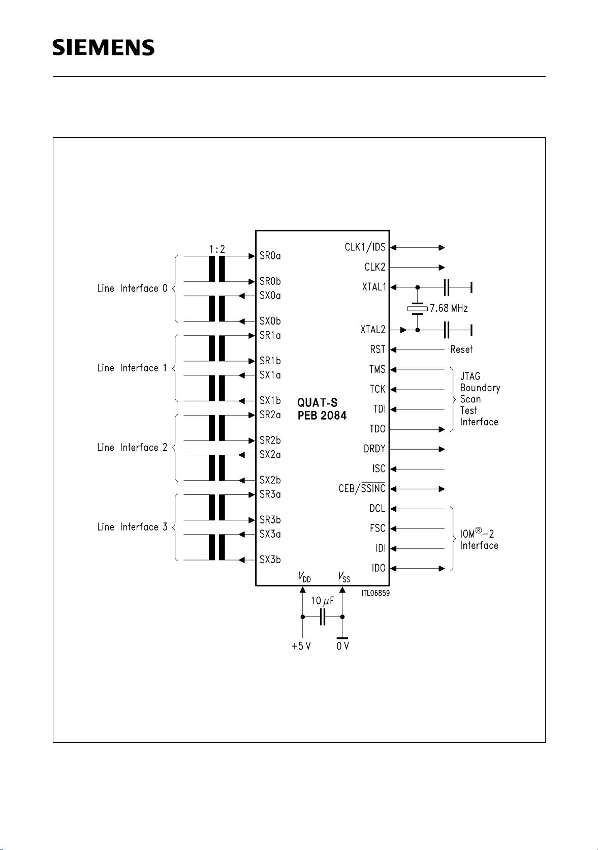
1.2 Logic Symbol
PEB 2084
Figure 1
QUAT-S Logic Symbol
Semiconductor Group 9
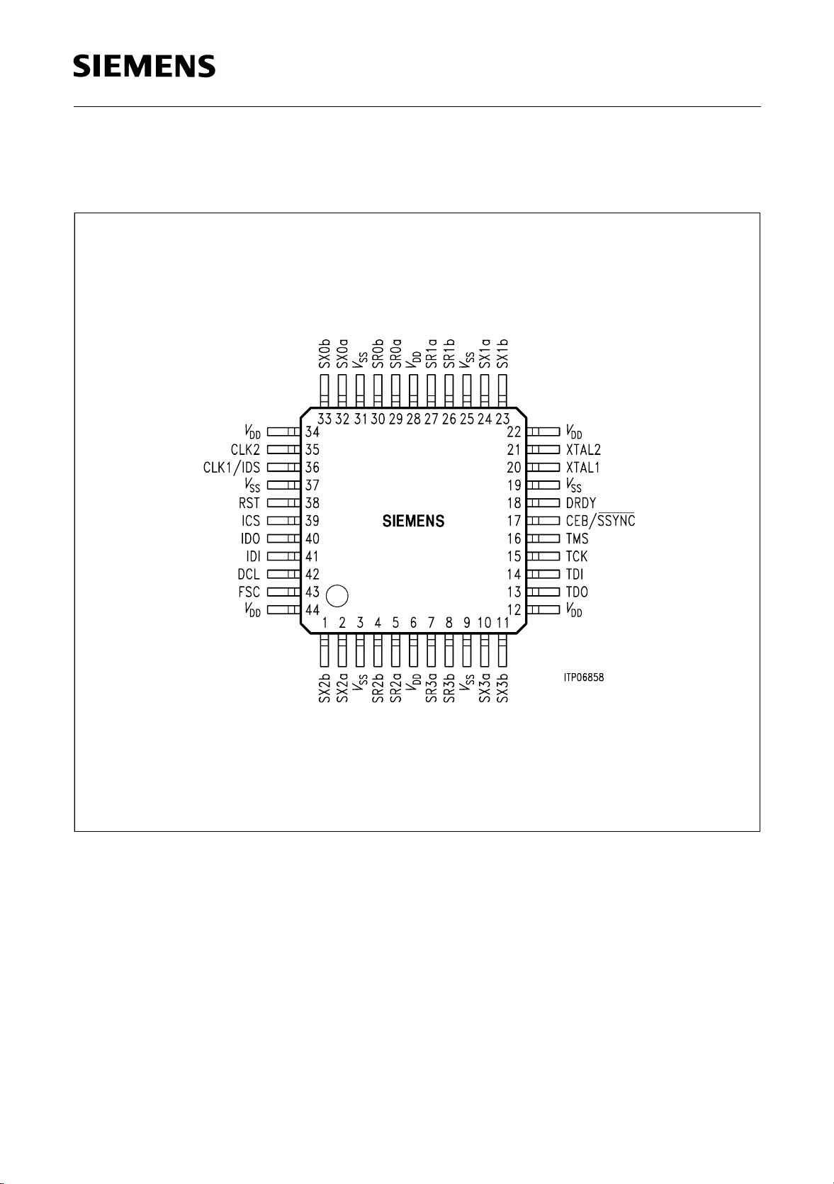
1.3 Pin Configuration
(top view)
PEB 2084
P-MQFP-44-2
Semiconductor Group 10

1.4 Pin Description
PEB 2084
Pin No. Symbol Input (I)
Output (O)
29, 30
32, 33
27, 26
24, 23
5, 4
2, 1
7, 8
10, 11
43
42
41
40
39
SR0a,b
SX0a,b
SR1a,b
SX1a,b
SR2a,b
SX2a,b
SR3a,b
SX3a,b
FSC
DCL
IDI
IDO
ICS
I
O
I
O
I
O
I
O
I
I
I
O/I
I
Function
S/T Interface a: positive, b: negative
No. 0: differential input
No. 0: differential output
No. 1: differential input
No. 1: differential output
No. 2: differential input
No. 2: differential output
No. 3: differential input
No. 3: differential output
®
-2 Interface
IOM
Frame Synchronization Clock (8 kHz)
Data Clock
IOM Interface Data Input: Data Downstream in LT-S
Data Upstream in LT-T
IOM Interface Data Output: Data Upstream in LT-S
Data Downstream in LT-T
Output
open-drain: resistor to
push-pull: resistor to V
V
SS
DD
resistor = 100 kΩ to 1 MΩ
refer to push-pull sensing, chapter 3.2
IOM Interface Channel Select (pin-strapping)
0: channels 0 though 3 selected
1: channels 4 through 7 selected
JTAG Boundary Scan Test Interface
16
15
14
13
20
21
Semiconductor Group 11
TMS
TCK
TDI
TDO
XTAL1
XTAL2
I
I
I
O
I
O
Test Mode Select
Test Clock 6.25 MHz
Test Data Input
Test Data Output
Oscillator or 7.68 MHz clock input
Oscillator output
1.4 Pin Description (cont’d)
PEB 2084
Pin No. Symbol Input (I)
Function
Output (O)
36 CLK1/
IDS
O/I CLK1: Clock output 1.536 MHz synchronized to
the trunk line (after reset in high impedance
state, only activated by programming
configuration regist er)
IDS: IOM-Interface Data Rate Select during HW
reset (pin-strapping)
0: double DCL (normal IOM-2 interface)
1: single DCL
The value of the input is sampled by the
falling edge of RST. Afterwards the pin may
be used for CLK1 functions.
35 CLK2 O 7.68 MHz clock output
38 RST I Reset, active high
17 CEB /
SSYNC
I/O /
I
CEB: Common echo bit for collision resolution in
logical subscriber LT-S bus configurations
(open drain output, external pull-up resistor
required.)
SSYNC
: Superframe synchronization input
18 DRDY O D-channel Ready signal to control HDLC hardware in
LT-T mode
(open-drain or push-pull operation identical to pin
IDO)
6, 12,
V
DD
I
+ 5 V power supply
22, 28,
34, 44
3, 9, 19,
V
SS
I
Reference ground
25, 31,
37
Semiconductor Group 12
PEB 2084
2 Functional Description
The PEB 2084, QUAT-S, performs the layer-1 functions of the ISDN basi c access for
four S/T interfaces.
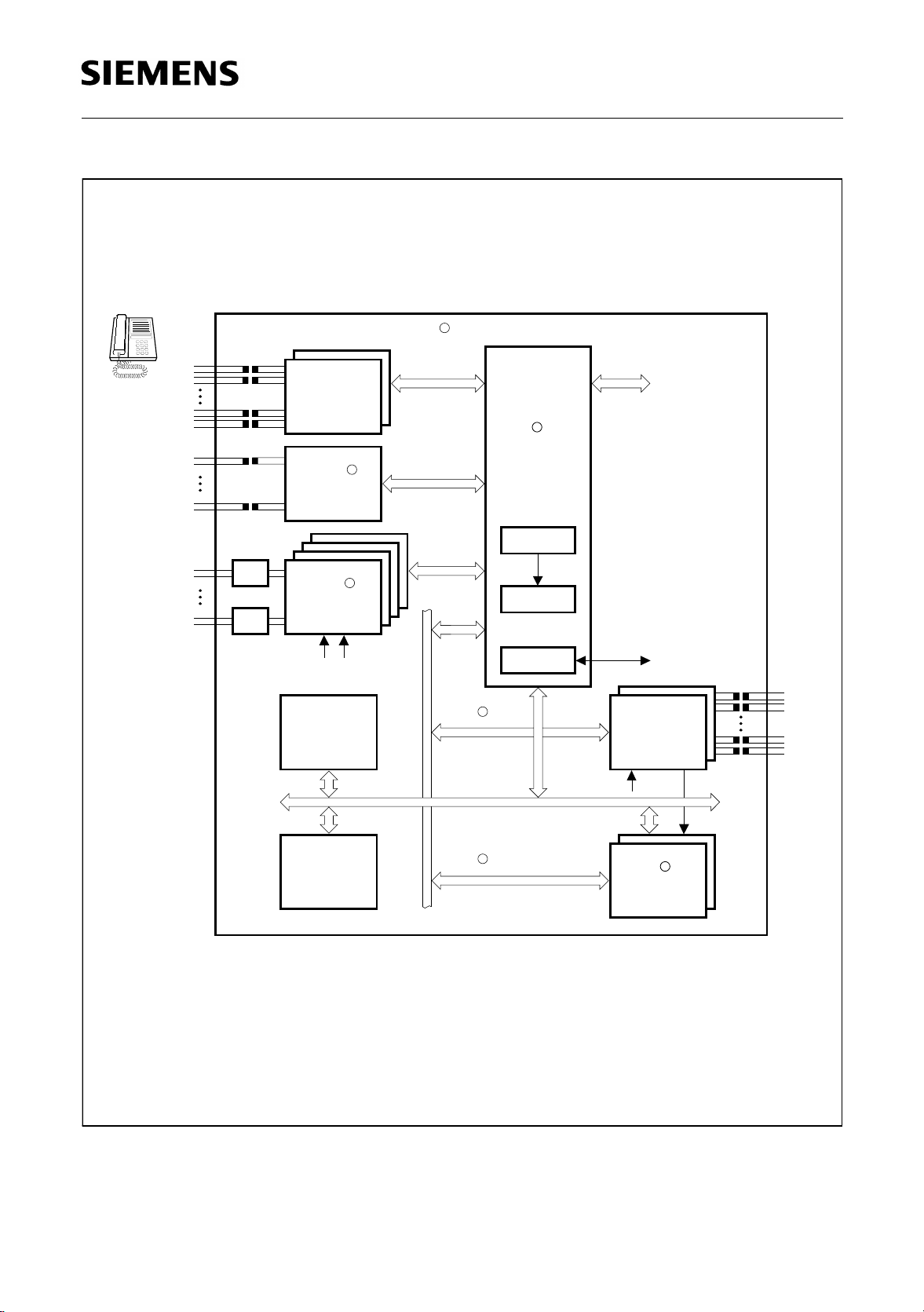
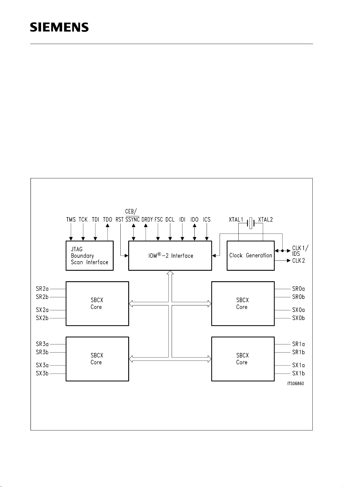
2.1 Device Architecture The QUAT-S contains the following functional blocks: Refer to figure 2
• Four line transceivers with analog S/T interfaces
• One digital IOM-2 interface
• Frame structure converter between the IOM-2 interface and the S/T interfaces
• JTAG boundary scan test interface
• Clocking, reset and initialization block
Figure 2
QUAT-S Device Architecture
Semiconductor Group 13
PEB 2084
2.2 Interfaces
PEB 2084, QUAT-S, provides four independent S/T interfaces, one IOM-2 interface and
one JTAG boundary scan test interface.
2.2.1 S/T Interface
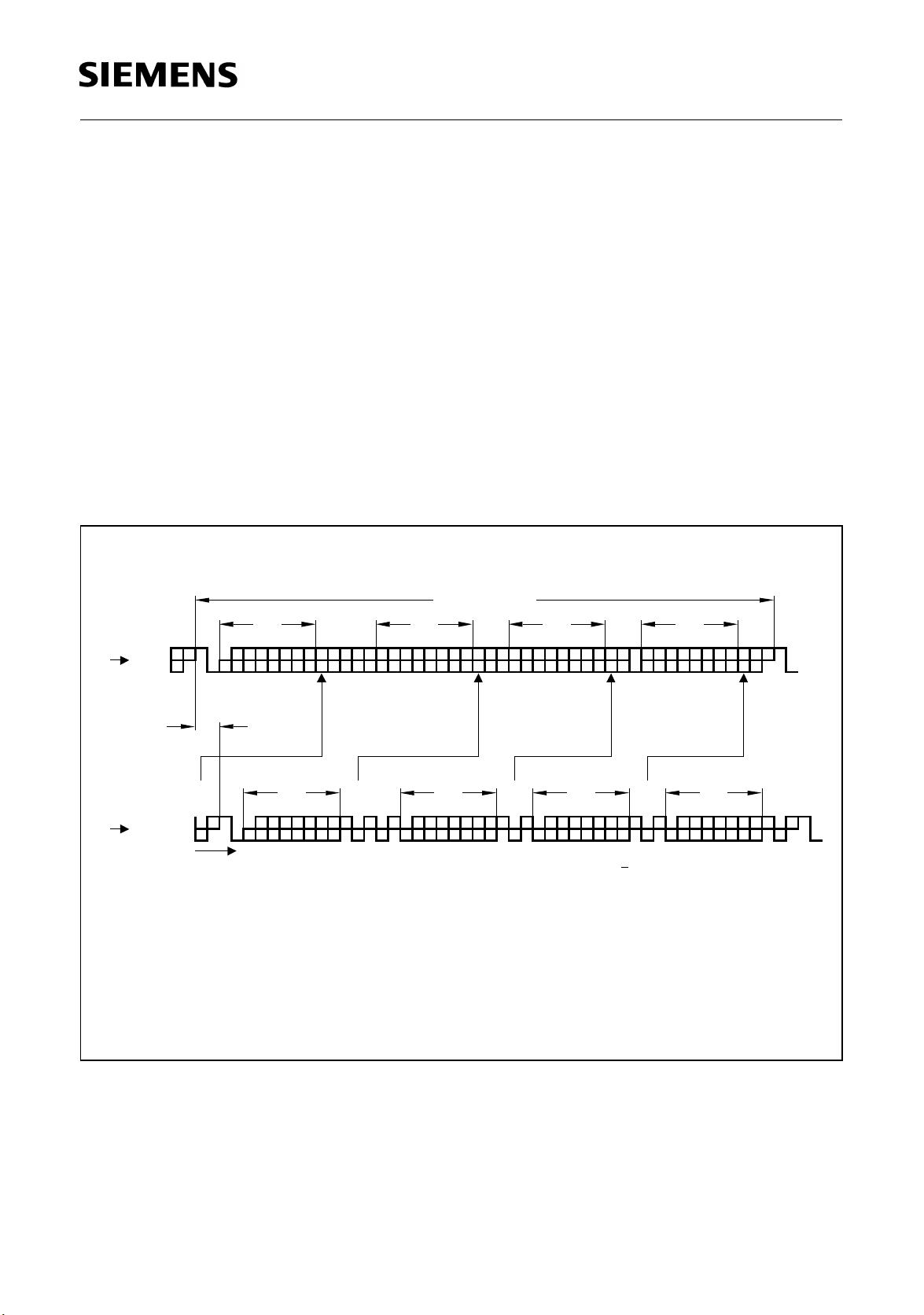
Frame Structure
One frame consists of 48 bits, at a nominal bit rate of 192 kbit/s. Thus each frame carries
two octets of B1, two octets of B2 and 4 bits of D-channel, according to the B1+B2+D
structure defined for the ISDN basic access (the total user data rate is 144 kbit/s). The
beginning of the frame is marked with a F-bit using a code violation (no Mark inversion).
The frame structures for data downstream (from network to subscriber) and for data
upstream (from subscriber to network) are shown in figure 3.
NT TE
NTTE
DL.
L.F B1 EDAF N
0
1
0
2 Bits Offset
0
1
0
F = Framing Bit
DC Balancing Bit=L
D-Channel Bit=D
D-Echo-Channel Bit=E
Auxiliary Framing Bit or Q-Bit=F
A
48 Bits in 250 µs
A
B2 EDM B1 SDEB2E D L. F L.
L.FL.DL.B1FL.L.D
A
L.FL.DL.B2L.D L.B1L.DL.B2
t
Bit set to a Binary Value N=N
B1 = Bit within B Channel
Bit within B Channel
B2 =
A = Bit used for Activation
S = Subchannel SC1 through SC5 bit position
M = Multiframing Bit
FA=
1
2
ITD02330
Figure 3
Frame Structure at Reference Points S and T (CCITT I.430)
The E-bit (= Echo bit to the D-channel bit) can be controlled via C/I channel and may be
used to carry the “available” / “blocked” information sent by ELIC, PEB 20550. Refer to
chapter 3.3.3.
Semiconductor Group 14
PEB 2084
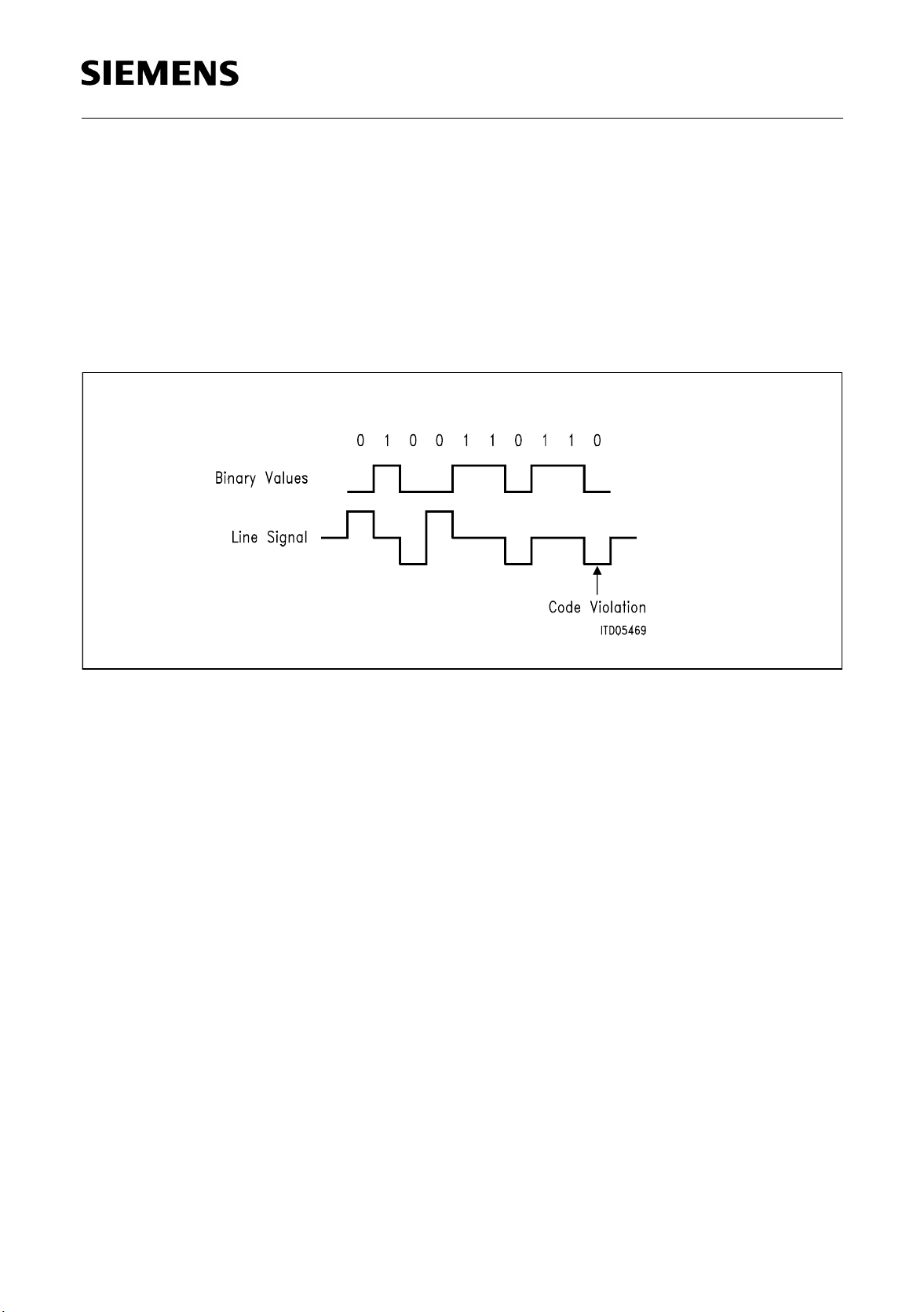
Coding
The QUAT-S uses a pseudo-ternary coding technique on the S/T interface (with a 100%
pulse width) according to CCITT I.430 reco mmendation. A binary ‘1’ corresponds to a
neutral level (space = no current) on the S/T line, binary ‘0’ s are coded as alternating
positive and negative pulses (= marks), figure 4.
Code violation (CV) is caused by two successive pulses with the same pola rity (= no
mark inversion).
Figure 4
S/T Interface Line Code
For details refer to Technical Manual PEB 2081, SBCX.
Semiconductor Group 15
PEB 2084
Interface Configurations
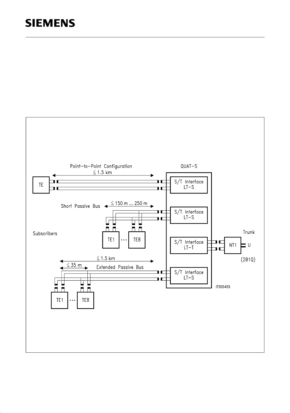
The QUAT-S provides four S/T interfaces for different applications, see figure 5:
• Subscriber’s connection to PBX (LT-S Mode) for different line configurations:
– Point-to-point
– Short passive bus
– Extended passive bus
• PBX connection to CO trunk (LT-T Mode)
Figure 5
S/T Interface Configurations
The T interface is physically identical to the S interface.
Semiconductor Group 16
PEB 2084
2.2.2 IOM®-2 System Interface
The PEB 2084, QUAT-S, is equipped with a digital ISDN Oriented Modular (IOM-2)
interface, for interconnection with other telecommunication ICs, such as IDEC
(PEB 2075), EPIC (PEB 2055) and EL IC (PEB 20550). EPIC and ELIC represent the
first switching stage towards the exchange system.
Figure 6
System Integration, IOM
®
-2 Interface
Interface Signals
The IOM-2 interface is a four-wire serial interfa ce which comprises two data lines and
two clock lines for synchronization. Refer to figure 6.
Data is carried over Data Upstream (DU) and Data Downstream (DD) lines. The
downstream and upstream directions are always seen with respect to the exchange.
Downstream refers to the information flow from the central exchange via PBX to the
subscriber and upstream vice versa.
Semiconductor Group 17

PEB 2084
Thus, depending on the programma ble QUAT-S mode, the data lines IDI and IDO get
different meanings: IDI (IOM interface Data Input) = Data Downstream in LT-S
= Data Upstream in LT-T
IDO (IOM-2 interface Data Output) = Data Upstream in LT-S
= Data Downstream in LT-T
The data is clocked by Data Clock (DCL) that operates at single or double data rate. The
selection is done by pinstrapping (CLK1/IDS). The IOM frames are delimited by an 8 kHz
Frame Synchronization Clock (FSC). The FSC rising edge indicates the start of an
-2 frame.
IOM
The IOM-2 interface speci fication desc ribes open drain d ata lines with ext ernal pull-up
resistors. However, if operation is logically point-to-point, tristate operation is possible as
well.
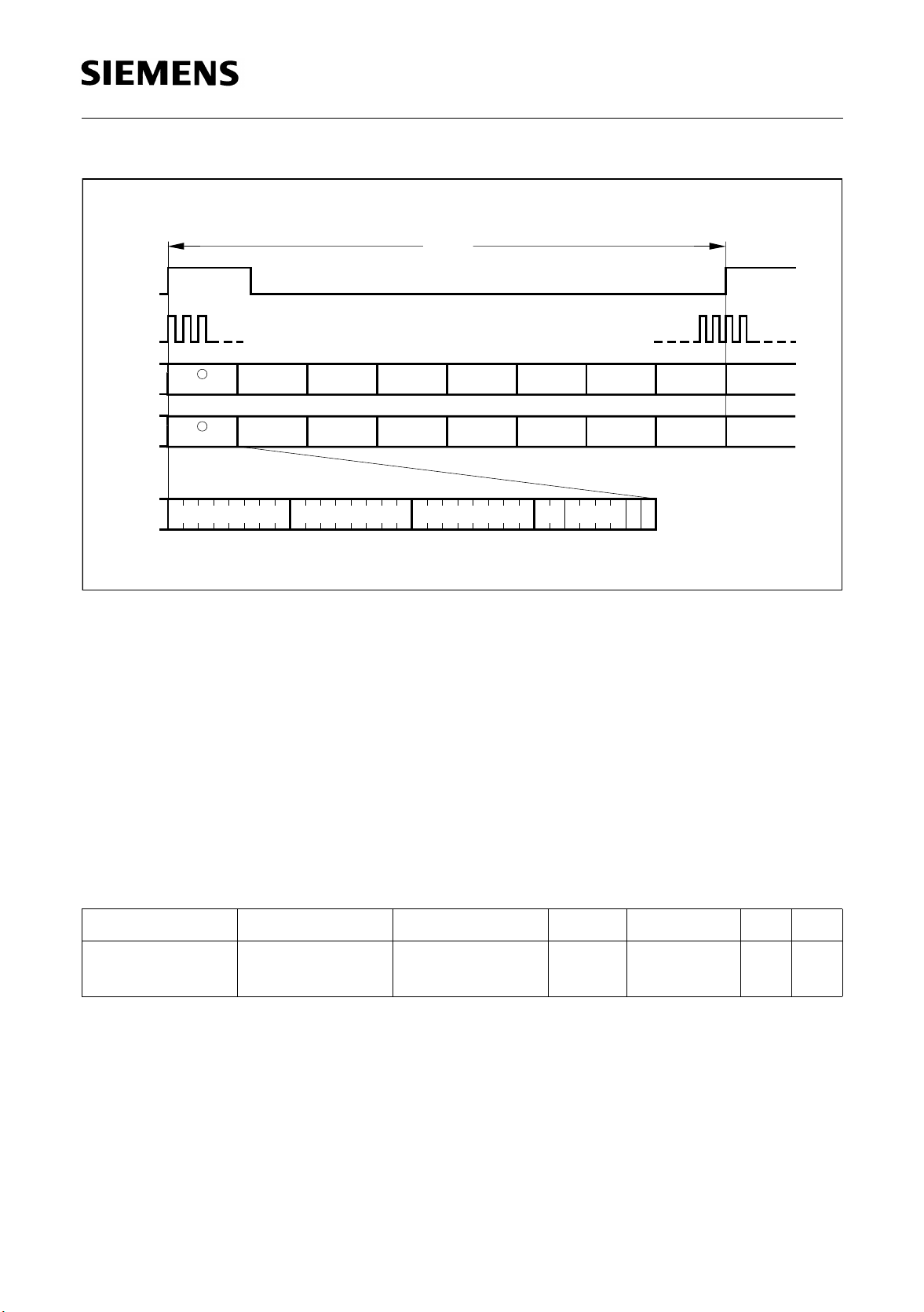
Frame Structure
One IOM-2 frame typically contains 8 IOM channels (sub-frames). The ISDN user data
rate is 144 kbit/s (B1 + B2 + D). The data is transmitted transparently synchronously and
in phase in both directions over the IOM-2 interface using time division multiplexing
within the 125 µs IOM-2 interface frame.
Refer to figure 7.
QUAT-S requires IOM-2 frame consisting of n complete ISDN channels (with 32 bits per
channel); n = 4, 5, 6, … 16.
Nominal bit rate of data (IDI and IDO) 1024 kbit/s … 4096 kbit/s
Nominal frequency of DCL 2048 kHz … 8192 kHz
Selectable frequency of DCL 1024 kHz … 4096 kHz
Nominal frequency of FSC 8 kHz
Semiconductor Group 18
PEB 2084
s
µ
125
FSC
DCL
R
IOM
DU
DD
CH0 CH1 CH2 CH3 CH4 CH5 CH6 CH7
R
IOM
CH7CH6CH5CH4CH3CH2CH1CH0
CH0
CH0
B1 B2
MONITOR
D
C/I
MM
RX
ITD04319
Figure 7
Multiplexed Frame Structure of the IOM-2 Interface in LT Mode with 2048 kbit/s
Data Rate
Each IOM ISDN channel consists of a total of 32 bits, or four octets:
B1 (8 bits) + B2 (8 bits) + D (2 bits) plus 14 bits for intercommunication.
• Two 8-bit B1 an d B2 channels fo r voice and data communicatio n with a data rat e of
64 kbit/s each,
• One 8-bit monitor channel for transferring maintenance information,
• One 2-bit D-channel for data transfer (e.g. signalling) with a data rate of 16 kbit/s
• Four command/indication (C/I) bits for controlling layer-1 functions.
• Two bits for handling the monitor channel: MR an MX (hand shake control).
8 bits 8 bits 8 bits 2 4 bits 1 1
B1 channel B2 channel Monitor channel D ch. Command/
MR MX
Indication
The user data rate is 144 kbit/s (B1 + B2 + D).
Monitor Channels
The monitor channel is used to convey message oriented local functions such as
software programming or access to internal registers via a layer-2 controller (ICC,
ELIC,…). There is a defined handshake procedure between the monitor channel
transmitter and the receiver in order to ensure a safe data transfer over the IOM-2
interface.
Semiconductor Group 19

PEB 2084
The monitor channel operates on an asynchronous basis. While data transfer on the bus
takes place synchronized to the frame, the data flow is controlled by a handshake
procedure using the monitor chann el rec eiv e bit (MR ) an d the m onitor channel transmit
bit (MX). For example: data is placed onto the monitor channel and the MX bit is
activated (active low). This data will be transmitted repeatedly once per 8 kHz frame until
the transfer is acknowledged via the MR bit.
The monitor channel is in an idle con dition when the MX bit is inactive in two or more
consecutive frames (indication of End Of Message EOM).
The monitor channel is also used to convey S and Q maintenance bits information (S/Q
channel).
The PEB 2084, QUAT-S, handles four monitor channels allocated to its four S/T
interfaces. The implemented monitor protocol is according to the IOM Interface
Specification, Rev. 2. For more details and an example refer to chapter 3.3.2.
D-Channels
The D-channels are sw itched transparently bet ween the S/T interf aces and the IOM-2
interface. Depending on the data load on a line card, different PBX architectures can be
implemented for D-channel handling in LT-S applications:
For decentral signalling, up to 32 subscribers can be served with only one special HDLC
controller which is integrated in the PEB 20550, ELIC (SACCO-A).
For intensive data packet handling in LT-S mode (e.g. in PC networks) or in LT-T
applications, additional HDLC controllers such as HSCX, IDEC, ESCC 2 or 8 or
MUNICH 32 may be connected to the IOM-2 interface. If a D-channel collision resolution
according to CCITT I.430 is require d, the QUAT-S o ffers a stro be signal to control the
connected HDLC (LAPD) controller.
For operational description refer to chapter 3.3.3.
C/I-Channels
A C/I-channel is used for communication between the PEB 2084, QUAT-S, and a
processor via a layer-2 device, to control and monitor layer-1 functions
(activation/deactivation and additional control functions). The layer-2 device monitors
the layer-1 indication continu ously and i ndicates a c hange i f a new code is found t o be
valid in two consecutive IOM frames (double last look criterion).
The codes originated by layer-2 devices are called “Commands”, those originated by the
PEB 2084, QUAT-S, are called “Indications”.
The PEB 2084, QUAT-S, handles four C/I-channels; one for each S/T transceiver.
For a list of the C/I codes and their use refer to chapter 3.6.
Semiconductor Group 20
PEB 2084
2.2.3 JTAG Boundary Scan Test Interface
The QUAT-S provides a boundary scan support for a cost effective board testing. It
consists of:
– Complete boundary scan for 11 signals (pins) according to IEEE Std. 1149.1
specification
– Test access port controller (TAP)
– Four dedicated pins (TCK, TMS, TDI, TDO)
– One 32-bit IDCODE register
– Specific functions for SXna,b
Boundary Scan
The following QUAT-S pins are included in the boundary scan:
FSC, DCL, IDI, IDO, RST, ICS, CEB, DRDY, CLK1, CLK2 and XTAL1.
Depending on the pin functionality one or two boundary scan cells are provided.
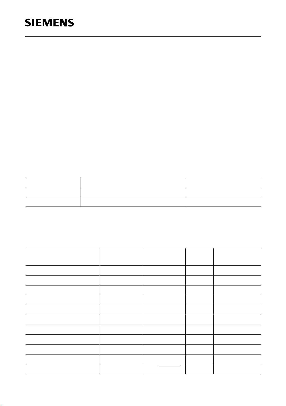
Pin Type Number of Boundary Scan Cells Usage
Input 1 Input
Output 2 Output, enable
When the TAP controller is in the appropriate mode data is shifted into/ out of the
boundary scan via the pins TDI/TDO using the 6.25 MHz clock on pin TCK.
The QUAT-S pins are included in the boundary scan in the following sequence:
Boundary Scan Number
TDI ––>
Pin Number Pin Name Type Number of
Scan Cells
143FSCI1
242DCLI1
341IDII1
440IDOO2+1
539ICSI1
638RSTI1
7 36 CLK1/IDS O/I 2 + 1
835CLK2O2
920XTAL1I1
10 18 DRDY O 2
11 17 CEB/SSYNC
Semiconductor Group 21
I/O 1 + 2

PEB 2084
TAP Controller
The Test Access Port (TAP) controller implements the state machine defined in the
JTAG standard IEEE Std. 1149.1. Transitions on the pin TMS cause the TAP contro lle r
to perform a state change.
Following the standard definition five instructions are executable.
TAP controller instructions:
Code Instruction Function
0000 EXTEST External testing
0001 INTEST Internal testing
0010 SAMPLE/PRELOAD Snap-shot testing
0011 IDCODE Reading ID code
0100 Test Mode TM1 Single pulses (2 kHz) on SXna,b
0101 Test Mode TM2 Continuous pulses (96 kHz) on SXna,b
11XX BYPASS Bypass operation
Note:The instructions TM1 and TM2 require 7.68 MHz at XTAL1.
EXTEST is used to examine the board interconnections.
When the TAP controller is in the state “update DR”, all output pins are updated with the
falling edge of TCK. When it has ente red state “capt ure DR” the levels of al l input pins
are latched with the rising edge of TCK. The in/out shifting of the scan vectors is typically
done using the instruction SAMPLE/PRELOAD.
INTEST supports internal chip testing.
When the TAP controller is in the state “update DR”, all inputs are updated internally with
the falling edge of TCK. When it has entered state “capture DR” the levels of all outputs
are latched with the rising edge of TCK. The in/out shifting of the scan vectors is typically
done using the instruction SAMPLE/PRELOAD.
0001 (INTEST) is the default value of the instruction register.
SAMPLE / PRELOAD provides a snap-shot of the pin level during norma l operation or
is used to preload (TDI) / shift out (TDO) the boundary scan with a test vector. Both
activities are transparent to the system functionality.
Note:The input pin XTAL1 should not be evaluated.
The input frequency (7.68 MHz) is not synchronous to TCK (6.25 MHz) which may
cause not predictable snap-shots on the pin XTAL1.
Semiconductor Group 22
 Loading...