

Siemens PEB20534 Datasheet

ICs for Communications
DMA Supported Serial Communication Controller with 4 Channels
DSCC4
PEB 20534 Version 2.0
Data Sheet 09.98
DS 2

PEB 20534
Revision History: Current Version: 09.98
Previous Version: Data Sheet 07.97 (V 1.1)
Page
(in previous
Version)
Page
(in current
Version)
Subjects (major changes since last revision)
- - This Data Sheet is completely reorganized.
For questions on technology, delivery and prices please contact the Semiconductor
Group Offices in Germany or the Siemens Companies and Representatives worldwide:
see our webpage at http://www.siemens.de/semiconductor/communication.
IOM®, IOM®-1, IOM®-2, SICOFI®, SICOFI®-2, SICOFI®-4, SICOFI®-4µC, SLICOFI®, ARCOFI
ARCOFI
SICAT
MUSAC
All other brand or product names, Hardware or Software names are trademarks or registered trademarks of their
respective companies or organizations.
®
-SP, EPIC®-1, EPIC®-S, ELIC®, IPAT®-2, ITAC®, ISAC®-S, ISAC®-S TE, ISAC®-P, ISAC®-P TE, IDEC®,
®
, OCTAT®-P, QUAT®-S are registered trademarks of Siem ens AG.
™
-A, FALC™54, IWE™, SARE™, UTPT™, ASM™, ASP™, DigiTape™ are trademarks of Siemens AG.
®
, ARCOFI®-BA,
Edition 09.98
Published by Siemens AG,
HL SC,
Balanstraße 73,
81541 München
© Siemens AG 1998.
All Rights Reserved.
Attention please!
As far as patents or other rights of third parties are concerned, liability is only assumed for components, not for
applications, processes and c irc uit s imp lemented within componen ts or as s em blies.
The information describe s the t yp e of co m ponent and shall not be considered as assured characteristics.
Terms of delivery and rights to ch ange design reserved.
Due to technical requireme nt s com ponents may contain dange rous substances. For informatio n on t he t y pes in
question please contact yo ur nearest Siemens Office, Semic onductor Group.
Siemens AG is an approved CECC manufacturer.
Packing
Please use the recycling ope rat ors k now n t o y ou. W e ca n als o help you – get in touch with your neares t sa les
office. By agreement we will take packing material back, if it is sorted. You must bear the costs of transport.
For packing material that is returned to us unsorted or which we are not obliged to accept, we shall have to invoice
you for any costs incurred.
Components used in life-support devices or systems must be expressly authorized for such purpose!
Critical components
systems
1 A critical component is a component used in a life-support device or system whose failure can reasonably be
2 Life support devices or systems are intended (a) to be implanted in the human body, or (b) to support and/or
2
with the express written approv al of the Semiconductor Group of Siem ens AG.
expected to cause the failure of that life-support device or system, or to affect its safety or effectiveness of that
device or system.
maintain and sustain human life. If th ey fail, it is rea so nable to assume that the health of th e us er m ay be endangered.
1
of the Semiconductor Group of Siemens AG, may only be used in life -s upport devices or

PEB 20534
Preface
The
DMA Supported Serial Commu nication Controller with 4 Channels
Multi Protocol Controller for a wide range of data communication and telecommunication
applications. This docume nt provi des co mplete refere nce inf ormation on hard ware an d
software related issues as well as on general operation.
Organization of this Document
This Data Sheet is divided into 16 chapters. It is organized as follows:
• Chapter 1, Overview
Gives a general description of the product, lists the key features, and prese nts som e
typical applications.
• Chapter 2, Pin Description
Lists pin locations wi th associ ated sign als , categoriz es signal s acc ording to func tion,
and describes signals.
(DSCC4) is a
• Chapters 3,4,5,6,7 Functional Description
These chapters provide detailed descriptions of all DSCC4 internal function blocks.
• Chapter 8, Detailed Protocol Descriptions
Gives a detailed d escription of all protocols s upported by the serial communic ation
controllers SCCs.
• Chapter 9, Reset and Initializat ion Pro ced ure
Gives examples for DSCC4 initialization procedure and operation.
• Chapter 10, Detailed Register Description
Gives a detailed description of all DSCC4 on chip registers.
• Chapter 11, Host Memory Organization
Provides an overview of all DSCC4 data structures located in the shared memory
• Chapter 12, JTAG Boundary Scan
Gives a detailed description of the boundary scan unit.
• Chapter 13 Application Examples
These chapters will provide additional information on special applications and bus
utilization analysis.
• Chapter 14, Electrical Characteristics
Gives a detailed de scription of all electrical DC and AC c haracteri stics and prov ides
Semiconductor Group 3 Data Sheet 09.98

timing diagrams and values for all interfaces.
• Chapter 15, Package Outline
PEB 20534
Semiconductor Group 4 Data Sheet 09.98

PEB 20534
Table of Contents Page
1 Overview . . . . . . . . . . . . . . . . . . . . . . . . . . . . . . . . . . . . . . . . . . . . . . . . . . .18
1.1 Features . . . . . . . . . . . . . . . . . . . . . . . . . . . . . . . . . . . . . . . . . . . . . . . . . . . .19
1.2 Differences Between the DSCC4 and the ESCC Family . . . . . . . . . . . . . . .22
1.2.1 Enhancements to the ESCC Serial Core . . . . . . . . . . . . . . . . . . . . . . . . .22
1.2.2 Simplifications to the ESCC Serial Core . . . . . . . . . . . . . . . . . . . . . . . . .22
1.3 Logic Symbol . . . . . . . . . . . . . . . . . . . . . . . . . . . . . . . . . . . . . . . . . . . . . . . .23
1.4 Typical Applications . . . . . . . . . . . . . . . . . . . . . . . . . . . . . . . . . . . . . . . . . . .24
1.4.1 Application Examples . . . . . . . . . . . . . . . . . . . . . . . . . . . . . . . . . . . . . . .26
1.4.1.1 HSSI Application . . . . . . . . . . . . . . . . . . . . . . . . . . . . . . . . . . . . . . . . .26
1.4.1.2 HSSI Application . . . . . . . . . . . . . . . . . . . . . . . . . . . . . . . . . . . . . . . . .27
1.4.1.3 General Data Application . . . . . . . . . . . . . . . . . . . . . . . . . . . . . . . . . . .28
2 Pin Descriptions . . . . . . . . . . . . . . . . . . . . . . . . . . . . . . . . . . . . . . . . . . . . .29
2.1 Pin Diagram . . . . . . . . . . . . . . . . . . . . . . . . . . . . . . . . . . . . . . . . . . . . . . . . .29
2.2 Pin Definitions and Functions . . . . . . . . . . . . . . . . . . . . . . . . . . . . . . . . . . .30
3 Functional Description. . . . . . . . . . . . . . . . . . . . . . . . . . . . . . . . . . . . . . . .48
4 Microprocessor Bus Interface. . . . . . . . . . . . . . . . . . . . . . . . . . . . . . . . . .51
4.1 PCI Bus Interface . . . . . . . . . . . . . . . . . . . . . . . . . . . . . . . . . . . . . . . . . . . . .51
4.1.1 Supported PCI Transactions . . . . . . . . . . . . . . . . . . . . . . . . . . . . . . . . . .51
4.1.2 PCI Configuration Space Register Overview . . . . . . . . . . . . . . . . . . . . . .52
4.2 De-multiplexed Bus Interface Extension . . . . . . . . . . . . . . . . . . . . . . . . . . .53
5 DMA Controller and Central FIFOs . . . . . . . . . . . . . . . . . . . . . . . . . . . . . .57
5.1 DMAC Operational Description . . . . . . . . . . . . . . . . . . . . . . . . . . . . . . . . . .59
5.1.1 DMAC Register Overview . . . . . . . . . . . . . . . . . . . . . . . . . . . . . . . . . . . .59
5.1.2 DMAC Control and Data Structures . . . . . . . . . . . . . . . . . . . . . . . . . . . . .64
5.1.2.1 DMAC Transmit Descriptor Lists . . . . . . . . . . . . . . . . . . . . . . . . . . . . .66
5.1.2.2 DMAC Receive Descriptor Lists . . . . . . . . . . . . . . . . . . . . . . . . . . . . .71
5.1.2.3 DMAC Operation Using Hold-Bit Control Mechanism . . . . . . . . . . . . .76
5.1.2.4 DMAC Operation Using Last Descriptor Address Control Mode . . . . .78
5.1.3 DMAC Interrupt Controller . . . . . . . . . . . . . . . . . . . . . . . . . . . . . . . . . . . .81
5.2 Central FIFOs Operational Description . . . . . . . . . . . . . . . . . . . . . . . . . . . .85
5.2.1 Central FIFO Register Overview . . . . . . . . . . . . . . . . . . . . . . . . . . . . . . .85
5.2.2 Central Transmit FIFO (TFIFO) . . . . . . . . . . . . . . . . . . . . . . . . . . . . . . . .89
5.2.3 Central Receive FIFO (RFIFO) . . . . . . . . . . . . . . . . . . . . . . . . . . . . . . . .92
5.2.4 DMAC Internal Arbitration Scheme . . . . . . . . . . . . . . . . . . . . . . . . . . . . .93
5.2.5 DMAC Performance . . . . . . . . . . . . . . . . . . . . . . . . . . . . . . . . . . . . . . . . .94
5.2.6 Little / Big Endian Byte Swap Convention . . . . . . . . . . . . . . . . . . . . . . . .95
6 Multi Function Port (MFP) . . . . . . . . . . . . . . . . . . . . . . . . . . . . . . . . . . . . .96
6.1 Local Bus Interface (LBI) . . . . . . . . . . . . . . . . . . . . . . . . . . . . . . . . . . . . . . .98
Semiconductor Group 5 Data Sheet 09.98

PEB 20534
6.1.1 LBI Bus Modes . . . . . . . . . . . . . . . . . . . . . . . . . . . . . . . . . . . . . . . . . . . .99
6.1.1.1 LBI External Bus Controller (EBC) . . . . . . . . . . . . . . . . . . . . . . . . . . .99
6.1.1.2 Multiplexed Local Bus Modes . . . . . . . . . . . . . . . . . . . . . . . . . . . . . . .99
6.1.1.3 De-multiplexed Local Bus Modes . . . . . . . . . . . . . . . . . . . . . . . . . . .100
6.1.1.4 Programmable Bus Characteristics . . . . . . . . . . . . . . . . . . . . . . . . . .102
6.1.1.5 Ready Signal Controlled Bus Cycles . . . . . . . . . . . . . . . . . . . . . . . . .104
6.1.1.6 LBI (EBC) Configuration . . . . . . . . . . . . . . . . . . . . . . . . . . . . . . . . . .106
6.1.2 LBI Bus Arbitration . . . . . . . . . . . . . . . . . . . . . . . . . . . . . . . . . . . . . . . . .107
6.1.3 PCI to Local Bus Bridge Operation . . . . . . . . . . . . . . . . . . . . . . . . . . . .113
6.1.4 LBI Interrupt Generation . . . . . . . . . . . . . . . . . . . . . . . . . . . . . . . . . . . .114
6.2 Synchronous Serial Control (SSC) Interface . . . . . . . . . . . . . . . . . . . . . . .115
6.2.1 SSC Functional Description . . . . . . . . . . . . . . . . . . . . . . . . . . . . . . . . . .115
6.2.1.1 Overview . . . . . . . . . . . . . . . . . . . . . . . . . . . . . . . . . . . . . . . . . . . . . .115
6.2.1.2 Operational Mode: Full-Duplex Operation: . . . . . . . . . . . . . . . . . . . .119
6.2.1.3 Operational Mode: Half Duplex Operation: . . . . . . . . . . . . . . . . . . . .122
6.2.1.4 Baud Rate Generation . . . . . . . . . . . . . . . . . . . . . . . . . . . . . . . . . . . .124
6.2.1.5 Error Detection . . . . . . . . . . . . . . . . . . . . . . . . . . . . . . . . . . . . . . . . .124
6.2.2 SSC Interrupt (Vector) . . . . . . . . . . . . . . . . . . . . . . . . . . . . . . . . . . . . . .126
6.3 General Purpose Port (GPP) Interface . . . . . . . . . . . . . . . . . . . . . . . . . . .127
6.3.1 GPP Functional Description . . . . . . . . . . . . . . . . . . . . . . . . . . . . . . . . .127
6.3.2 GPP Interrupt Vector . . . . . . . . . . . . . . . . . . . . . . . . . . . . . . . . . . . . . . .127
7 Serial Communication Controller (SCC) Cores . . . . . . . . . . . . . . . . . . .128
7.1 General . . . . . . . . . . . . . . . . . . . . . . . . . . . . . . . . . . . . . . . . . . . . . . . . . . .128
7.2 Protocol Modes Overview . . . . . . . . . . . . . . . . . . . . . . . . . . . . . . . . . . . . .132
7.3 SCC FIFOs . . . . . . . . . . . . . . . . . . . . . . . . . . . . . . . . . . . . . . . . . . . . . . . .133
7.3.1 SCC Transmit FIFO . . . . . . . . . . . . . . . . . . . . . . . . . . . . . . . . . . . . . . . .133
7.3.2 SCC Receive FIFO . . . . . . . . . . . . . . . . . . . . . . . . . . . . . . . . . . . . . . . .134
7.4 Clocking System . . . . . . . . . . . . . . . . . . . . . . . . . . . . . . . . . . . . . . . . . . . .137
7.4.1 Clock Modes . . . . . . . . . . . . . . . . . . . . . . . . . . . . . . . . . . . . . . . . . . . . .141
7.4.1.1 Clock Mode 0 (0a/0b) . . . . . . . . . . . . . . . . . . . . . . . . . . . . . . . . . . . .141
7.4.1.2 Clock Mode 1 . . . . . . . . . . . . . . . . . . . . . . . . . . . . . . . . . . . . . . . . . . .142
7.4.1.3 Clock Mode 2 (2a/2b) . . . . . . . . . . . . . . . . . . . . . . . . . . . . . . . . . . . .143
7.4.1.4 Clock Mode 3 (3a/3b) . . . . . . . . . . . . . . . . . . . . . . . . . . . . . . . . . . . .144
7.4.1.5 Clock Mode 4 (High Speed Interface Clock Mode) . . . . . . . . . . . . . .145
7.4.1.6 Clock Mode 5 . . . . . . . . . . . . . . . . . . . . . . . . . . . . . . . . . . . . . . . . . . .147
7.4.1.7 Clock Mode 6 (6a/6b) . . . . . . . . . . . . . . . . . . . . . . . . . . . . . . . . . . . .152
7.4.1.8 Clock Mode 7 (7a/7b) . . . . . . . . . . . . . . . . . . . . . . . . . . . . . . . . . . . .153
7.4.2 Baud Rate Generator (BRG) . . . . . . . . . . . . . . . . . . . . . . . . . . . . . . . . .154
7.4.3 Clock Recovery (DPLL) . . . . . . . . . . . . . . . . . . . . . . . . . . . . . . . . . . . . .155
7.5 SCC Interrupt Interface . . . . . . . . . . . . . . . . . . . . . . . . . . . . . . . . . . . . . . .158
7.6 High Speed Channel Operation (PEB 20534H-52 only) . . . . . . . . . . . . . .159
7.7 Serial Bus Configuration Mode . . . . . . . . . . . . . . . . . . . . . . . . . . . . . . . . .159
Semiconductor Group 6 Data Sheet 09.98

PEB 20534
7.7.1 Serial Bus Access Procedure . . . . . . . . . . . . . . . . . . . . . . . . . . . . . . . .160
7.7.2 Serial Bus Collisions and Recovery . . . . . . . . . . . . . . . . . . . . . . . . . . . .160
7.7.3 Serial Bus Access Priority Scheme . . . . . . . . . . . . . . . . . . . . . . . . . . . .161
7.7.4 Serial Bus Configuration Timing Modes . . . . . . . . . . . . . . . . . . . . . . . .161
7.7.5 Functions Of Signal RTS in HDLC Mode . . . . . . . . . . . . . . . . . . . . . . . .162
7.8 Data Encoding . . . . . . . . . . . . . . . . . . . . . . . . . . . . . . . . . . . . . . . . . . . . . .162
7.8.1 NRZ and NRZI Encoding . . . . . . . . . . . . . . . . . . . . . . . . . . . . . . . . . . . .162
7.8.2 FM0 and FM1 Encoding . . . . . . . . . . . . . . . . . . . . . . . . . . . . . . . . . . . .163
7.8.3 Manchester Encoding . . . . . . . . . . . . . . . . . . . . . . . . . . . . . . . . . . . . . .164
7.9 Modem Control Signals (RTS, CTS, CD) . . . . . . . . . . . . . . . . . . . . . . . . .164
7.9.1 RTS/CTS Handshaking . . . . . . . . . . . . . . . . . . . . . . . . . . . . . . . . . . . . .164
7.9.2 Carrier Detect (CD) Receiver Control . . . . . . . . . . . . . . . . . . . . . . . . . .166
7.10 Local Loop Test Mode . . . . . . . . . . . . . . . . . . . . . . . . . . . . . . . . . . . . . . . .166
8 Detailed Protocol Description . . . . . . . . . . . . . . . . . . . . . . . . . . . . . . . . .167
8.1 HDLC/SDLC Protocol Modes . . . . . . . . . . . . . . . . . . . . . . . . . . . . . . . . . .169
8.1.1 HDLC . . . . . . . . . . . . . . . . . . . . . . . . . . . . . . . . . . . . . . . . . . . . . . . . . . .169
8.1.1.1 Auto Mode . . . . . . . . . . . . . . . . . . . . . . . . . . . . . . . . . . . . . . . . . . . . .170
8.1.1.2 Non Auto Mode . . . . . . . . . . . . . . . . . . . . . . . . . . . . . . . . . . . . . . . . .170
8.1.1.3 Address Mode 1 . . . . . . . . . . . . . . . . . . . . . . . . . . . . . . . . . . . . . . . . .171
8.1.1.4 Address Mode 0 . . . . . . . . . . . . . . . . . . . . . . . . . . . . . . . . . . . . . . . . .171
8.1.2 HDLC/PPP Protocol Mode . . . . . . . . . . . . . . . . . . . . . . . . . . . . . . . . . . .171
8.1.2.1 Bit Synchronous PPP . . . . . . . . . . . . . . . . . . . . . . . . . . . . . . . . . . . .171
8.1.2.2 Octet Synchronous PPP . . . . . . . . . . . . . . . . . . . . . . . . . . . . . . . . . .172
8.1.2.3 Aynchronous PPP . . . . . . . . . . . . . . . . . . . . . . . . . . . . . . . . . . . . . . .172
8.1.3 Extended Transparent Mode . . . . . . . . . . . . . . . . . . . . . . . . . . . . . . . . .172
8.1.4 HDLC Receive Data Processing Overview . . . . . . . . . . . . . . . . . . . . . .172
8.1.5 HDLC Transmit Data Processing Overview . . . . . . . . . . . . . . . . . . . . . .174
8.1.6 Procedural Support (Layer-2 Functions) . . . . . . . . . . . . . . . . . . . . . . . .176
8.1.7 Full-Duplex LAPB/LAPD Operation . . . . . . . . . . . . . . . . . . . . . . . . . . . .177
8.1.8 Half-Duplex SDLC-NRM Operation . . . . . . . . . . . . . . . . . . . . . . . . . . . .182
8.1.9 Special Functions . . . . . . . . . . . . . . . . . . . . . . . . . . . . . . . . . . . . . . . . .185
8.1.9.1 Extended Transparent Transmission and Reception . . . . . . . . . . . . .185
8.1.9.2 Receive Address Handling . . . . . . . . . . . . . . . . . . . . . . . . . . . . . . . .185
8.1.9.3 Shared Flags . . . . . . . . . . . . . . . . . . . . . . . . . . . . . . . . . . . . . . . . . . .185
8.1.9.4 One Bit Insertion . . . . . . . . . . . . . . . . . . . . . . . . . . . . . . . . . . . . . . . .186
8.1.9.5 Preamble Transmission . . . . . . . . . . . . . . . . . . . . . . . . . . . . . . . . . . .186
8.1.9.6 CRC Generation and Checking . . . . . . . . . . . . . . . . . . . . . . . . . . . . .186
8.1.9.7 Data Transparency in PPP Mode . . . . . . . . . . . . . . . . . . . . . . . . . . .188
8.1.9.8 Receive Length Check Feature . . . . . . . . . . . . . . . . . . . . . . . . . . . . .190
8.2 Asynchronous (ASYNC) Protocol Mode . . . . . . . . . . . . . . . . . . . . . . . . . .191
8.2.1 Character Framing . . . . . . . . . . . . . . . . . . . . . . . . . . . . . . . . . . . . . . . . .191
8.2.2 Data Reception . . . . . . . . . . . . . . . . . . . . . . . . . . . . . . . . . . . . . . . . . . .191
Semiconductor Group 7 Data Sheet 09.98

PEB 20534
8.2.2.1 Asynchronous Mode . . . . . . . . . . . . . . . . . . . . . . . . . . . . . . . . . . . . .191
8.2.2.2 Isochronous Mode . . . . . . . . . . . . . . . . . . . . . . . . . . . . . . . . . . . . . . .192
8.2.2.3 Storage of Receive Data . . . . . . . . . . . . . . . . . . . . . . . . . . . . . . . . . .192
8.2.3 Data Transmission . . . . . . . . . . . . . . . . . . . . . . . . . . . . . . . . . . . . . . . . .193
8.2.4 Special Functions . . . . . . . . . . . . . . . . . . . . . . . . . . . . . . . . . . . . . . . . .193
8.2.4.1 Break Detection/Generation . . . . . . . . . . . . . . . . . . . . . . . . . . . . . . .193
8.2.4.2 In-band Flow Control by XON/XOFF Characters . . . . . . . . . . . . . . .193
8.2.4.3 Out-of-band Flow Control . . . . . . . . . . . . . . . . . . . . . . . . . . . . . . . . .195
8.3 Character Oriented Synchronous (BISYNC) Protocol Mode . . . . . . . . . . .198
8.3.1 Character Framing . . . . . . . . . . . . . . . . . . . . . . . . . . . . . . . . . . . . . . . . .198
8.3.2 Data Reception . . . . . . . . . . . . . . . . . . . . . . . . . . . . . . . . . . . . . . . . . . .198
8.3.3 Data Transmission . . . . . . . . . . . . . . . . . . . . . . . . . . . . . . . . . . . . . . . . .199
8.3.4 Special Functions . . . . . . . . . . . . . . . . . . . . . . . . . . . . . . . . . . . . . . . . .200
8.3.4.1 Preamble Transmission . . . . . . . . . . . . . . . . . . . . . . . . . . . . . . . . . . .200
8.3.4.2 CRC Parity Inhibit . . . . . . . . . . . . . . . . . . . . . . . . . . . . . . . . . . . . . . .200
9 Reset and Initialization Procedure . . . . . . . . . . . . . . . . . . . . . . . . . . . . .201
9.1 Reset and Power-On . . . . . . . . . . . . . . . . . . . . . . . . . . . . . . . . . . . . . . . . .201
9.2 Initialization Example . . . . . . . . . . . . . . . . . . . . . . . . . . . . . . . . . . . . . . . . .203
9.3 Start of Operation . . . . . . . . . . . . . . . . . . . . . . . . . . . . . . . . . . . . . . . . . . .207
9.4 Initialization Example . . . . . . . . . . . . . . . . . . . . . . . . . . . . . . . . . . . . . . . . .214
9.4.1 Test Loop For Data Transfer in HDLC Address Mode 0 . . . . . . . . . . . .214
10 Detailed Register Description . . . . . . . . . . . . . . . . . . . . . . . . . . . . . . . . .220
10.1 Register Range Overview and Address Mapping . . . . . . . . . . . . . . . . . . .221
10.2 PCI Configuration Space - Detailed Register Description . . . . . . . . . . . . .222
10.3 On-Chip Registers Description . . . . . . . . . . . . . . . . . . . . . . . . . . . . . . . . .228
10.3.1 Global Registers - Detailed Register Description . . . . . . . . . . . . . . . . .228
10.3.1.1 Global Registers Overview . . . . . . . . . . . . . . . . . . . . . . . . . . . . . . . .228
10.3.1.2 Global Registers Description . . . . . . . . . . . . . . . . . . . . . . . . . . . . . . .231
10.3.2 SCC Registers - Detailed Register Description . . . . . . . . . . . . . . . . . . .272
10.3.2.1 SCC Registers Overview . . . . . . . . . . . . . . . . . . . . . . . . . . . . . . . . . .272
10.3.2.2 SCC Registers Description . . . . . . . . . . . . . . . . . . . . . . . . . . . . . . . .274
10.3.3 Peripheral Registers - Detailed Register Description . . . . . . . . . . . . . .349
10.3.3.1 Peripheral Registers Overview . . . . . . . . . . . . . . . . . . . . . . . . . . . . .349
10.3.3.2 LBI Registers Description . . . . . . . . . . . . . . . . . . . . . . . . . . . . . . . . .351
10.3.3.3 SSC Registers Description . . . . . . . . . . . . . . . . . . . . . . . . . . . . . . . .355
10.3.3.4 GPP Registers Description . . . . . . . . . . . . . . . . . . . . . . . . . . . . . . . .368
11 Host Memory Organization . . . . . . . . . . . . . . . . . . . . . . . . . . . . . . . . . . .374
11.1 Linked List Structure . . . . . . . . . . . . . . . . . . . . . . . . . . . . . . . . . . . . . . . . .374
11.1.1 Transmit Descriptor Lists . . . . . . . . . . . . . . . . . . . . . . . . . . . . . . . . . . . .374
11.1.1.1 Transmit Descriptor . . . . . . . . . . . . . . . . . . . . . . . . . . . . . . . . . . . . . .374
Semiconductor Group 8 Data Sheet 09.98

PEB 20534
11.1.2 Receive Descriptor Lists . . . . . . . . . . . . . . . . . . . . . . . . . . . . . . . . . . . .378
11.1.2.1 Receive Descriptor . . . . . . . . . . . . . . . . . . . . . . . . . . . . . . . . . . . . . .379
11.1.2.2 Receive Data Section Status Byte (HDLC Mode) . . . . . . . . . . . . . . .383
11.1.2.3 Receive Data Section Status Byte (ASYNC/BISYNC Modes) . . . . . .386
11.2 Interrupt Queue Structure . . . . . . . . . . . . . . . . . . . . . . . . . . . . . . . . . . . . .387
11.2.1 Interrupt Queue Overview . . . . . . . . . . . . . . . . . . . . . . . . . . . . . . . . . . .387
11.2.2 Interrupt Vector Overview . . . . . . . . . . . . . . . . . . . . . . . . . . . . . . . . . . .389
11.2.2.1 Configuration Interrupt Vector . . . . . . . . . . . . . . . . . . . . . . . . . . . . . .390
11.2.2.2 DMA Controller Interrupt Vector . . . . . . . . . . . . . . . . . . . . . . . . . . . .391
11.2.2.3 SCC Interrupt Vector . . . . . . . . . . . . . . . . . . . . . . . . . . . . . . . . . . . . .393
11.2.2.4 SSC Interrupt Vector . . . . . . . . . . . . . . . . . . . . . . . . . . . . . . . . . . . . .395
11.2.2.5 LBI Interrupt Vector . . . . . . . . . . . . . . . . . . . . . . . . . . . . . . . . . . . . . .397
11.2.2.6 GPP Interrupt Vector . . . . . . . . . . . . . . . . . . . . . . . . . . . . . . . . . . . . .398
12 Test Configuration . . . . . . . . . . . . . . . . . . . . . . . . . . . . . . . . . . . . . . . . . .399
12.1 JTAG Boundary Scan Interface . . . . . . . . . . . . . . . . . . . . . . . . . . . . . . . . .399
13 Application Hints . . . . . . . . . . . . . . . . . . . . . . . . . . . . . . . . . . . . . . . . . . .406
13.1 DSCC4 PCI Bus Utilization . . . . . . . . . . . . . . . . . . . . . . . . . . . . . . . . . . . .406
13.2 Application Example: De-multiplexed Bus Interface . . . . . . . . . . . . . . . . .407
13.3 SSC Example: Connecting A Serial EEPROM . . . . . . . . . . . . . . . . . . . . .408
14 Electrical Characteristics. . . . . . . . . . . . . . . . . . . . . . . . . . . . . . . . . . . . .409
14.1 Important Electrical Requirements . . . . . . . . . . . . . . . . . . . . . . . . . . . . . . .409
14.2 Absolute Maximum Ratings . . . . . . . . . . . . . . . . . . . . . . . . . . . . . . . . . . . .411
14.3 Thermal Package Characteristics . . . . . . . . . . . . . . . . . . . . . . . . . . . . . . .411
14.4 DC Characteristics . . . . . . . . . . . . . . . . . . . . . . . . . . . . . . . . . . . . . . . . . . .412
14.5 Capacitances . . . . . . . . . . . . . . . . . . . . . . . . . . . . . . . . . . . . . . . . . . . . . . .413
14.6 AC Characteristics . . . . . . . . . . . . . . . . . . . . . . . . . . . . . . . . . . . . . . . . . . .414
14.6.1 PCI Bus Interface Timing . . . . . . . . . . . . . . . . . . . . . . . . . . . . . . . . . . . .414
14.6.1.1 PCI Read Transaction . . . . . . . . . . . . . . . . . . . . . . . . . . . . . . . . . . . .415
14.6.1.2 PCI Write Transaction . . . . . . . . . . . . . . . . . . . . . . . . . . . . . . . . . . . .417
14.6.2 De-multiplexed Bus Interface . . . . . . . . . . . . . . . . . . . . . . . . . . . . . . . . .421
14.6.3 Local Bus Interface Timing . . . . . . . . . . . . . . . . . . . . . . . . . . . . . . . . . .423
14.6.4 Local Bus Interface Arbitration Timing . . . . . . . . . . . . . . . . . . . . . . . . . .428
14.6.5 PCM Serial Interface Timing . . . . . . . . . . . . . . . . . . . . . . . . . . . . . . . . .429
14.6.5.1 Clock Input Timing . . . . . . . . . . . . . . . . . . . . . . . . . . . . . . . . . . . . . . .429
14.6.5.2 Receive Cycle Timing . . . . . . . . . . . . . . . . . . . . . . . . . . . . . . . . . . . .431
14.6.5.3 Transmit Cycle Timing . . . . . . . . . . . . . . . . . . . . . . . . . . . . . . . . . . . .433
14.6.5.4 Strobe Timing (clock mode 1) . . . . . . . . . . . . . . . . . . . . . . . . . . . . . .435
14.6.5.5 Frame Synchronisation Timing (clock mode 5) . . . . . . . . . . . . . . . . .436
14.6.5.6 High Speed Receive Cycle Timing . . . . . . . . . . . . . . . . . . . . . . . . . .437
14.6.5.7 High Speed Transmit Cycle Timing . . . . . . . . . . . . . . . . . . . . . . . . . .438
Semiconductor Group 9 Data Sheet 09.98

PEB 20534
14.6.6 Reset Timing . . . . . . . . . . . . . . . . . . . . . . . . . . . . . . . . . . . . . . . . . . . . .439
14.6.7 JTAG-Boundary Scan Timing . . . . . . . . . . . . . . . . . . . . . . . . . . . . . . . .440
14.6.8 SSC Serial Interface Timing . . . . . . . . . . . . . . . . . . . . . . . . . . . . . . . . .441
15 Package Outlines . . . . . . . . . . . . . . . . . . . . . . . . . . . . . . . . . . . . . . . . . . .442
Semiconductor Group 10 Data Sheet 09.98

PEB 20534
List of Figures Page
Figure 1 Logic Symbol . . . . . . . . . . . . . . . . . . . . . . . . . . . . . . . . . . . . . . . . . . . . 23
Figure 2 General System Integration (PCI Bus Interface) . . . . . . . . . . . . . . . . . 24
Figure 3 General System Integration (De-multiplexed Interface). . . . . . . . . . . . 25
Figure 4 HSSI Application - DCE Adapter . . . . . . . . . . . . . . . . . . . . . . . . . . . . . 26
Figure 5 HSSI Application - DTE Adapter . . . . . . . . . . . . . . . . . . . . . . . . . . . . . 27
Figure 6 General Data Application. . . . . . . . . . . . . . . . . . . . . . . . . . . . . . . . . . . 28
Figure 7 Pin Configuration . . . . . . . . . . . . . . . . . . . . . . . . . . . . . . . . . . . . . . . . . 29
Figure 8 DSCC4 Functional Block Diagram. . . . . . . . . . . . . . . . . . . . . . . . . . . . 48
Figure 9 Master Single READ Transaction followed by a Master Single WRITE
Transaction in De-multiplexed Configuration. . . . . . . . . . . . . . . . . . . . 54
Figure 10 Master Burst WRITE/READ Transaction in De-multiplexed
Configuration . . . . . . . . . . . . . . . . . . . . . . . . . . . . . . . . . . . . . . . . . . . . 55
Figure 11 DMA Controller Block Diagram . . . . . . . . . . . . . . . . . . . . . . . . . . . . . . 58
Figure 12 DMA Data Flow . . . . . . . . . . . . . . . . . . . . . . . . . . . . . . . . . . . . . . . . . . 64
Figure 13 Transmit Descriptor List Structure . . . . . . . . . . . . . . . . . . . . . . . . . . . . 66
Figure 14 Transmit Descriptor Memory Example. . . . . . . . . . . . . . . . . . . . . . . . . 70
Figure 15 Receive Descriptor List Structure . . . . . . . . . . . . . . . . . . . . . . . . . . . . 71
Figure 16 Receive Descriptor Memory Example . . . . . . . . . . . . . . . . . . . . . . . . . 75
Figure 17 Data Transfer controlled via first and last descriptor addresses . . . . . 78
Figure 18 Example: ’Chain Jump’ Handling per ’Dummy Descriptor’. . . . . . . . . . 80
Figure 19 DSCC4 Logical Interrupt Structure . . . . . . . . . . . . . . . . . . . . . . . . . . . 83
Figure 20 Central Transmit FIFO Section Thresholds . . . . . . . . . . . . . . . . . . . . . 90
Figure 21 Central Receive FIFO Threshold . . . . . . . . . . . . . . . . . . . . . . . . . . . . . 92
Figure 22 Little/Big Endian Byte Swapping . . . . . . . . . . . . . . . . . . . . . . . . . . . . . 95
Figure 23 MFP Configurations Overview . . . . . . . . . . . . . . . . . . . . . . . . . . . . . . . 96
Figure 24 Multiplexed Bus Cycle . . . . . . . . . . . . . . . . . . . . . . . . . . . . . . . . . . . . 100
Figure 25 De-multiplexed Bus Cycle . . . . . . . . . . . . . . . . . . . . . . . . . . . . . . . . . 101
Figure 26 Memory Cycle Time. . . . . . . . . . . . . . . . . . . . . . . . . . . . . . . . . . . . . . 103
Figure 27 LRDY Controlled Bus Cycles. . . . . . . . . . . . . . . . . . . . . . . . . . . . . . . 104
Figure 28 LRDY Timing . . . . . . . . . . . . . . . . . . . . . . . . . . . . . . . . . . . . . . . . . . . 105
Figure 29 External Bus Arbitration (Releasing the Bus). . . . . . . . . . . . . . . . . . . 108
Figure 30 External Bus Arbitration (Regaining the Bus) . . . . . . . . . . . . . . . . . . 109
Figure 31 Connection of the Master and Slave Bus Arbitration Signals . . . . . . 110
Figure 32 Bus Arbitration Sequence . . . . . . . . . . . . . . . . . . . . . . . . . . . . . . . . . 112
Figure 33 Registers and Port Pins associated with the SSC . . . . . . . . . . . . . . . 116
Figure 34 Synchronous Serial Channel SSC Block Diagram. . . . . . . . . . . . . . . 117
Figure 35 Serial Clock Phase and Polarity Options . . . . . . . . . . . . . . . . . . . . . . 119
Figure 36 SSC Full Duplex Configuration . . . . . . . . . . . . . . . . . . . . . . . . . . . . . 120
Figure 37 SSC Half Duplex Configuration . . . . . . . . . . . . . . . . . . . . . . . . . . . . . 123
Figure 38 SSC Error Interrupt Control . . . . . . . . . . . . . . . . . . . . . . . . . . . . . . . . 126
Figure 39 SCC Transmit FIFO . . . . . . . . . . . . . . . . . . . . . . . . . . . . . . . . . . . . . . 133
Figure 40 SCC Receive FIFO . . . . . . . . . . . . . . . . . . . . . . . . . . . . . . . . . . . . . . 134
Semiconductor Group 11 Data Sheet 09.98

PEB 20534
Figure 41 Clock Supply Overview . . . . . . . . . . . . . . . . . . . . . . . . . . . . . . . . . . . 140
Figure 42 Clock Mode 0a/0b Configuration . . . . . . . . . . . . . . . . . . . . . . . . . . . . 141
Figure 43 Clock Mode 1 Configuration . . . . . . . . . . . . . . . . . . . . . . . . . . . . . . . 142
Figure 44 Clock Mode 2a/2b Configuration . . . . . . . . . . . . . . . . . . . . . . . . . . . . 143
Figure 45 Clock Mode 3a/3b Configuration . . . . . . . . . . . . . . . . . . . . . . . . . . . . 144
Figure 46 Clock Mode 4 (High Speed) Configuration . . . . . . . . . . . . . . . . . . . . 145
Figure 47 Selecting one time-slot of programmable delay and width . . . . . . . . 148
Figure 48 Selecting one or more time-slots of 8-bit width . . . . . . . . . . . . . . . . . 150
Figure 49 Clock Mode 5 Configuration . . . . . . . . . . . . . . . . . . . . . . . . . . . . . . . 151
Figure 50 Clock Mode 6a/6b Configuration . . . . . . . . . . . . . . . . . . . . . . . . . . . . 152
Figure 51 Clock Mode 7a/7b Configuration . . . . . . . . . . . . . . . . . . . . . . . . . . . . 153
Figure 52 DPLL Algorithm for NRZ and NRZI
Coding with Phase Shift Enabled (CCR0:PSD = ‘0’) . . . . . . . . . . . . . 156
Figure 53 DPLL Algorithm for NRZ and NRZI
Encoding with Phase Shift Disabled (CCR0:PSD = ‘1’). . . . . . . . . . . 156
Figure 54 DPLL Algorithm for FM0, FM1 and Manchester Coding . . . . . . . . . . 157
Figure 55 Request-to-Send in Bus Operation . . . . . . . . . . . . . . . . . . . . . . . . . . 162
Figure 56 NRZ and NRZI Data Encoding . . . . . . . . . . . . . . . . . . . . . . . . . . . . . 163
Figure 57 FM0 and FM1 Data Encoding . . . . . . . . . . . . . . . . . . . . . . . . . . . . . . 163
Figure 58 Manchester Data Encoding . . . . . . . . . . . . . . . . . . . . . . . . . . . . . . . . 164
Figure 59 RTS/CTS Handshaking . . . . . . . . . . . . . . . . . . . . . . . . . . . . . . . . . . . 165
Figure 60 SCC Test Loop . . . . . . . . . . . . . . . . . . . . . . . . . . . . . . . . . . . . . . . . . 166
Figure 61 SCC Receive Data Flow (HDLC Modes) part a) . . . . . . . . . . . . . . . . 173
Figure 62 SCC Receive Data Flow (HDLC Modes) part b) . . . . . . . . . . . . . . . . 174
Figure 63 SCC Transmit Data Flow (HDLC Modes) . . . . . . . . . . . . . . . . . . . . . 175
Figure 64 Processing of Received Frames in Auto Mode . . . . . . . . . . . . . . . . . 178
Figure 65 Timer Procedure/Poll Cycle. . . . . . . . . . . . . . . . . . . . . . . . . . . . . . . . 180
Figure 66 Transmission/Reception of I-Frames and Flow Control. . . . . . . . . . . 181
Figure 67 Flow Control: Reception of S-Commands and Protocol Errors . . . . . 181
Figure 68 No Data to Send: Data Reception/Transmission. . . . . . . . . . . . . . . . 184
Figure 69 Data Transmission (without error), Data Transmission (with error). . 184
Figure 70 PPP Mapping/Unmapping Example . . . . . . . . . . . . . . . . . . . . . . . . . 189
Figure 71 Asynchronous Character Frame . . . . . . . . . . . . . . . . . . . . . . . . . . . . 191
Figure 72 Out-of-Band DTE-DTE Bi-directional Flow Control . . . . . . . . . . . . . . 196
Figure 73 Out-of-Band DTE-DCE Bi-directional Flow Control . . . . . . . . . . . . . . 197
Figure 74 BISYNC Message Format . . . . . . . . . . . . . . . . . . . . . . . . . . . . . . . . . 198
Figure 75 Overview of Data Stuctures in shared Memory before Transmission 214
Figure 76 Overview of Data Stuctures in shared Memory after Transmission. . 219
Figure 77 Transmit Descriptor List Structure . . . . . . . . . . . . . . . . . . . . . . . . . . . 374
Figure 78 Receive Descriptor List Structure . . . . . . . . . . . . . . . . . . . . . . . . . . . 378
Figure 79 ASYNC/BISYNC Receive Status Character Format . . . . . . . . . . . . . 386
Figure 80 DSCC4 Logical Interrupt Structure . . . . . . . . . . . . . . . . . . . . . . . . . . 388
Figure 81 Interrupt Vector Overview . . . . . . . . . . . . . . . . . . . . . . . . . . . . . . . . . 389
Semiconductor Group 12 Data Sheet 09.98

PEB 20534
Figure 82 Block Diagram of Test Access Port and Boundary Scan Unit . . . . . . 399
Figure 83 Power-up and Power-down scenarios . . . . . . . . . . . . . . . . . . . . . . . . 409
Figure 84 Power-Failure scenarios . . . . . . . . . . . . . . . . . . . . . . . . . . . . . . . . . . 410
Figure 85 Input/Output Waveform for AC Tests. . . . . . . . . . . . . . . . . . . . . . . . . 414
Figure 86 PCI Output Timing Measurement Waveforms . . . . . . . . . . . . . . . . . . 414
Figure 87 PCI Input Timing Measurement Waveforms . . . . . . . . . . . . . . . . . . . 415
Figure 88 PCI Read Transaction . . . . . . . . . . . . . . . . . . . . . . . . . . . . . . . . . . . . 416
Figure 89 PCI Write Transaction . . . . . . . . . . . . . . . . . . . . . . . . . . . . . . . . . . . . 417
Figure 90 PCI Clock Specification . . . . . . . . . . . . . . . . . . . . . . . . . . . . . . . . . . . 419
Figure 91 Master Single READ Transaction followed by a Master Single WRITE
Transaction in De-multiplexed Bus Configuration . . . . . . . . . . . . . . . 421
Figure 92 Master Burst WRITE/READ Access in De-multiplexed
Bus Configuration . . . . . . . . . . . . . . . . . . . . . . . . . . . . . . . . . . . . . . . 421
Figure 93 Synchronous LBI Read Cycle Timing Multiplexed Bus . . . . . . . . . . . 423
Figure 94 Synchronous LBI Write Cycle Timing Multiplexed Bus . . . . . . . . . . . 423
Figure 95 Synchronous LBI Read Cycle Timing De-multiplexed Bus . . . . . . . . 425
Figure 96 Synchronous LBI Write Cycle Timing De-multiplexed Bus . . . . . . . . 425
Figure 97 LRDY Timing . . . . . . . . . . . . . . . . . . . . . . . . . . . . . . . . . . . . . . . . . . . 427
Figure 98 LBI Arbitration Timing . . . . . . . . . . . . . . . . . . . . . . . . . . . . . . . . . . . . 428
Figure 99 Clock Input Timing . . . . . . . . . . . . . . . . . . . . . . . . . . . . . . . . . . . . . . . 429
Figure 100 Receive Cycle Timing . . . . . . . . . . . . . . . . . . . . . . . . . . . . . . . . . . . . 431
Figure 101 Transmit Cycle Timing . . . . . . . . . . . . . . . . . . . . . . . . . . . . . . . . . . . 433
Figure 102 Strobe Timing. . . . . . . . . . . . . . . . . . . . . . . . . . . . . . . . . . . . . . . . . . . 435
Figure 103 Frame Synchronisation Timing . . . . . . . . . . . . . . . . . . . . . . . . . . . . . 436
Figure 104 High Speed Receive Timing . . . . . . . . . . . . . . . . . . . . . . . . . . . . . . . 437
Figure 105 High Speed Transmit Timing . . . . . . . . . . . . . . . . . . . . . . . . . . . . . . . 438
Figure 106 Reset Timing . . . . . . . . . . . . . . . . . . . . . . . . . . . . . . . . . . . . . . . . . . . 439
Figure 107 JTAG-Boundary Scan Timing . . . . . . . . . . . . . . . . . . . . . . . . . . . . . . 440
Figure 108 SSC Interface Timing (Master) . . . . . . . . . . . . . . . . . . . . . . . . . . . . . 441
Figure 109 Package Outline. . . . . . . . . . . . . . . . . . . . . . . . . . . . . . . . . . . . . . . . . 442
Semiconductor Group 13 Data Sheet 09.98

PEB 20534
List of Tables Page
Table 1 PCI Bus Interface(DEMUX Interface) . . . . . . . . . . . . . . . . . . . . . . . . . .31
Table 2 Dedicated Signals . . . . . . . . . . . . . . . . . . . . . . . . . . . . . . . . . . . . . . . . .37
Table 3 JTAG Test Port for Boundary Scan according to IEEE 1149.1 . . . . . . .38
Table 4 Local Bus Interface (LBI) / General Purpose Port (GPP) / Synchronous
Serial Control (SSC) Interface Pins . . . . . . . . . . . . . . . . . . . . . . . . . . . .39
Table 5 Serial Communication Controller (SCC) Signals . . . . . . . . . . . . . . . . . .43
Table 6 PCI Configuration Space Registers . . . . . . . . . . . . . . . . . . . . . . . . . . . .52
Table 7 Non-PCI Signal Extension in the De-multiplexed Bus Interface Mode. .53
Table 8 DEMUX Mode Related Register and Bit-Fields . . . . . . . . . . . . . . . . . . .54
Table 9 Supported Commands in De-multiplexed Bus Mode. . . . . . . . . . . . . . .56
Table 10 DMA Controller Register Set . . . . . . . . . . . . . . . . . . . . . . . . . . . . . . . . .59
Table 11 DMAC Commands. . . . . . . . . . . . . . . . . . . . . . . . . . . . . . . . . . . . . . . . .62
Table 12 Transmit Descriptor Bit Field Description. . . . . . . . . . . . . . . . . . . . . . . .67
Table 13 Meaning of ADD in Little/Big Endian Mode . . . . . . . . . . . . . . . . . . . . . .69
Table 14 Receive Descriptor Bit Field Description . . . . . . . . . . . . . . . . . . . . . . . .72
Table 15 Receive Data Buffer Section . . . . . . . . . . . . . . . . . . . . . . . . . . . . . . . . .74
Table 16 Central FIFO Control Registers . . . . . . . . . . . . . . . . . . . . . . . . . . . . . . .85
Table 17 MFP Configuration via GMODE Register, Bit Field ’PERCFG’:. . . . . . .97
Table 18 LBI Peripheral Transaction Options. . . . . . . . . . . . . . . . . . . . . . . . . . . .98
Table 19 Protocol Modes . . . . . . . . . . . . . . . . . . . . . . . . . . . . . . . . . . . . . . . . . .132
Table 20 Overview of Clock Modes . . . . . . . . . . . . . . . . . . . . . . . . . . . . . . . . . .137
Table 21 Clock Modes of the SCCs . . . . . . . . . . . . . . . . . . . . . . . . . . . . . . . . . .138
Table 22 BRR Register and Bit-Fields . . . . . . . . . . . . . . . . . . . . . . . . . . . . . . . .154
Table 23 Protocol Mode Overview . . . . . . . . . . . . . . . . . . . . . . . . . . . . . . . . . . .168
Table 24 Address Comparison Overview . . . . . . . . . . . . . . . . . . . . . . . . . . . . . .169
Table 25 Error Handling . . . . . . . . . . . . . . . . . . . . . . . . . . . . . . . . . . . . . . . . . . .182
Table 26 Status after Hardware Reset . . . . . . . . . . . . . . . . . . . . . . . . . . . . . . . .201
Table 27 Global Configuration of DSCC4 and Initialization of DMAC
(Interrupt Channel). . . . . . . . . . . . . . . . . . . . . . . . . . . . . . . . . . . . . . . .203
Table 28 Initialization of DMAC (Data Channels) . . . . . . . . . . . . . . . . . . . . . . . .204
Table 29 Initialization of the SCC(s) . . . . . . . . . . . . . . . . . . . . . . . . . . . . . . . . . .204
Table 30 Initialization of the MFP . . . . . . . . . . . . . . . . . . . . . . . . . . . . . . . . . . . .206
Table 31 Activation of DMAC and SCC . . . . . . . . . . . . . . . . . . . . . . . . . . . . . . .207
Table 32 Continuous Operation of Data Transfer. . . . . . . . . . . . . . . . . . . . . . . .209
Table 33 Stop Data Transmission. . . . . . . . . . . . . . . . . . . . . . . . . . . . . . . . . . . .210
Table 34 Stop Data Reception . . . . . . . . . . . . . . . . . . . . . . . . . . . . . . . . . . . . . .210
Table 35 Exceptional handling in Case of Receive Data Overflow. . . . . . . . . . .212
Table 36 Exceptional handling in Case of Transmit Data Underrun. . . . . . . . . .212
Table 37 Register Initialization for HDLC Transparent Mode 0, Test Loop. . . . .215
Table 38 Register Range and Address Mapping . . . . . . . . . . . . . . . . . . . . . . . .221
Table 39 DSCC4: PCI Configuration Space Register Set . . . . . . . . . . . . . . . . .222
Table 40 PCI Base Address Ranges . . . . . . . . . . . . . . . . . . . . . . . . . . . . . . . . .223
Semiconductor Group 14 Data Sheet 09.98

PEB 20534
Table 41 PCI Configuration Space: Status/Command Register . . . . . . . . . . . . .224
Table 42 Status and Command register bits. . . . . . . . . . . . . . . . . . . . . . . . . . . .225
Table 43 DSCC4 Global Register Overview . . . . . . . . . . . . . . . . . . . . . . . . . . . .228
Table 44 GCMDR: Global Command Register. . . . . . . . . . . . . . . . . . . . . . . . . .232
Table 45 GSTAR: Global Status Register. . . . . . . . . . . . . . . . . . . . . . . . . . . . . .237
Table 46 GMODE: Global Mode Register. . . . . . . . . . . . . . . . . . . . . . . . . . . . . .241
Table 47 IQLENR1: Interrupt Queue Length Register 1. . . . . . . . . . . . . . . . . . .247
Table 48 IQLENR2: Interrupt Queue Length Register 2. . . . . . . . . . . . . . . . . . .249
Table 49 IQSCCiRXBAR:
Interrupt Queue SCCi Receiver Base Address Register (i=0...3) . . . .251
Table 50 IQSCCiTXBAR:
Interrupt Queue SCCi Receiver Base Address Register (i=0...3) . . . .252
Table 51 IQCFGBAR:
Interrupt Queue Configuration Base Address Register . . . . . . . . . . . .253
Table 52 IQPBAR:
Interrupt Queue Peripheral Base Address Register. . . . . . . . . . . . . . .254
Table 53 FIFOCR1: FIFO Control Register 1 . . . . . . . . . . . . . . . . . . . . . . . . . . .255
Table 54 FIFOCR2: FIFO Control Register 2 . . . . . . . . . . . . . . . . . . . . . . . . . . .256
Table 55 FIFOCR3: FIFO Control Register 3 . . . . . . . . . . . . . . . . . . . . . . . . . . .258
Table 56 FIFOCR4: FIFO Control Register 4 . . . . . . . . . . . . . . . . . . . . . . . . . . .260
Table 57 CHiCFG: Channel i Configuration Register (i=3...0) . . . . . . . . . . . . . .262
Table 58 CHiBRDA:
Channel i Base Receive Descriptor Address Register (i=3...0) . . . . . .264
Table 59 CHiBTDA:
Channel i Base Transmit Descriptor Address Register (i=3...0) . . . . .265
Table 60 CHiFRDA: Channel i First (Current)
Receive Descriptor Address Register (i=3...0). . . . . . . . . . . . . . . . . . .266
Table 61 CHiFTDA: Channel i First (Current)
Transmit Descriptor Address Register (i=3...0) . . . . . . . . . . . . . . . . . .267
Table 62 CHiLRDA:
Channel i Last Receive Descriptor Address Register (i=3...0). . . . . . .268
Table 63 CHiLTDA:
Channel i Last Transmit Descriptor Address Register (i=3...0) . . . . . .270
Table 64 SCC Register Overview. . . . . . . . . . . . . . . . . . . . . . . . . . . . . . . . . . . .273
Table 65 CMDR: Command Register . . . . . . . . . . . . . . . . . . . . . . . . . . . . . . . . .275
Table 66 STAR: Status Register. . . . . . . . . . . . . . . . . . . . . . . . . . . . . . . . . . . . .279
Table 67 CCR0: Channel Configuration Register 0 . . . . . . . . . . . . . . . . . . . . . .283
Table 68 CCR1: Channel Configuration Register 1 . . . . . . . . . . . . . . . . . . . . . .288
Table 69 CCR2: Channel Configuration Register 2 . . . . . . . . . . . . . . . . . . . . . .296
Table 70 ACCM: PPP ASYNC Control Character Map . . . . . . . . . . . . . . . . . . .306
Table 71 UDAC: User Defined PPP ASYNC Control Character Map. . . . . . . . .308
Table 72 TTSA: Transmit Time Slot Assignment Register . . . . . . . . . . . . . . . . .310
Table 73 RTSA: Receive Time Slot Assignment Register . . . . . . . . . . . . . . . . .312
Semiconductor Group 15 Data Sheet 09.98

PEB 20534
Table 74 PCMMTX: PCM Mask for Transmit Direction . . . . . . . . . . . . . . . . . . .314
Table 75 PCMMRX: PCM Mask for Receive Direction. . . . . . . . . . . . . . . . . . . .316
Table 76 BRR: Baud Rate Register . . . . . . . . . . . . . . . . . . . . . . . . . . . . . . . . . .318
Table 77 TIMR: Timer Register . . . . . . . . . . . . . . . . . . . . . . . . . . . . . . . . . . . . .320
Table 78 XADR: Transmit Address Register . . . . . . . . . . . . . . . . . . . . . . . . . . .323
Table 79 RADR: Receive Address Register . . . . . . . . . . . . . . . . . . . . . . . . . . . .325
Table 80 RAMR: Receive Address Mask Register. . . . . . . . . . . . . . . . . . . . . . .327
Table 81 RLCR: Receive Length Check Register. . . . . . . . . . . . . . . . . . . . . . . .329
Table 82 XNXF: XON/XOFF In-Band Flow Control Character Register. . . . . . .331
Table 83 TCR: Termination Character Register . . . . . . . . . . . . . . . . . . . . . . . . .334
Table 84 TICR: Transmit Immediate Character Register . . . . . . . . . . . . . . . . . .336
Table 85 SYNCR: Synchronization Character Register . . . . . . . . . . . . . . . . . . .338
Table 86 IMR: Interrupt Mask Register. . . . . . . . . . . . . . . . . . . . . . . . . . . . . . . .340
Table 87 ISR: Interrupt Status Register . . . . . . . . . . . . . . . . . . . . . . . . . . . . . . .342
Table 88 DSCC4 Peripheral Register Overview. . . . . . . . . . . . . . . . . . . . . . . . .350
Table 89 LCONF: LBI Configuration Register . . . . . . . . . . . . . . . . . . . . . . . . . .351
Table 90 SSCCON: SSC Control Register. . . . . . . . . . . . . . . . . . . . . . . . . . . . .355
Table 91 SSCBR: SSC Baud Rate Register. . . . . . . . . . . . . . . . . . . . . . . . . . . .360
Table 92 SSC Baud Rate Values . . . . . . . . . . . . . . . . . . . . . . . . . . . . . . . . . . . .361
Table 93 SSCTB: SSC Transmit Buffer Register . . . . . . . . . . . . . . . . . . . . . . . .362
Table 94 SSCRB: SSC Receive Buffer Register . . . . . . . . . . . . . . . . . . . . . . . .363
Table 95 SSCCSE: SSC Chip Select Enable Register. . . . . . . . . . . . . . . . . . . .364
Table 96 SSCIM: SSC Interrupt Mask Register . . . . . . . . . . . . . . . . . . . . . . . . .366
Table 97 GPDIR: GPP Direction Register . . . . . . . . . . . . . . . . . . . . . . . . . . . . .368
Table 98 GPDATA: GPP Data Register . . . . . . . . . . . . . . . . . . . . . . . . . . . . . . .370
Table 99 GPIM: GPP Interrupt Mask Register . . . . . . . . . . . . . . . . . . . . . . . . . .372
Table 100 Transmit Descriptor . . . . . . . . . . . . . . . . . . . . . . . . . . . . . . . . . . . . . . .375
Table 101 Receive Descriptor . . . . . . . . . . . . . . . . . . . . . . . . . . . . . . . . . . . . . . .379
Table 102 CFGIV: Configuration Interrupt Vectori . . . . . . . . . . . . . . . . . . . . . . . .390
Table 103 DMA Controller Interrupt Vectori . . . . . . . . . . . . . . . . . . . . . . . . . . . . .391
Table 104 SCC Interrupt Vectori. . . . . . . . . . . . . . . . . . . . . . . . . . . . . . . . . . . . . .393
Table 105 SSC Interrupt Vectori. . . . . . . . . . . . . . . . . . . . . . . . . . . . . . . . . . . . . .395
Table 106 SSC Interrupt Vectori. . . . . . . . . . . . . . . . . . . . . . . . . . . . . . . . . . . . . .397
Table 107 GPP Interrupt Vectori. . . . . . . . . . . . . . . . . . . . . . . . . . . . . . . . . . . . . .398
Table 108 Boundary Scan Sequence of the DSCC4 . . . . . . . . . . . . . . . . . . . . . .400
Table 109 Boundary Scan Test Modes . . . . . . . . . . . . . . . . . . . . . . . . . . . . . . . .404
Table 110 Absolute Maximum Ratings. . . . . . . . . . . . . . . . . . . . . . . . . . . . . . . . .411
Table 111 Thermal Package Characteristics . . . . . . . . . . . . . . . . . . . . . . . . . . . .411
Table 112 DC Characteristics
(Non-PCI Interface Pins and Power Supply Pins) . . . . . . . . . . . . . . . .412
Table 113 DC Characteristics PCI Interface Pins. . . . . . . . . . . . . . . . . . . . . . . . .413
Table 114 Capacitances (Non-PCI Interface Pins). . . . . . . . . . . . . . . . . . . . . . . .413
Table 115 PCI Input and Output Measurement Conditions . . . . . . . . . . . . . . . . .415
Semiconductor Group 16 Data Sheet 09.98

PEB 20534
Table 116 Number of Wait States Inserted by the DSCC4 as Initiator . . . . . . . . .418
Table 117 Number of Wait States Inserted by the DSCC4 as Slave . . . . . . . . . .418
Table 118 PCI Clock Characteristics . . . . . . . . . . . . . . . . . . . . . . . . . . . . . . . . . .419
Table 119 PCI Interface Signal Characteristics . . . . . . . . . . . . . . . . . . . . . . . . . .420
Table 120 Additional De-multiplexed Interface Signal Characteristics . . . . . . . . .422
Table 121 LBI Timing (synchronous, multiplexed bus). . . . . . . . . . . . . . . . . . . . .424
Table 122 LBI Timing (synchronous, de-multiplexed bus) . . . . . . . . . . . . . . . . . .426
Table 123 LBI LRDY Timing . . . . . . . . . . . . . . . . . . . . . . . . . . . . . . . . . . . . . . . . .427
Table 124 LBI Arbitration Timing . . . . . . . . . . . . . . . . . . . . . . . . . . . . . . . . . . . . .428
Table 125 Clock Input Timing (non high speed modes) . . . . . . . . . . . . . . . . . . . .429
Table 126 Clock Input Timing (high speed mode) . . . . . . . . . . . . . . . . . . . . . . . .430
Table 127 Receive Cycle Timing . . . . . . . . . . . . . . . . . . . . . . . . . . . . . . . . . . . . .432
Table 128 Transmit Cycle Timing . . . . . . . . . . . . . . . . . . . . . . . . . . . . . . . . . . . . .434
Table 129 Strobe Timing (clock mode 1) . . . . . . . . . . . . . . . . . . . . . . . . . . . . . . .435
Table 130 Frame Synchronisation Timing (clock mode 5) . . . . . . . . . . . . . . . . . .436
Table 131 High Speed Receive Timing . . . . . . . . . . . . . . . . . . . . . . . . . . . . . . . .437
Table 132 High Speed Transmit Timing . . . . . . . . . . . . . . . . . . . . . . . . . . . . . . . .438
Table 133 Reset Timing . . . . . . . . . . . . . . . . . . . . . . . . . . . . . . . . . . . . . . . . . . . .439
Table 134 JTAG-Boundary Scan Timing . . . . . . . . . . . . . . . . . . . . . . . . . . . . . . .440
Table 135 SSC Interface Timing. . . . . . . . . . . . . . . . . . . . . . . . . . . . . . . . . . . . . .441
Semiconductor Group 17 Data Sheet 09.98

PEB 20534
Overview
1 Overview
The DSCC4 is a DMA Supported Serial Communication Controller with four independent
1)
serial channels
ESCC device family providing a large set of protocol support and variety in serial
interface configuration. This allows easy integration to different environments and
applications.
A 33-MHz/32-bit PCI bus Master/Slave interface with integrated high performance DMA
controllers provides data transfer from or to ho st memory with low bus u tilization and
easy software handshaking.
An additional de-multip lexed bus interface mo de is provided for integration in non-PCI
bus environments with little glue-logic depending on the bus type.
The DMA Controller operates on linked lists which are optimized for data communication
applications. Different control mechanisms allow easy software development well
adapted to the needs of special applications.
Large onchip FIFOs in combin atio n w ith e nha nce d thre sho ld c ontrol mechanisms allow
decoupling of traffic requirements on host bu s and serial in terfaces w ith little e xception
probabilities such as data underuns or overflows.
In a PCI bus application an integrated Local Bus Interface (LBI) provides bridging
functionality to non PCI peripherals such as framers or line interface units (LIUs).
. The serial channels are derived from updated protocol logic of the
A Synchronous Serial Control (SSC) interface as well as a General Purpose Port (GPP)
allows covering application specific requirements without additional controllers.
Each of the four Serial Communication Controllers (SCC) contains an independent Baud
Rate Generator, DPLL, programma ble protocol processing (HDLC, BISYNC, ASYNC
and PPP). Data rates of up to 2 Mbit/s (DPLL assisted modes, ASYNC, BISYNC),
10 Mbit/s (HDLC, PPP) and 52 Mbit/s (H-52 version) are supported. The channels ca n
also handle a large set of layer-2 protocol functions reducing bus and host CPU load.
Four channel specific timers are provided to support protocol functions.
The DSCC4 devices can be us ed in LAN-WAN inter-networking app lications such as
Routers, Switches and Trunk cards and supp ort the common V.35, ISDN BRI (S/T) or
Asynchronous Dial-up interfaces. Its new features provide powerful hardware and
software interfaces to develop high performance systems.
1)
The serial channels are also calle d ’ports’ or ’cores’ depending on the cont ext.
Semiconductor Group 18 Data Sheet 09.98
DMA Supported Serial Communication Controller with
PEB 20534
4 Channel s
DSCC4
Version 2.0 CMOS
1.1 Features
• Serial communication controllers (SCCs)
- Four independent channels
- Full duplex data rates on each channel of up to
10 Mbit/s sync - 2 Mbit/s with DPLL, 2 Mbit/s
async
- Full duplex data rate of up to 52 Mbit/s on any two
channels in high speed mode (HDLC: Address
Mode 0 and extended transparent protocol
mode); up to 45 Mbit/s on any two channels in
high speed mode (HDLC: PPP modes). The
aggregate bandwith for all channels is limited to
108 Mbit/s per direction.
- 17 DWORDs deep receive FIFO per SCC
(+ 128 DWORDs central receive FIFO).
- 8 DWORDs deep transmit FIFO per SCC
(+ 128 DWORDs central transmit FIFO).
P-FQFP-208-7
• Seria l Interf ace
- On chip clock generation or external clock sources
- On chip DPLLs for clock recovery
- Baud rate generator
- Clock gati ng signals
- Clock gapping capability
- Programmable time-slot capability for connection to TDM interfaces (e.g. T1, E1)
- NRZ, NRZI, FM and Manchester data encoding
- Optional data flow control using modem control lines (RTS
- Support of bus configuration by collision detection and resolution
Type Package
PEB 20534 H-10 P-FQFP-208-7
PEB 20534 H-52 P-FQFP-208-7
Semiconductor Group 19 Data Sheet 09.98
, CTS, CD)

PEB 20534
• Bit Processor Functions
- HDLC/SDLC Mode
- Automatic flag detection and transmission
- Shared opening and closing flag
- Generation of interframe-time fill ’1’s or flags
- Detection of receive line status
- Zero bit insertion and deletion
- CRC generation and checking (CRC-CCITT or CRC-32)
- Transparent CRC option per channel and/or per frame
- Programmable Preamble (8 bit) with selectable repetition rate
- Error detection (abort, long frame, CRC error, short frames)
- ASYNC Mode
- Selectable character length (5 to 8 bits)
- Even, odd, forced or no parity generation/checking
- 1 or 2 stop bits
- Break detection/generation
- Flow control by XON/XOFF
- Immediate character insertion
- Termination character detection for end of block identification
- Time out detection
- Error detection (parity error, framing error)
- BISYNC Mode
- Programmable 6/8 bit SYN pattern (MONOSYNC)
- Programmable 12/16 bit SYN pattern (BISYNC)
- Selectable character length (5 to 8 bits)
- Even, odd, forced or no parity generation/checking
- Generation of interframe-time fill ’1’s or SYN characters
- CRC generation (CRC-16 or CRC-CCITT)
- Transparent CRC option per channel and/or per frame
- Programmable Preamble (8 bit) with selectable repetition rate
- Termination character detection for end of block identification
- Error detection (parity error, framing error)
• Protocol Support (provided in HDLC/SDLC Mode)
- Address mode 0
- No address recognition
- Address mode 1
- 8-bit (high byte) address recognition
- Non-auto mode
- 8-bit (low byte) or 16-bit (high and low byte) address recognition
- Auto mode
- 8-bit or 16-bit address generation/recognition
- Support of LAPB/LAPD
- Automatic processing of control byte(s)
Overview
Semiconductor Group 20 Data Sheet 09.98

PEB 20534
Overview
- Automatic handling of S- and I-frames
- Automatic processing of control byte(s)
- Modulo-8 or modulo-128 operation
- Programmable time-out and retry conditions
- Normal Response Mode operation for slave
- Asynchronous PPP mode
- Character oriented transmission of HDLC frame (flag, data, CRC, flag)
- Start/stop bit framing of single character
- No zero bit insertion/deletion
- Programmable character map of 32 hard-wired characters (00
-1FH)
H
- Four programmable characters for additional mapping
- Insertion/deletion of control characters corresponding to character maps
- Octet Synchronous PPP mode
- Octet oriented transmission of HDLC frame (flag, data, CRC, flag)
- Programmable character map of 32 hard-wired characters (00
-1FH)
H
- Four programmable characters for additional mapping
- Insertion/deletion of control characters corresponding to character maps
- Zero bit insertion/deletion
- Bit Synchronous PPP mode
- Bit oriented transmission of HDLC frame (flag, data, CRC, flag)
- Zero bit insertion/deletion
- 15 consecutive ’1’ bits abort sequence
- Extended transparent mode
- Fully bit transparent (no framing, no bit manipulation)
• Protocol and Mode Independent
- Data bit inversion
- Data over- and underflow detection
-Timer
• Microprocessor Interface
- 33 MHz/32-bit PCI bus interface option.
- 33 MHz/32-bit De-multiplexed bus interface option.
- 8-channel DMA controller with buffer chaining capability.
Master 15-word burst read and write capability (PCI Mode).
Master 4-word burst read and write capability (DEMUX Mode).
Slave single-word read and write capab ili ty.
- Circular interrupt queues with variable size.
- Maskable interrupts for each channel
• 8-/16-bit optional Local Bus Interfa ce (LBI) for driving non-PCI periphera ls in an PCI
environment.
• Synchronous Serial Control interface (SSC) for controlling peripherals.
• 16-bit General Purpose Port (GPP).
Semiconductor Group 21 Data Sheet 09.98

PEB 20534
• General
- On chip Rx and Tx data buffer; the buffer size is 128 32-bit words each.
- Programmable buffer size in transmit direction per channel; buffer allocation in
receive direction on request.
- Programmable watermark for each receive channel to control transfer of receive
data to host memory.
- Two programmable watermarks for each transmit channel. One controlling data
loading from host memory and one controlling transfer of transmit data to the
corresponding Serial Communication Controller (SCC).
- Internal test loop capability.
- JTAG boundary scan test according to IEEE 1149.1
- Advanced low-power CMOS technology
- TTL-compatible inputs/outputs
- 3.3-V & 5-V power supply
- 3.3-V interfaces (TTL levels; 5 V tolerant in 5 V environment)
- P-FQFP-208-7 package
Overview
1.2 Differences Between the DSCC4 and the ESCC Family
This chapter is useful for all being familiar with the SIEMENS ESCC family.
1.2.1 Enhancements to the ESCC Serial Core
The DSCC4 SCC cores co ntain the core logi c of the ESCC2 V3.2 A as the heart of th e
device. Some enhancements are incorporated in the SCCs. These are:
• Asynchronous PPP protocol support as in Internet RFC-1662
• Octet and Bit Synchronous PPP protocol support as in Internet RFC-1662
• 16-Kbyte packet length byte counter
• Enhanced address filtering (16-bit maskable)
• Enhanced time slot assigner
• Support of high data rates (45 Mbit/s for DS3 or 52 Mbit/s for OC1). Protocol support
limited to HDLC Sub-modes without address recognition.
1.2.2 Simplifications to the ESCC Serial Core
The following features of the ESCC core have been removed:
• SDLC Loop mode
• Extended transparent mode 0
(this mode provided octet buffered data reception without usage of FIFOs; the DSCC4
supports octet buffered reception via appropriate threshold configurations for the SCC
receive FIFOs)
Semiconductor Group 22 Data Sheet 09.98
PEB 20534
1.3 Logic Symbol
DD3VDD5
VSSV
AD(31:0)
C/BE(3:0)
PAR
FRAME
IRDY
TRDY
PCI
BUS
STOP
IDSEL
DEVSEL
PERR
SERR
REQ
GNT
CLK
RST
INTA
P-FQFP-208-7
JTAG Test
Interface
TEST
TCK
TMS
TDI
TDO
TRST
DSCC4
PEB 20534
XTAL1
XTAL2
Overview
TxD0
RxD0
RTS0
CTS0
CD0/RCG0
TxCLK0
RxCLK0
Serial
Channel 0
(SCC0)
Serial
Channel 1
(SCC1)
Serial
Channel 2
(SCC2)
DEMUX
W/R
A(31:0)
(de-multiplexed address bus)
Control and Address Bus Extension
for De-multiplexed Bus Interface
Figure 1 Logic Symbol
or
LD(15:0), LA(15:0)
or
LAD(15:0), GP(15:0)
or
LD(15:0), GP(15:8), LA(7:0)
or
LAD(15:0), GP(15:8), SSC interf.
Depending on Configuration:
Demuxed Local Bus Interface (LBI)
or
Muxed Local Bus Interface (LBI) + 16 Bit GPP
or
Demuxed LBI (8 Bit Address) + 8 Bit GPP
or
Muxed LBI + 8 Bit GPP + Synchronous Serial
Controller (SSC) interface
Control Signals
Serial
Channel 3
(SCC3)
LBI
Semiconductor Group 23 Data Sheet 09.98
PEB 20534
Overview
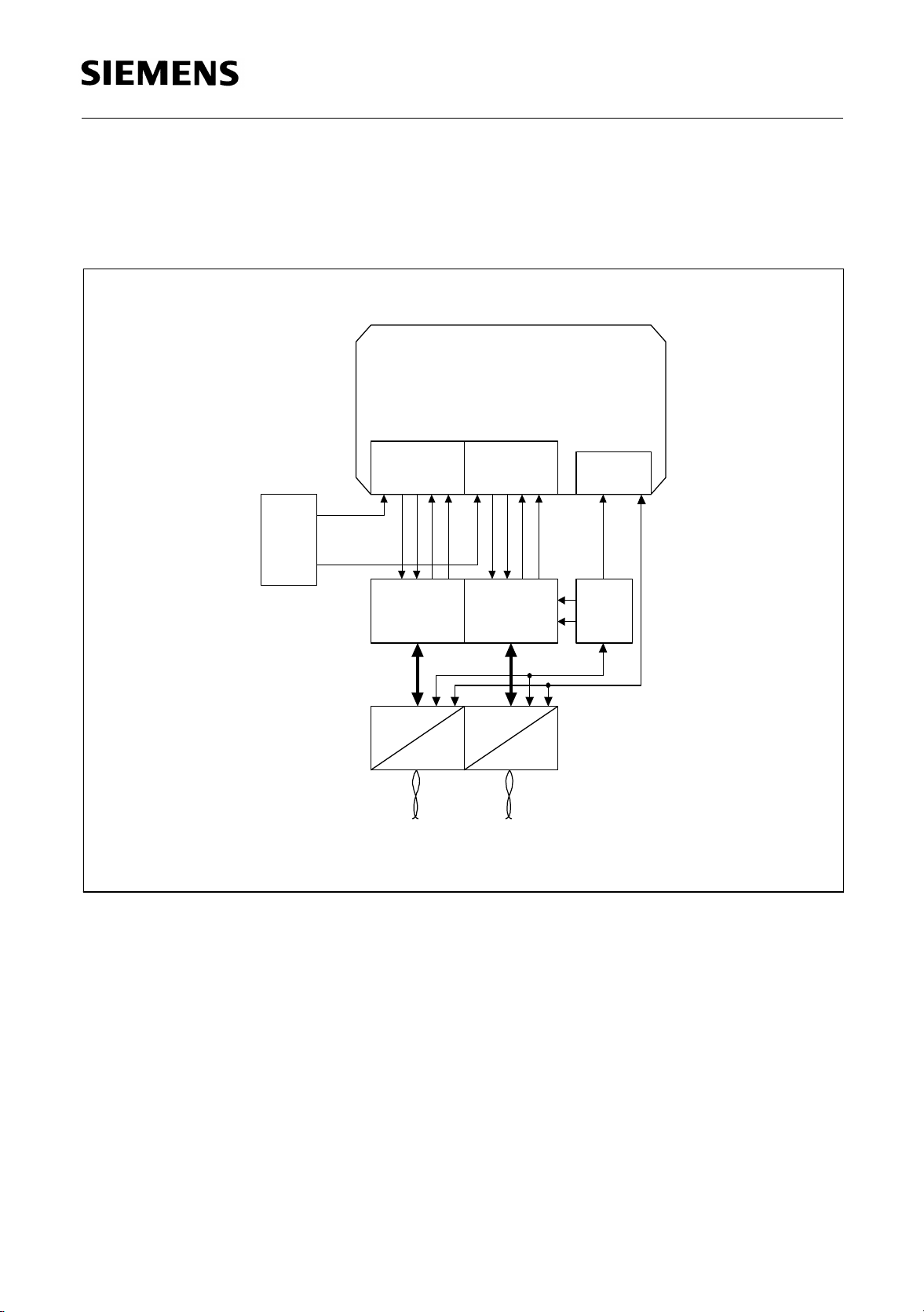
1.4 Typical Applications
The DSCC4 is designe d to handle up to 4 serial data ports in vario us configurations,
depending on the application. It transfers the data between the serial ports and a shared
memory via its 32 bit/33 MHz PCI Bus Interface which can optionally be configured as a
generic 32 bit de-multiplexed bus interface in the case that no PCI bus is applicable.
Figure 2 provides a gen eral overview upon system integ ration of the DS CC4 in a PCI
bus environment:
.
Local Peripheral Bus
.
.
. . .
PCI Bus
. . .
PEB 20534
DSCC4
. . .
Framer
Transceiver,
. . .
REQ
GNT
PCI
Bridge
PCI
Arbiter
Host Bus
...
Host Bus
Arbiter
CPU
Figure 2 General System Integration (PCI Bus Interface)
RAM
Bank
Semiconductor Group 24 Data Sheet 09.98
PEB 20534
Overview
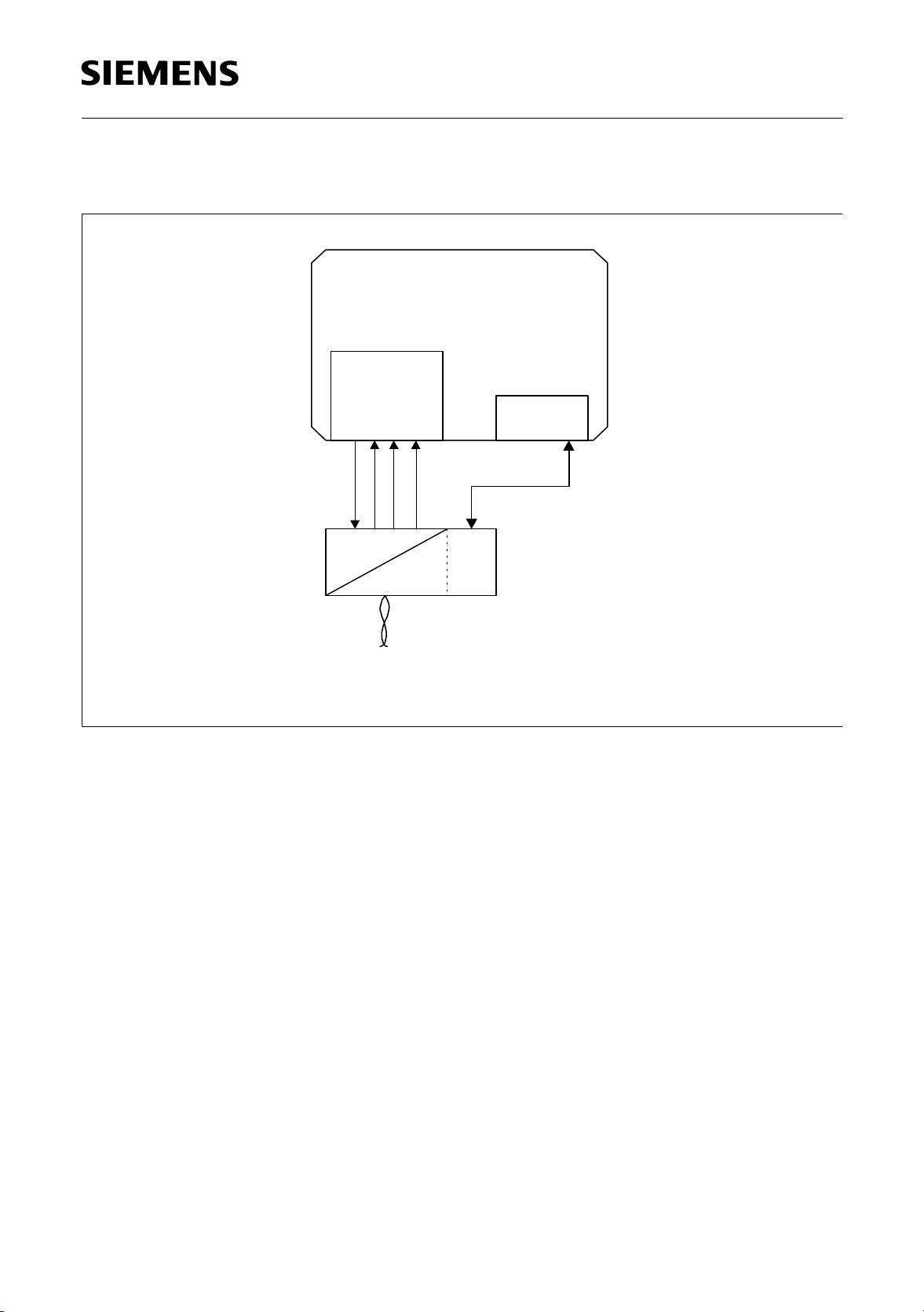
Connection of DSCC4 to PCI Bus according to PCI Specification Rev. 2.1 is free of any
glue-logic.
Figure 3 provides an overview upo n system integration in a non PC I bus environment
by the example of a Motorola 68360 CPU bus:
PEB 20534
Transceiver,
Framer
IDESL
TRDY
IRDY
DSCC4
FRAME
STOP
DEVSEL
W/R
A[31..2]
AD[31..0]
A1
A0
DEMUX
PAR
REQ
GNT
AS
Chip
Select
Decoder
Glue Logic
DS
DSACK
R/W
RAM
Bank
A[31..2]
D[31..0]
V
DD3
V
SS
Bus
Arbiter
BREQ
BGNT
BACK
MOTOROLA
68360
Figure 3 General System Integration (De-multiplexed Interface)
The glue-logic depends on the host bus which the DSCC4 should be connected to. The
example in Figure 3 shows the glue-lo gic for c onnec tion to an Motorol a 68360 like de-
multiplexed 32 bit bus.
See APPENDIX_xx for more detailed example.
Semiconductor Group 25 Data Sheet 09.98
PEB 20534
1.4.1 Ap plication Examples
1.4.1.1 HSSI Application
TxCLK0
Clock
Unit
TxCLK1
SCC0
TxD0
Overview
PEB 20534
DSCC4
SCC1
TxD1
TxCLKO1
RxD1
TxCLKO0
RxD0
RxCLK0
RxCLK1
GPP
GPi (input)
Loop Back
MUX
TTL
ECL
Loop Back
TTL
Line0
Figure 4 HSSI Application - DCE Adapter
MUX
Line1
Loop
Back
Control
Loop Ctrl.
ECL
Semiconductor Group 26 Data Sheet 09.98
PEB 20534
1.4.1.2 HSSI Application
TxD
TTL
SCCi
TxCLK
RxD
Overview
DSCC4
GPP
Loop Ctrl.
RxCLK
ECL
Line
Figure 5 HSSI Application - DTE Adapter
Semiconductor Group 27 Data Sheet 09.98
PEB 20534
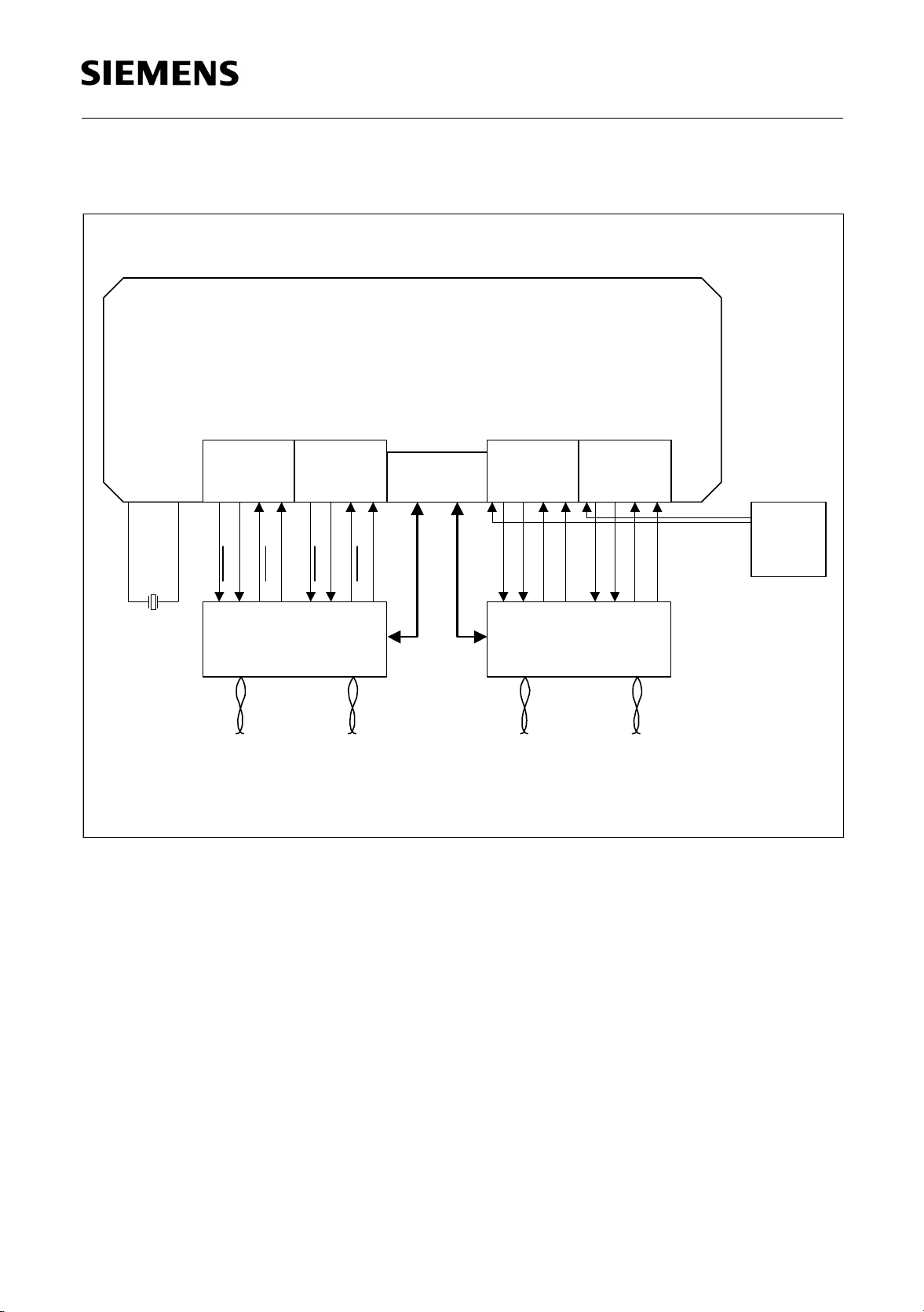
1.4.1.3 General Data Application
PEB 20534
DSCC4
SCC0
XTAL2
XTAL1
TxD0
RTS0
RxD0
CTS0
TxD1
SCC1
RTS1
RxD1
GPP
CTS1
SCC2 SCC3
RxD2
TxD2
RxCLK2
TxCLKO2
TxD3
TxCLKO3
RxD3
TxCLK2,
TxCLK3
RxCLK3
Overview
Clock
Unit
Line Transceiver
(RS232, RS485, ...)
ASYNC
Line0
Line1
Control (Loop, ...)
Figure 6 General Data Application
Control (Loop, ...)
Line Transceiver
SYNC/HDLC
Line2
Line3
Semiconductor Group 28 Data Sheet 09.98
PEB 20534
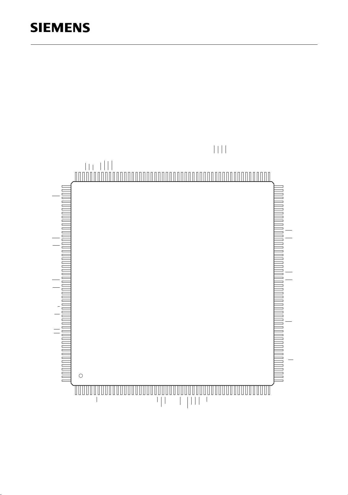
2 Pin Descriptions
2.1 Pin Diagra m
(top view)
SS
DD3
LHOLD
RESERVED1
LCSO
LBREQ
LHLDA
LD0/A16
LD1/A17
LD2/A18
V
LD3/A19
V
7 1013161922252831343740
NC20
V
DD3
V
SS
LRDY
LINTI1
RESERVED2
LCLK
LALE
V
DD3
V
SS
RxCLK2
TxCLK2
RxD2
TxD2
CTS2/CxD2/TCG2
CD2/FSC2/RCG2
RTS2
V
DD3
V
SS
XTAL1
XTAL2
RxCLK3
TxCLK3
RxD3
TxD3
CTS3/CxD3/TCG3
CD3/FSC3/RCG3
RTS3
V
DD3
V
SS
NC21
DEMUX
W/R
NC22
RST
V
DD3
CLK
V
SS
GNT
REQ
AD31
V
DD3
AD30
V
SS
AD29
AD28
V
DD3
V
SS
AD27
NC23
NC24
NC25
NC19
NC18
NC17
LBHE
LWR
LRD
156 153 108 105
157
160
163
166
169
172
175
178
181
184
187
190
193
196
199
202
205
208
41
LD4/A20
LD5/A21
LD6/A22
SS
LD7/A23
LD8/A24
V
DD3
SSVDD5VSSVDD3
V
V
DSCC4
PEB 20534
LD9/A25
LD10/A26
LD11/A27
LD12/A28
LD13/A29
LD14/A30
LD15/A31
SSVDD3
LA0/A0/GP2/MCS0
LA1/A1/GP1/MCS1
LA2/A2/GP2/MCS2
LA3/A3/GP3/MCS3
V
Pin Descriptions
SS
LA4/A4/GP4/MRST
DD3
LA5/A5/GP5/MTSR
LA6/A6/GP6/MSCLK
LA7/A7/GP7/Mx
LA8/A8/GP8
LA9/A9/GP9
V
V
111114117120123126129132135138141144147150
49 52
4643
NC15
NC14
NC13
104
101
98
95
92
89
86
83
80
77
74
71
68
65
62
59
56
53
NC12
V
SS
V
DD3
LA10/A10/GP10
LA11/A11/GP11
LA12/A12/GP12
LA13/A13/GP13
LA14/A14/GP14
LA15/A15/GP15
NC11
V
SS
V
DD3
RTS1
CD1/FSC1/RCG1
CTS1/CxD1/TCG1
TxD1
RxD1
TxCLK1
RxCLK1
NC10
TEST1
V
SS
V
DD3
RTS0
CD0/FSC0/RCG0
CTS0/CxD0/TCG0
TxD0
RxD0
TxCLK0
RxCLK0
TDO
TMS
TDI
TCK
V
SS
V
DD3
INTA
V
SS
AD0
V
DD3
AD1
AD2
AD3
AD4
AD5
AD6
C/BE0
V
SS
V
DD3
NC9
NC8
NC7
NC1
NC2
AD25
AD26
AD24
NC3/TRST
DD3
V
C/BE3
SS
V
IDSEL
AD23
AD21
AD22
SS
DD3
V
V
AD19
AD20
AD18
AD17
DD3
V
AD16
SS
V
C/BE2
FRAME
V
IRDY
DD5
SS
SS
DD3
V
V
V
TRDY
STOP
PERR
DEVSEL
PAR
SERR
C/BE1
AD15
AD14
V
AD13
DD3
V
SS
V
AD12
DD3
SS
V
AD11
AD9
AD10
AD8
AD7
NC4
NC5
NC6
ITP10573
Figure 7 Pin Configuration
Semiconductor Group 29 Data Sheet 09.98

PEB 20534
Pin Descriptions
2.2 Pin Definitions and Functions
Signal Type Definitions:
The following signal type definitions are mainly taken from the PCI Specification
Revision 2.1:
I
O
t/s, I/O
s/t/s
o/d
Signal Name Conventions:
Input is a standard input-only signal.
Totem Pole Output is a standard active driver.
Tri-State or I/O is a bi-directional, tri-state input/output pin.
Sustained Tri-State is an active low tri-state signal owned and driven
by one and only one agent at a time. (For further information refer to
the PCI Specification Revision 2.1)
Open Drain allows multiple devices to share as a wire-OR. A pull-up
is required to sustain the inactive state until another agent drives it,
and must be provided by the central resource.
NC
Reserved
Not Connected Pin
These pins are not bonded with the silicon. Although any potenti al at
these pins will not i mpact the device it is recommende d to leave them
unconnected. NC p ins mi ght be use d for addit ional f unctionalit y in l ater
versions of the device. Leaving them unconnected will guarentee
hardware compatibility to later device versions.
Reserved pins are for vendor specific use only and should be connected
as recommended to guarantee normal operation.
Semiconductor Group 30 Data Sheet 09.98
 Loading...