


ICs for Communications
ISDN DC Converter Circuit
IDCC
PEB 2023 Version 1.1
PEF 2023 Version 1.1
Data Sheet 08.97
DS 2
PEB 2023
PEF 2023
Revision History: Original Version: Data Sheet 08.97
Previous Releases: Data Sheet 02.97
Page Subjects (changes since last revision)
all Pages Additional to the normal temperatur e range devices PEB 2023 also the extended
temperature range devices PEF 2023 are specified in this Data Sheet.
21 The ambient temperature under bias is separately defined for PEB 2023 and PEF
2023.
22 The maximum limit values for line regulation
V
REF Line
and load regulation V
REF Load
are reduced. The typical values are adapted.
f
22 The maximum limit value for voltage stability of
is reduced. The typical value is
OSC
adapted.
T
22 The test condition ambient temperature range
V
stability of
REF
and f
23 The sense voltage
V
.
OSC
of the current limit comperator is separately defined for
Sense
is extended for temperature
A
PEB 2023 and PEF 2023.
Edition 08.97
This edition was realized using the software system FrameMaker.
Published by Siemens AG,
HL TS,
Balanstraße 73,
81541 Münc hen
©
Siemens AG 08.1997.
All Rights Reserved.
Attention pleas e !
As far as patents or other rights of third parties are concerned, liability is only assumed for components, not for applications, processes
and circui ts imp lem en te d with in co mpo ne nt s or ass emb li es.
The information describes the type of component and shall not be considered as assured characteristics.
Terms of delivery and rights to change design reserved.
For q uest io ns on tec hnolo gy , del i very an d pr ices pl ease c onta ct the Sem ico ndu ct or Gro up Offi ces i n Ger many o r th e Siem ens C ompa nies
and Representat iv es worldwide (se e address list ).
Due to technical requirements components may contain dangerous substances. For information on the types in question please contact
your nearest Siemens Office, Semiconductor Group.
Siemens AG is an approved CECC manufacturer.
Packing
Pl ea se use t he r ecycl in g opera to r s k n ow n t o you. We ca n a lso he lp you – get in touc h with yo u r nea r es t sales o f f ice. B y ag reem ent we will
take packing material back, if it is sorted. You must bear the costs of transport.
For packing material that is returned to us unsorted or which we are not obliged to accept, we shall have to invoice you for any costs incurred.
Compone nts use d in life-s upp ort de vi ces or sy stem s mu st be expres sl y authori z ed for such purpo se !
Critical components1 of the Semiconductor Group of Siemens AG, may only be used in life-support devices or systems2 with the express
written approval of the Semiconductor Group of Siemens AG.
1 A critical component is a component used in a life-support device or system whose failure can reasonably be expected to cause the
failure of that life-support device or system, or to affect its safety or effectiveness of that device or system.
2 Life support devices or systems are intended (a) to be implanted in the human body, or (b) to support and/or maintain and sustain hu -
man life. If they fail, it is reasonable to assume that the health of the user may be endangered.

PEB 2023
PEF 2023
Table of Contents Page
1 Overview. . . . . . . . . . . . . . . . . . . . . . . . . . . . . . . . . . . . . . . . . . . . . . . . . . . . . . . . 4
1.1 Features. . . . . . . . . . . . . . . . . . . . . . . . . . . . . . . . . . . . . . . . . . . . . . . . . . . . . . . . . 5
1.2 Pin Configuration . . . . . . . . . . . . . . . . . . . . . . . . . . . . . . . . . . . . . . . . . . . . . . . . . .6
1.3 Pin Definitions and Functio ns . . . . . . . . . . . . . . . . . . . . . . . . . . . . . . . . . . . . . . . .7
1.4 Functional Block Diagram . . . . . . . . . . . . . . . . . . . . . . . . . . . . . . . . . . . . . . . . . . . 8
1.5 System Integration . . . . . . . . . . . . . . . . . . . . . . . . . . . . . . . . . . . . . . . . . . . . . . . . 9
1.6 Surge Protection . . . . . . . . . . . . . . . . . . . . . . . . . . . . . . . . . . . . . . . . . . . . . . . . .14
1.7 Fast Input Undervoltage Detect ion. . . . . . . . . . . . . . . . . . . . . . . . . . . . . . . . . . . . 15
2 Functional De scription. . . . . . . . . . . . . . . . . . . . . . . . . . . . . . . . . . . . . . . . . . . .16
3 Electrica l Characteri st ics . . . . . . . . . . . . . . . . . . . . . . . . . . . . . . . . . . . . . . . . . 20
3.1 Absolute Maximum Ratin gs . . . . . . . . . . . . . . . . . . . . . . . . . . . . . . . . . . . . . . . . .20
3.2 Operating Range . . . . . . . . . . . . . . . . . . . . . . . . . . . . . . . . . . . . . . . . . . . . . . . . . 21
3.3 Static Thermal Resis tanc e . . . . . . . . . . . . . . . . . . . . . . . . . . . . . . . . . . . . . . . . . .21
3.4 DC Characteristics . . . . . . . . . . . . . . . . . . . . . . . . . . . . . . . . . . . . . . . . . . . . . . . .22
4 Package Outlines. . . . . . . . . . . . . . . . . . . . . . . . . . . . . . . . . . . . . . . . . . . . . . . . 25
Semiconductor Group 3 08.97

PEB 2023
PEF 2023
Overview
1 Overview
The PEB/F 2023 is a pulse width modulator circuit designed for fixed-frequency
switching regulators with ver y low power consum ption.
In telephone and ISDN-systems a high conversion yield is crucial to maintain
functionality in all supply conditions via S- or U-inter fa ces. The PEB/ F 2023 design and
technology realizes high conver sion efficiency and low power dissipation. The PEB/F
2023 is fully comp atible with the ITU-power recommenda tions of the S-interface. For
these reasons the PEB/F 2023 is especially suited for telephone and ISDNenvironments.
Coupled with a few external components it can provide a stable 5V DC-supply for
subscriber terminals (TE’s) or network terminators (NT’s). It can additionally be
programmed f or higher out put voltages , e.g. to supply the S-lines.
It should be recognized that the PEB/F 2023 can also be used in num erous DC/DCconversion syste ms other than ISDN-power supplies. For examp le, in a special supply
voltage range the PEB/F 2023 can be supplied from a 12V battery.
For detailed technical information abou t "Process ing Guidel i nes" and
"Quality Assurance" for ICs, see our "Product Overview".
Semiconductor Group 4 08.97
ISDN DC Converter Circuit
IDCC
PEB 2023
PEF 2023
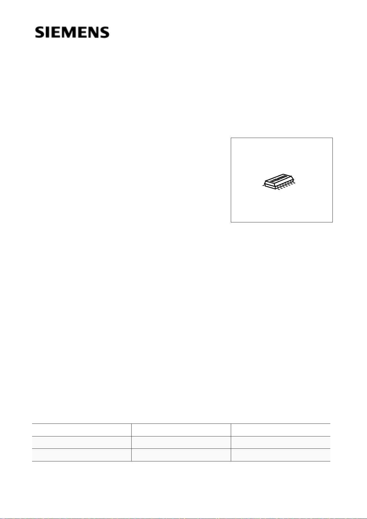
Data Sheet SPT 75 R
P-DSO-14
1.1 Features
• Switched Mode DC/DC Converter
• ITU ISDN Compatible
• Low Power Dissipation
• Supply Voltage Range 0: 8V to 16V
Supply Voltage Range 1: 12V to 80V
Supply Voltage Range 2: 22V to 90V
(pin striping selects between range 1 and range 2)
Supply Voltage Range 3, with shifting by an external zener diode: U
(minimum zener voltage U
= 14V)
ZD
• Programmable Overcurrent Protection
• Soft Start
• Power Housekeeping Input
• Input Undervoltag e Detect ion
• High Input Impedance (<10µA) During Undervoltage Condition
• Oscillator Synchronization Input/Ou tput
• High Voltage Smart Power Technology 75V
• P-DSO-14/1 Package
Type Ordering Code Package
+8V to UZD+90V
ZD
PEB 2023 Q67100-H6830 P-DSO-14
PEF 2023 Q67220-H1059 P-DSO-14
Semiconductor Group 5 08.97
1.2 Pin Configuration
(top view)
PEB 2023
PEF 2023
Overview
P-DSO-14
V
REF
GND
GA
V
EXT
C
SS
V
1
I
P
2
3
IDCC
4
PEB 2023
PEF 2023
5
6
S
7
14
13
12
11
10
RC
SYNC
UVx
UV
V
N
9
8
V
P
COMP
Semiconductor Group 6 08.97
1.3 Pin Definition s and Functions
PEB 2023
PEF 2023
Overview
Pin No. Symbol Input (I)
Function
Output (O)
1 V
2
REF
I
P
3 GND I All analog and digital signals are referred to this pin.
4 GA O Output of the FET-driver.
5
6
7
V
C
V
EXT
SS
S
O Output of the 4V reference voltage.
I
When the voltage difference between
I
and GND
P
exceeds 100mV, the digital cur rent limiting
becomes active and turns off the external FET for
the rest of this oscillator period.
I/O Output of the internal supply. Via V
the internal
EXT
low-voltage-circuits can be supplied from an
external DC-supply in order to reduce chip power
dissipation. In supply voltage range 0 the positive
supply voltage must be connected via a resistor to
this pin.
I The capacitor at this pin determines the soft-start
characteristic.
I VS is the positive input voltage for supply volt age
range 1, 2 and 3. Must be connected to GND via a
resistor when using supply voltage range 0.
8 COMP O Error amplifier output and Pulse Width Modulator
(PWM) input for loop stabili zation network.
9
10
V
P
V
N
I Non-inverting input of the error amplifier.
I Inverting input of the error amplifier.
11 UV I Input undervoltage lockout. The input undervoltage
lockout level depends on the used supply voltage
V
range. Must be connected to pin
when using
S
supply voltage range 0.
12 UVx I If this pin is connected to UV, then supply range 1 is
selected. If this pin is not connected (floating), then
supply range 2 or supply range 3 can be used. Must
V
be connected to pin
when using supply voltage
EXT
range 0.
13 SYNC I/O Input for synchronization of the oscillator to an
external frequency, or output to synchronize
multiple devices .
14 RC I The external timing components of the ramp
generator are attached to this pin.
Semiconductor Group 7 08.97
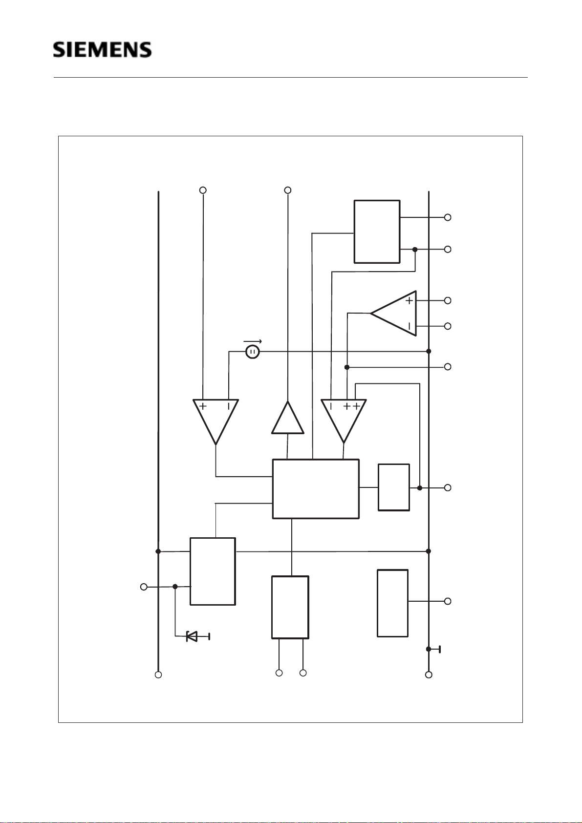
1.4 Functional Block Diagram
PEB 2023
PEF 2023
Overview
IP
100 mV
CURRENT LIMITING
GA
OUTPUT DRIVER
SAWTOOTH
OSCILLATOR
AMPL.
ERROR
PWM
SYNC
RC
P
V
N
V
COMP
Figure 1
Block Diagram
EXT
V
V
SS
LOGIC
CONTROL
BIASING
SUPPLY AND
UNDER-
VOLTAGE
DETECTION
S
9.4 V
UV
UVx
SOFT
START
VOLTAGE
REFERENCE
C
V
GND
REF
Semiconductor Group 8 08.97
 Loading...