

Siemens HYB511000BJ-50, HYB511000BJ-60, HYB511000BJ-70, HYB511000BJL-50, HYB511000BJL-60 Datasheet
...
Semiconductor Group 33 01.95
• 1 048 576 words by 1-bit organization
• Fast access and cycle time
50 ns access time
95 ns cycle time (-50 version)
60 ns access time
130 ns cycle time (-60 version)
70 ns access time
130 ns cycle time (-70 version)
• Fast page mode cycle time
35 ns (-50 version)
40 ns (-60 version)
45 ns (-70 version)
• Low power dissipation
max. 495 mW active (-50 version)
max. 440 mW active (-60 version)
max. 385 mW active (-70 version)
max. 5.5 mW standby
max. 1.1 mW standby for L-version
Ordering Information
Type Ordering Code Package Description
HYB 511000BJ-50 Q67100-Q1056 P-SOJ-26/20-1 DRAM (access time 50 ns)
HYB 511000BJ-60 Q67100-Q518 P-SOJ-26/20-1 DRAM (access time 60 ns)
HYB 511000BJ-70 Q67100-Q519 P-SOJ-26/20-1 DRAM (access time 70 ns)
HYB 511000BJL-50 on request P-SOJ-26/20-1 DRAM (access time 50 ns)
HYB 511000BJL-60 Q67100-Q526 P-SOJ-26/20-1 DRAM (access time 60 ns)
HYB 511000BJL-70 Q67100-Q527 P-SOJ-26/20-1 DRAM (access time 70 ns)
1 M × 1-Bit Dynamic RAM
Low Power 1 M × 1-Bit Dynamic RAM
Advanced Information
HYB 511000BJ-50/-60/-70
HYB 511000BJL-50/-60/-70
• Single + 5 V (± 10 %) supply with a built-in
V
BB
generator
• Output unlatched at cycle end allows two-
dimensional chip selection
• Common I/O capability using “early write”
operation
• Read-modify-write, CAS-before-RAS
refresh,
RAS-only refresh, hidden-refresh,
fast page mode capability and test mode
capability
• All inputs, outputs and clocks
TTL-compatible
• 512 refresh cycles/8 ms
512 refresh cycles/64 ms
for L-version only
• Plastic Packages: P-SOJ-26/20-1
Semiconductor Group 34
HYB 511000BJ/BJL-50/-60/-70
1 M × 1-DRAM
The HYB 511000BJ/BJL is the new generation dynamic RAM organized as 1 048 576 words by
1-bit. The HYB 511000BJ/BJL utilizes CMOS silicon gate process technology as well as advanced
circuit techniques to provide wide operating margins, both internally and for the system user.
Multiplexed address inputs permit the HYB 511000BJ/BJL to be packaged in a standard plastic
P-SOJ-26/20. This package size provides high system bit densities and is compatible with
commonly used automatic testing and insertion equipment. System oriented features include single
+ 5 V (± 10 %) power supply, direct interfacing with high-performance logic device families such as
Schottky TTL. “Test Mode” function is implemented. The HYB 511000BJL are specially selected for
low power battery backup applications.
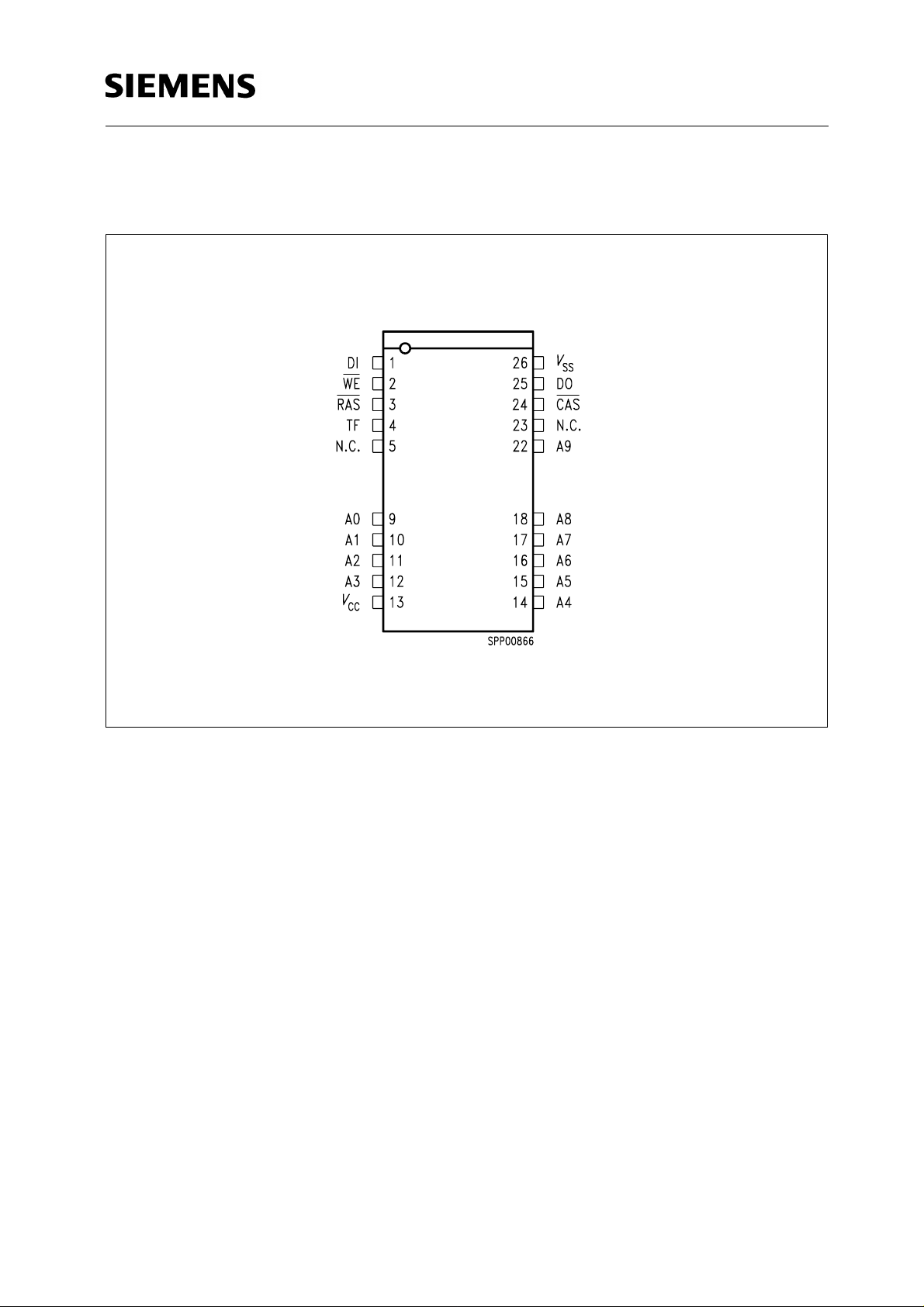
Pin Definitions and Functions
Pin No. Function
A0-A9 Address Inputs
RAS Row Address Strobe
DI Data In
DO Data Out
CAS Column Address Strobe
WE Read/Write Input
V
CC
Power Supply (+ 5 V)
V
SS
Ground (0 V)
TF Test Function
N.C. No Connection
Semiconductor Group 35
HYB 511000BJ/BJL-50/-60/-70
1 M × 1-DRAM
Pin Configuration
(top view)
SOJ-26/20-1
Semiconductor Group 36
HYB 511000BJ/BJL-50/-60/-70
1 M × 1-DRAM
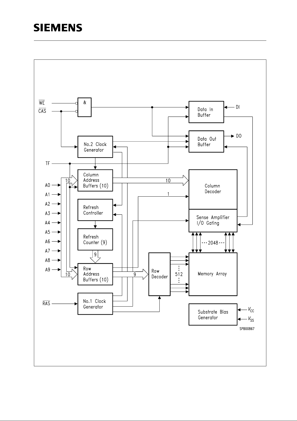
Block Diagram
Semiconductor Group 37
HYB 511000BJ/BJL-50/-60/-70
1 M × 1-DRAM
Absolute Maximum Ratings
Operating temperature range .........................................................................................0 to + 70 ˚C
Storage temperature range......................................................................................– 55 to + 150 ˚C
Soldering temperature ............................................................................................................260 ˚C
Soldering time.............................................................................................................................10 s
Input/output voltage ........................................................................................................– 1 to + 7 V
Test Function Input voltage ....................................................................................... – 1 to + 10.5 V
Power supply voltage......................................................................................................– 1 to + 7 V
Power dissipation..................................................................................................................... 0.6 W
Data out current (short circuit) ................................................................................................50 mA
Note:Stresses above those listed under “Absolute Maximum Ratings” may cause permanent
damage of the device. Exposure to absolute maximum rating conditions for extended periods
may affect device reliability.
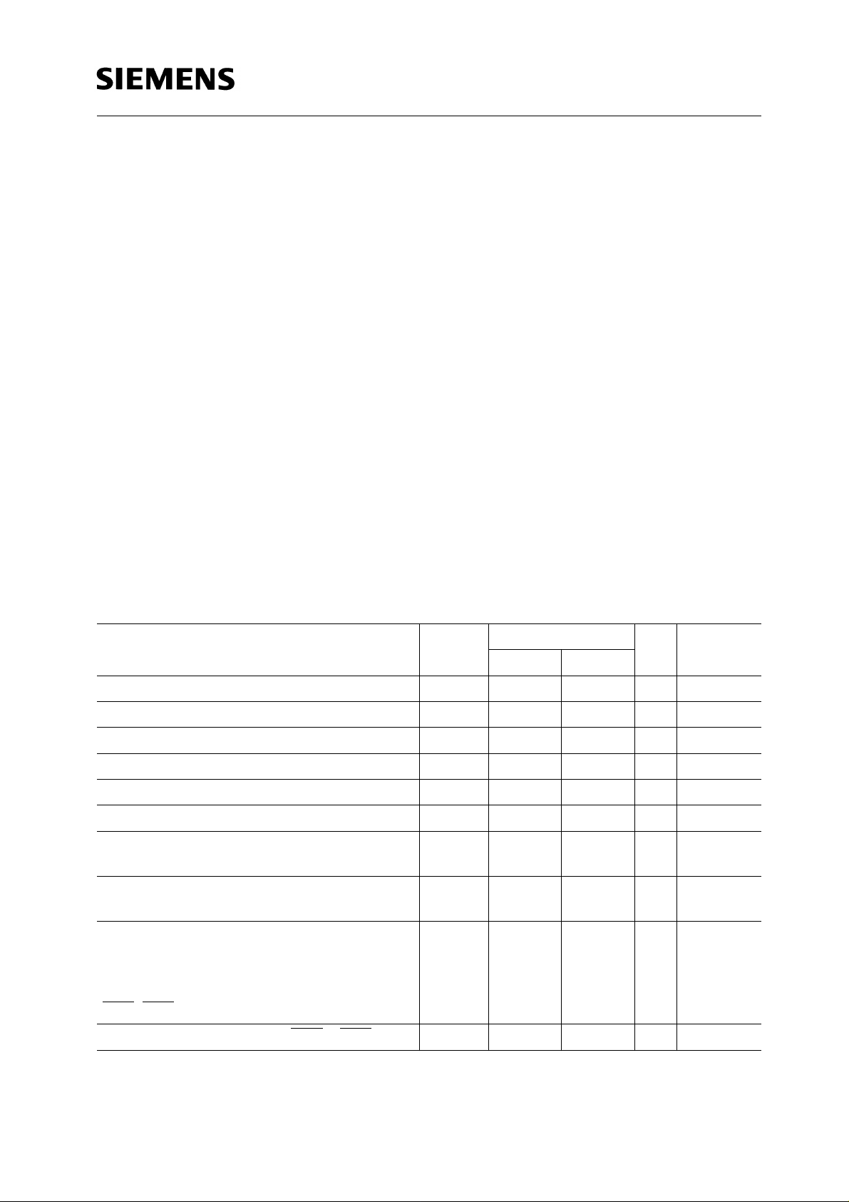
DC Characteristics
T
A
= 0 to 70 ˚C; VSS = 0 V; VCC = 5 V ± 10 %
Parameter Symbol Limit Values Unit Test
Condition
min. max.
Input high voltage
V
IH
2.4 6.5 V
1)
Input low voltage V
IL
– 1.0 0.8 V
1)
Test enable input high voltage V
IH(TF)
V
CC
+ 4.5 10.5 V
1)
Test disable input low voltage V
IL(TF)
– 1.0 VCC + 1.0 V
1)
Output high voltage (I
OUT
= – 5 mA) V
OH
2.4 – V
1)
Output low voltage (I
OUT
= 4.2 mA) V
OL
– 0.4 V
1)
Input leakage current, any input except TF
(0 V ≤
V
IN
≤ 6.5 V, all other pins = 0 V)
I
I(L)
– 10 10 µA
1)
Output leakage current
(DO is disabled, 0 V ≤
V
OUT
≤ 5.5 V)
I
O(L)
– 10 10 µA
1)
Average VCC supply current:
-50 version
-60 version
-70 version
(RAS, CAS, address cycling: tRC = tRC min.)
I
CC1
–
–
–
90
80
70
mA
mA
mA
2) 3)
2) 3)
2) 3)
Standby VCC supply current (RAS = CAS = VIH) I
CC2
–2mA–
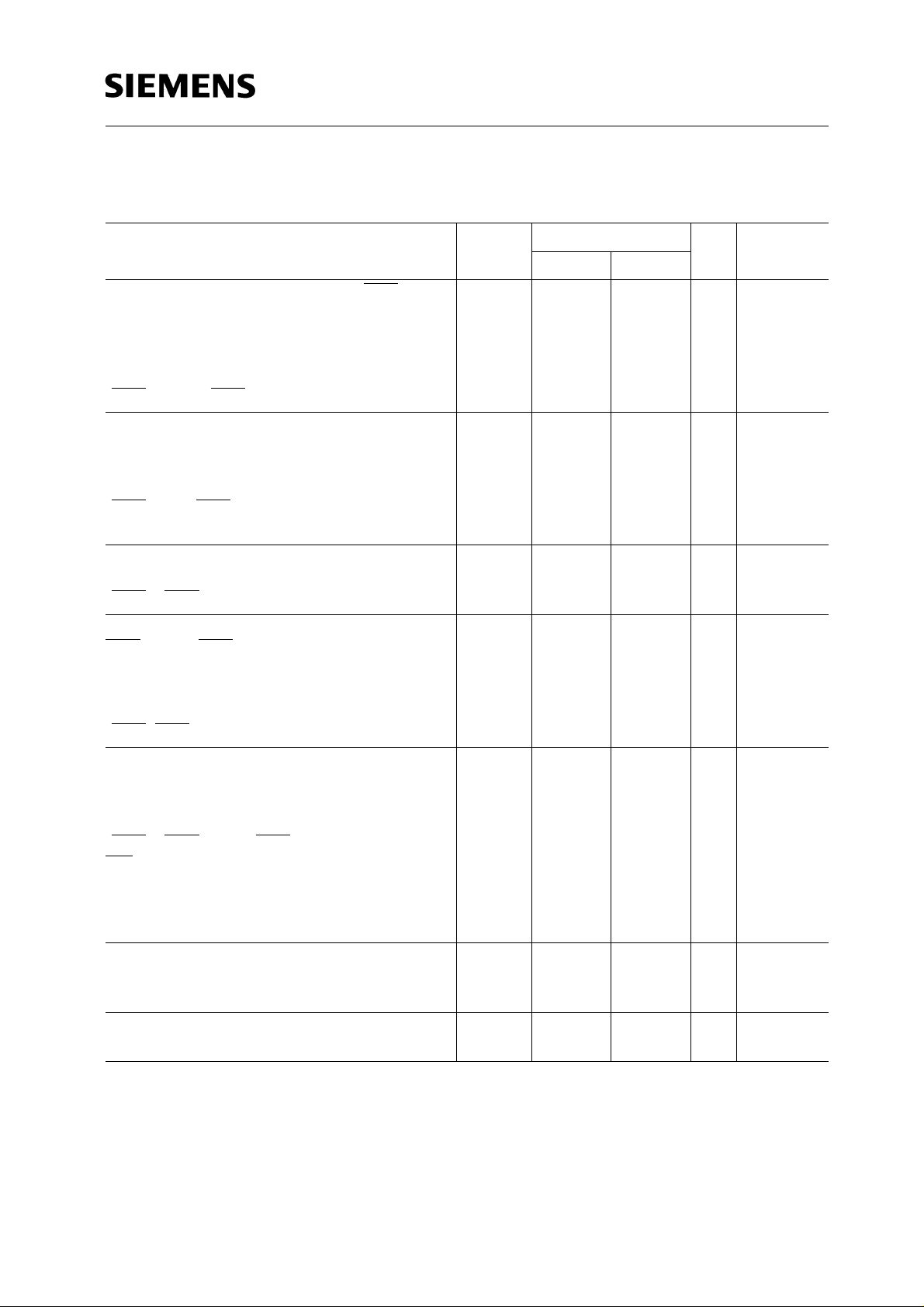
Semiconductor Group 38
HYB 511000BJ/BJL-50/-60/-70
1 M × 1-DRAM
Average VCC supply current during RAS only
refresh cycles: -50 version
-60 version
-70 version
(
RAS cycling: CAS = VIH: tRC = tRC min.)
I
CC3
–
–
–
90
80
70
mA
mA
mA
2)
2)
2)
Average VCC supply current during fast page
modes: -50 version
-60 version
-70 version
(
RAS = VIL, CAS, address cycling:
t
PC
= tPC min.)
I
CC4
–
–
–
70
60
50
mA
mA
mA
2) 3)
2) 3)
2) 3)
Standby VCC supply current
L-Version
(
RAS = CAS = VCC – 0.2 V)
I
CC5
–
–
1
200
mA
µA
1)
1)
Average VCC supply current during
CAS-before-RAS refresh mode:
-50 version
-60 version
-70 version
(RAS, CAS, address cycling: tRC = tRC min.)
I
CC6
–
–
–
90
80
70
mA
mA
mA
2)
2)
2)
For L-version only:
Battery backup current:
average power supply current, battery backup
mode:
(
CAS = CAS before RAS cycling or 0.2 V,
WE = VCC – 0.2 V or 0.2 V,
A0 to A9 =
V
CC
– 0.2 V or 0.2 V,
DI =
V
CC
– 0.2 V or 0.2 V open,
t
RC
= 125 µs, t
RAS
= t
RAS
min. ~ 1 µs)
I
CC7
– 300 µA
2)
Input leakage current (only TF)
(0 V ≤ VIN (TF) ≤ VCC + 0.5 V)
All other pins not under test = 0 V
I
ITF(L)
– 10 + 10 µA
1)
Test function input current
(
V
CC
+ 4.5 ≤ VIN (TF) ≤ 10.5 V)
I
TF
–1mA
1)
DC Characteristics (cont’d)
T
A
= 0 to 70 ˚C; VSS = 0 V; VCC = 5 V ± 10 %
Parameter Symbol Limit Values Unit Test
Condition
min. max.
Semiconductor Group 39
HYB 511000BJ/BJL-50/-60/-70
1 M × 1-DRAM
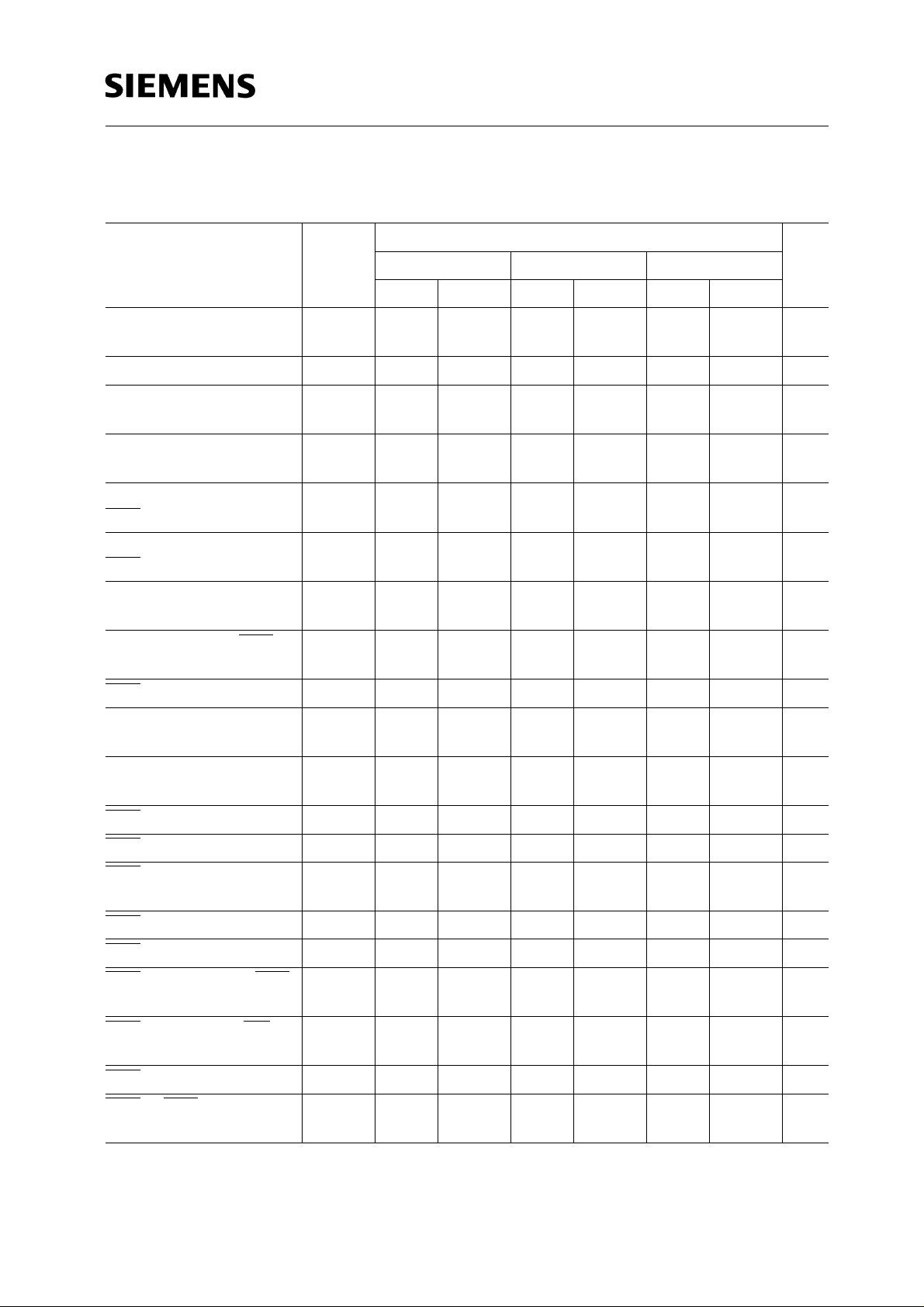
AC Characteristics
4) 13)
T
A
= 0 to 70 ˚C; VCC = 5 V ± 10 %; tT = 5 ns
Parameter Symbol Limit Values Unit
-50 -60 -70
min. max. min. max. min. max.
Random read or write
cycle time
t
RC
95 – 110 – 130 – ns
Read-write cycle time
t
RWC
115 – 130 – 155 – ns
Fast page mode cycle
time
t
PC
35 – 40 – 45 – ns
Fast page mode readwrite cycle time
t
PRWC
55 – 60 – 70 – ns
Access time from
RAS
6) 11)
t
RAC
–50–60–70ns
Access time from
CAS
6) 11)
t
CAC
–15–15–20ns
Access time from column
address
6) 12)
t
AA
–25–30–35ns
Access time from
CAS
precharge
6)
t
CPA
–30–35–40ns
CAS to output in low-Z
6)
t
CLZ
0– 0– 0– ns
Output buffer turn-off
delay
7)
t
OFF
015020020ns
Transition time
(rise and fall)
5)
t
T
350350350ns
RAS precharge time t
RP
35 – 40 – 50 – ns
RAS pulse width t
RAS
50 10.000 60 10.000 70 10.000 ns
RAS pulse width (fast
page mode)
t
RASP
50 100.000 60 100.000 70 100.000 ns
RAS hold time t
RSH
15 – 15 – 20 – ns
CAS hold time t
CSH
50 – 60 – 70 – ns
RAS hold time from CAS
precharge (FPM)
t
RHCP
30 – 35 – 45 – ns
CAS precharge to WE
delay time (FPM RMW)
t
CPWD
30 – 35 – 45 – ns
CAS pulse width t
CAS
15 10.000 15 10.000 20 10.000 ns
RAS to CAS delay
time
11)
t
RCD
20 35 20 45 20 50 ns
 Loading...