

Siemens HYB39S16800BT-8, HYB39S16400BT-10, HYB39S16400BT-8, HYB39S16800BT-10, HYB39S16160BT-10 Datasheet
...
HYB39S16400/800/160BT-8/-10
16MBit Synchronous DRAM
16 MBit Synchronous DRAM
Advanced Information
• High Performance:
-8 -10 Units
fCK(max.) 125 100 MHz
tCK3 8 10 ns
tAC3 6 7 ns
tCK2 10 13.3 ns
tAC2 6 8 ns
• Fully Synchronous to Positive Clock Edge
• 0 to 70 °C operating temperature
• Dual Banks controlled by A11 ( Bank Select)
• Programmable CAS Latency : 2, 3
• Programmable Wrap Sequence : Sequential
or Interleave
• Programmable Burst Length: 1, 2, 4, 8
• full page(optional) for sequencial wrap
around
• Multiple Burst Read with Single Write
Operation
• Automatic and Controlled Precharge
Command
• Data Mask for Read / Write control (x4, x8)
• Dual Data Mask for byte control ( x16)
• Auto Refresh (CBR) and Self Refresh
• Suspend Mode and Power Down Mode
• 4096 refresh cycles / 64 ms
• Random Column Address every CLK
( 1-N Rule)
• Single 3.3V +/- 0.3V Power Supply
• LVTTL Interface
• Plastic Packages:
P-TSOPI-44 400mil width ( x4, x8 )
P-TSOPII -50 400 mil width ( x 16 )
• -8 version for PC100 applications
The HYB39S16400/800/160BT are dual bank Synchronous DRAM’s based on the die revisions “D“,
& “E” and organized as 2 banks x 2MBit x4, 2 banks x 1MBit x8 and 2 banks x 512kbit x16
respectively. These synchronous devices achieve high speed data transfer rates up to 125 MHz by
employing a chip architecture that prefetches multiple bits and then synchronizes the output data to
a system clock. The chip is fabricated with SIEMENS’ advanced 16MBit DRAM process technology.
The device is designed to comply with all JEDEC standards set for synchronous DRAM products,
both electrically and mechanically. All of the control, address, data input and output circuits are
synchronized with the positive edge of an externally supplied clock.
Operating the two memory banks in an interleaved fashion allows random access operation to occur
at higher rate than is possible with standard DRAMs. A sequential and gapless data rate of up to 125
MHz is possible depending on burst length, CAS
latency and speed grade of the device.
Auto Refresh (CBR) and Self Refresh operation are supported. These devices operate with a single
3.3V +/- 0.3V power supply and are available in TSOPII packages.
These Synchronous DRAM devices are available with LV-TTL interfaces.
Semiconductor Group 1 4.98
HYB39S16400/800/160BT-8/-10
16MBit Synchronous DRAM
Ordering Information
Type Ordering Code Package Description
LVTTL-version:
HYB 39S16400BT-8 P-TSOPII-44 (400mil) 125MHz 2B x 2M x 4 SDRAM
HYB 39S16400BT-10 P-TSOPII-44-(400mil) 100MHz 2B x 2M x 4 SDRAM
HYB 39S16800BT-8 P-TSOPII-44-(400mil) 125MHz 2B x 1M x 8 SDRAM
HYB 39S16800BT-10 P-TSOPII-44 (400mil) 100MHz 2B x 1M x 8 SDRAM
HYB 39S16160BT-8 P-TSOPII-50 (400mil) 125MHz 2B x 512k x 16 SDRAM
HYB 39S16160BT-10 P-TSOPII-50-(400mil) 100MHz 2B x 512k x 16 SDRAM
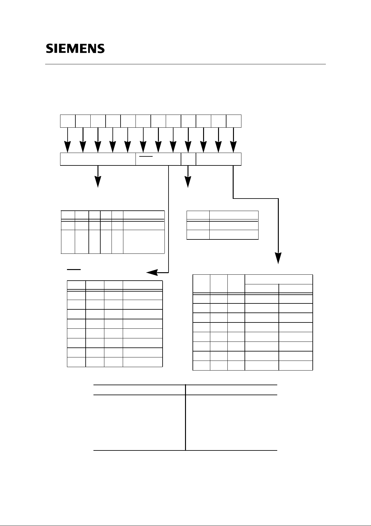
Pin Description and Pinouts:
CLK Clock Input DQ Data Input /Output
CKE Clock Enable DQM, LDQM, UDQM Data Mask
CS
RAS
CAS
WE
A0-A10 Address Inputs NC not connected
A11 (BS) Bank Select
Chip Select Vdd Power (+3.3V)
Row Address Strobe Vss Ground
Column Address Strobe Vddq Power for DQ’s (+ 3.3V)
Write Enable Vssq Ground for DQ’s
Semiconductor Group 2
HYB39S16400/800/160BT-8/-10
16MBit Synchronous DRAM
Vdd
NC
Vssq
DQ0
Vddq
NC
Vssq
DQ1
Vddq
NC
NC
WE
CAS
RAS
CS
A11
A10
A0
A1
A2
A3
Vdd
1
2
3
4
5
6
7
8
9
10
11
12
13
14
15
16
17
18
19
20
21
22
HYB39S16400BT HYB39S16800BT
2 Bank x 2MBit x 4
TSOPII-44
( 400 mil x 725 mil)
44
43
42
41
40
39
38
37
36
35
34
33
32
31
30
29
28
27
26
25
24
23
Vss
NC
Vssq
DQ3
Vddq
NC
Vssq
DQ2
Vddq
NC
NC
DQM
CLK
CKE
NC
A9
A8
A7
A6
A5
A4
Vss
Vdd
DQ0
DQ1
Vssq
DQ2
DQ3
Vddq
DQ4
DQ5
Vssq
DQ6
DQ7
Vddq
LDQM
WE
CAS
RAS
CS
A11
A10
A0
A1
A2
A3
Vdd
1
2
3
4
5
6
7
8
9
10
11
12
13
14
15
16
17
18
19
20
21
22
23
24
25
44
43
42
41
40
39
38
37
36
35
34
33
32
31
30
29
28
27
26
50
49
48
47
46
45
Vdd
DQ0
Vssq
DQ1
Vddq
DQ2
Vssq
DQ3
Vddq
NC
NC
WE
CAS
RAS
CS
A11
A10
A0
A1
A2
A3
Vdd
1
2
3
4
5
6
7
8
9
10
11
12
13
14
15
16
17
18
19
20
21
22
2 Bank x 1MBit x 8
TSOPII-44
( 400 mil x 725 mil )
Vss
DQ15
DQ14
Vssq
DQ13
DQ12
Vddq
DQ11
DQ10
Vssq
DQ9
DQ8
Vddq
NC
UDQM
CLK
CKE
NC
A9
A8
A7
A6
A5
A4
Vss
44
43
42
41
40
39
38
37
36
35
34
33
32
31
30
29
28
27
26
25
24
23
Vss
DQ7
Vssq
DQ6
Vddq
DQ5
Vssq
DQ4
Vddq
NC
NC
DQM
CLK
CKE
NC
A9
A8
A7
A6
A5
A4
Vss
HYB39S16160BT
2 Bank x 512kbit x 16
TSOPII-50
( 400 mil x 825 mil )
Semiconductor Group 3
HYB39S16400/800/160BT-8/-10
16MBit Synchronous DRAM
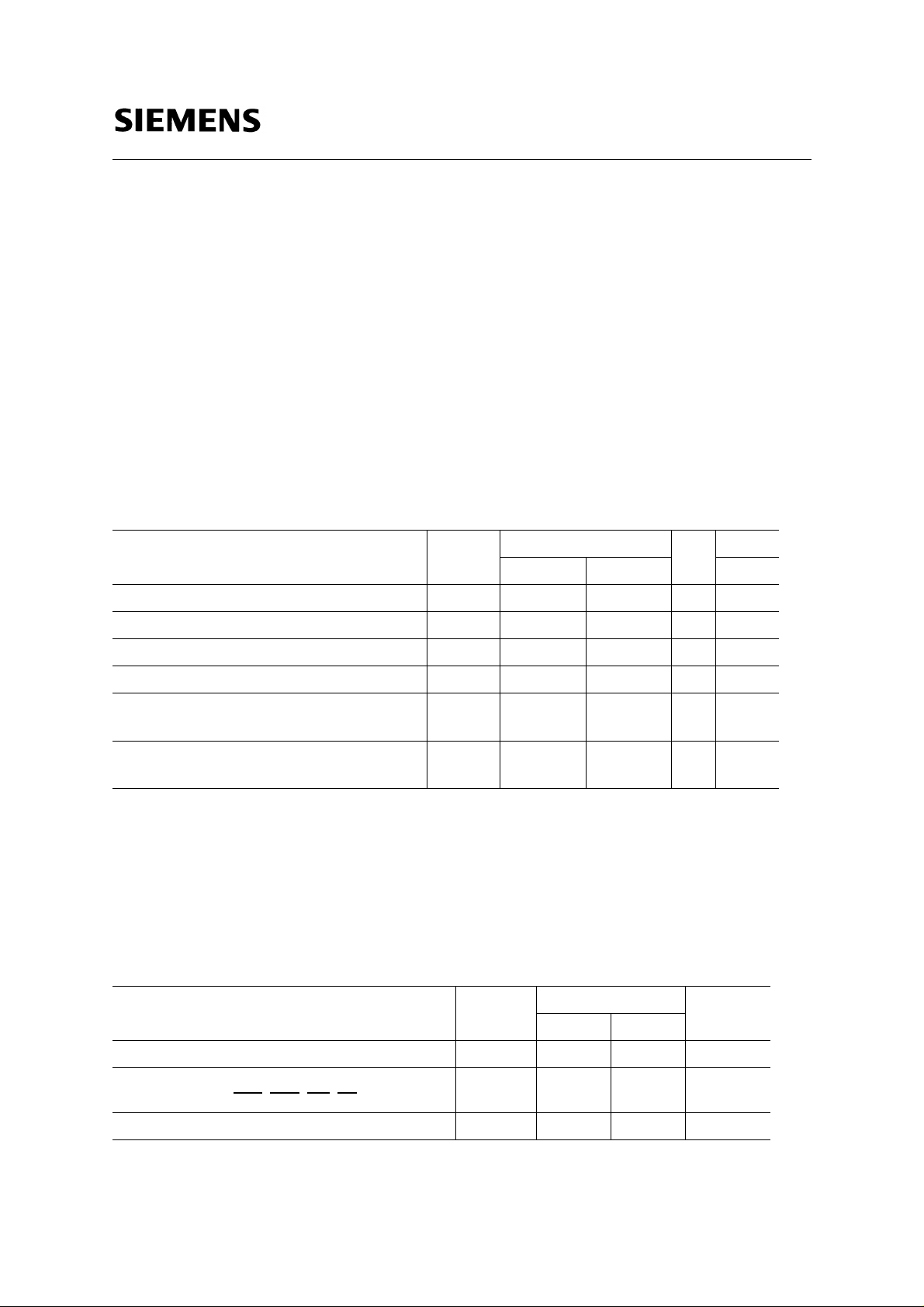
Signal Pin Description
Pin Type Signal Polarity Function
CLK Input Pulse
CKE Input Level
CS
RAS
CAS
A0 -
A10
Input Pulse
,
WEInput Pulse
Input Level
Positive
Edge
Active
High
Active
Low
Active
Low
—
The system clock input. All of the SDRAM inputs are sampled on the rising
edge of the clock.
Activates the CLK signal when high and deactivates the CLK signal when
low, thereby inititiates either the Power Down mode, Suspend mode or the
Self Refresh mode.
CS
enables the command decoder when low and disables the command
decoder when high. When the command decoder is disabled, new
commands are ignored but previous operations continue.
When sampled at the positive rising edge of the clock, CAS
define the command to be executed by the SDRAM.
During a Bank Activate command cycle, A0-A10 defines the row address
(RA0-RA10) when sampled at the rising clock edge.
During a Read or Write command cycle, A0-A9 defines the column
address (CA0-CAn) when sampled at the rising clock edge.CAn depends
from the SDRAM organisation.
4M x 4 SDRAM CAn = CA9
2M x 8 SDRAM CAn = CA8
1M x 16 SDRAM CAn = CA7
In addition to the column address, A10 is used to invoke autoprecharge
operation at the end of the burst read or write cycle. If A10 is high,
autoprecharge is selected and A11 defines the bank to be precharged
(low=bank A, high=bank B). If A10 is low, autoprecharge is disabled.
During a Precharge command cycle, A10 is used in conjunction with A11
to control which bank(s) to precharge. If A10 is high, both bank A and bank
B will be precharged regardless of the state of A11. If A10 is low, then A11
is used to define which bank to precharge.
, RAS, and WE
A11
(BS)
DQx
DQM
LDQM
UDQM
VDD,
VSS
VDDQ
VSSQ
Input Level
Input
Output
Input Pulse
Supply Power and ground for the input buffers and the core logic.
Supply — —
Level
Active
High
Selects which bank is to be active. A11 low selects bank A and A11 high
—
selects bank B.
Data Input/Output pins operate in the same manner as on conventional
—
DRAMs.
The Data Input/Output mask places the DQ buffers in a high impedance
state when sampled high. In Read mode, DQM has a latency of two clock
cycles and controls the output buffers like an output enable. In Write
mode, DQM has a latency of zero and operates as a word mask by
allowing input data to be written if it is low but blocks the write operation if
DQM is high.
Isolated power supply and ground for the output buffers to provide
improved noise immunity.
Semiconductor Group 4
HYB39S16400/800/160BT-8/-10
16MBit Synchronous DRAM
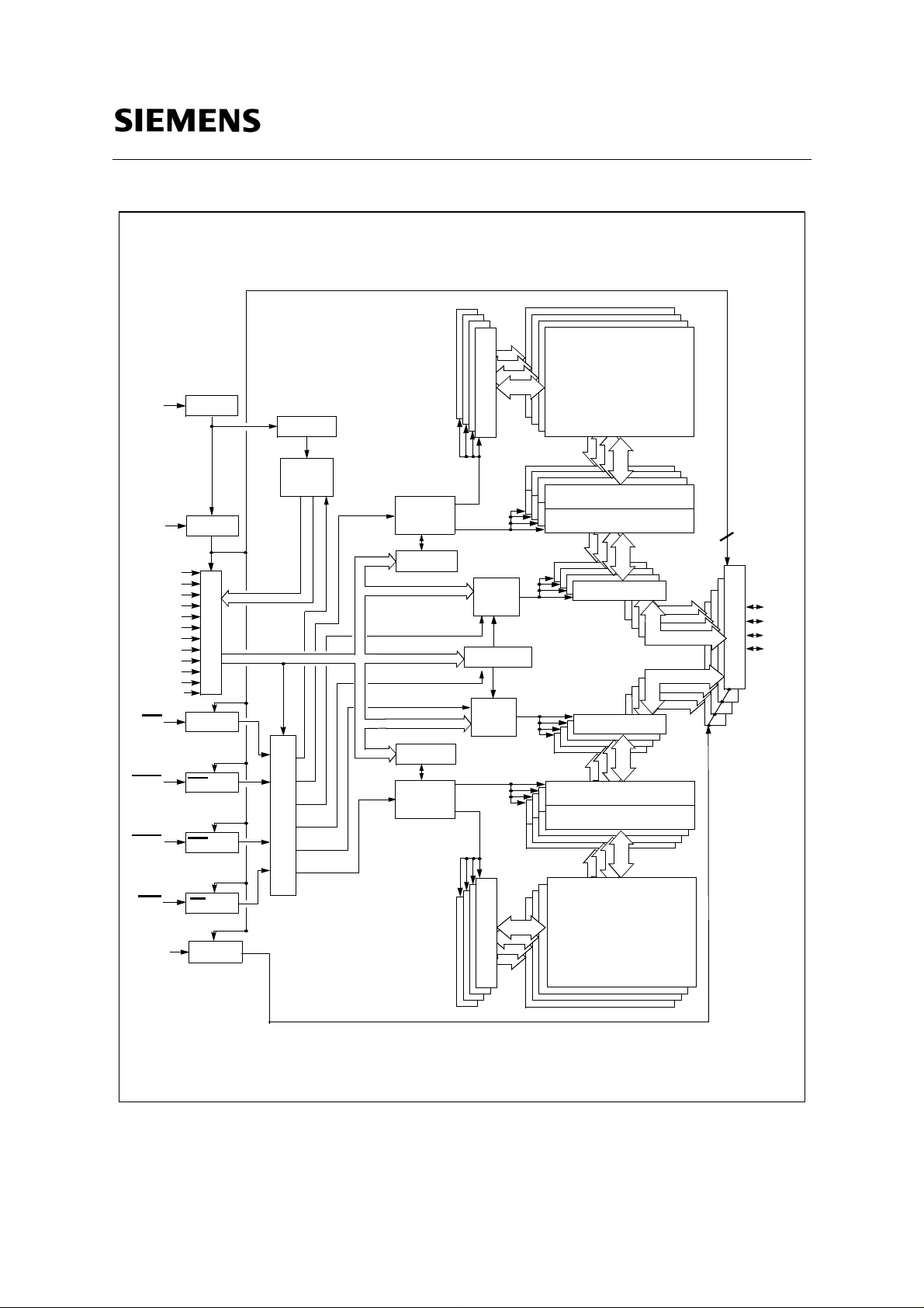
Row Decoder
CKE
CLK
A0
A1
A2
A3
A4
A5
A6
A7
A8
A9
A10
A11 (BS)
CS
RAS
CAS
CKE Buffer
CLK Buffer
Address Buffers (12)
CS Buffer
RAS Buffer
CAS Buffer
Refresh Clock
12
12
Command Dec oder
Self
Row
Address
Counter
11
11
Bank A
Row/Column
Select
Predecode A
Predecode B
Bank B
Row/Column
Select
3
Mode Register
11
3
Sequential
Control
Bank A
Sequential
Control
Bank B
2048
Memory Bank A
Sense Amplifiers
Column Decoder and DQ Gate
Column Decoder and DQ Gate
Sense Amplifiers
2048 x 1024
1024
8
Data Latches
Data Latches
8
1024
4
DQ0
DQ1
8
DQ2
DQ3
8
Data Input/Output Buffers
WE
DQM
WE Buffer
DQM Buffer
2048
Row Decoder
2048
Block Diagram for HYB39S16400BT (2 banks x 4M x 4 SDRAM)
Semiconductor Group 5
Memory Bank B
2048 x 1024
HYB39S16400/800/160BT-8/-10
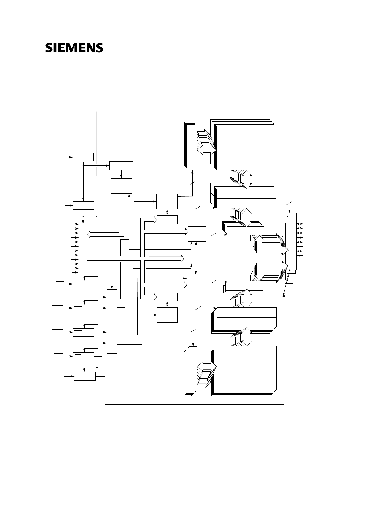
16MBit Synchronous DRAM
Row Decoder
Row Decoder
CKE
CLK
A0
A1
A2
A3
A4
A5
A6
A7
A8
A9
A10
A11 (BS)
CS
RAS
CAS
CKE Buffer
CLK Buffer
Address Buffers (12)
CS Buffer
RAS Buffer
CAS Buffer
Refresh Clock
12
12
Self
Row
Address
Counter
Command Decoder
Row/Column
Predecode A
11
11
Predecode B
Row/Column
Bank A
Select
Bank B
Select
3
Mode Register
11
3
8
8
Sequential
Control
Bank A
Sequential
Control
Bank B
8
8
2048
8
8
Memory Bank A
Sense Amplifiers
Sense Amplifiers
Column Decoder and DQ Gate
Column Decoder and DQ Gate
Data Latches
Data Latches
Data Latches
Column Decoder and DQ Gate
Sense Amplifiers
2048 x 512
1024
512
8
8
8
512
8
DQ0
DQ1
DQ2
DQ3
DQ4
8
8
DQ5
DQ6
DQ7
Data Input/Output Buffer s
WE
DQM
WE Buffer
DQM Buffer
2048
Row Decoder
Row Decoder
Memory Bank B
Block Diagram for HYB39S16800BT (2 banks x 1M x 8 SDRAM)
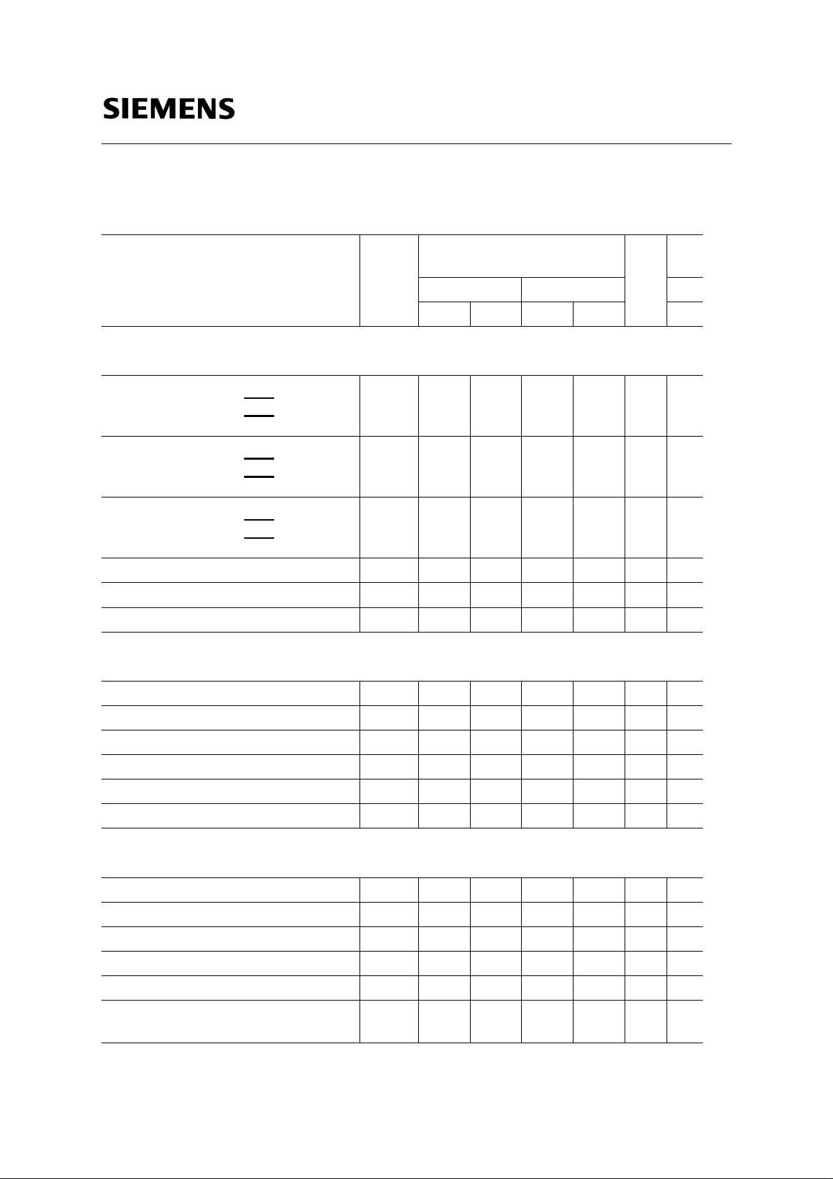
Semiconductor Group 6
Memory Bank B
2048 x 512
2048 x 1024
CKE
CLK
A0
A1
A2
A3
A4
A5
A6
A7
A8
A9
A10
A11 (BS)
CS
RAS
CAS
CKE Buffer
CLK Buffer
Addres s Buffers (12)
CS Buffer
RAS Buffer
CAS Buffer
Refresh Clock
12
12
Command Decoder
Self
Row
Address
Counter
Row/Column
Predecode A
11
11
Predecode B
Row/Column
Bank A
Select
Bank B
Select
Row Decoder
Row Decoder
3
Mode Register
11
Sequential
3
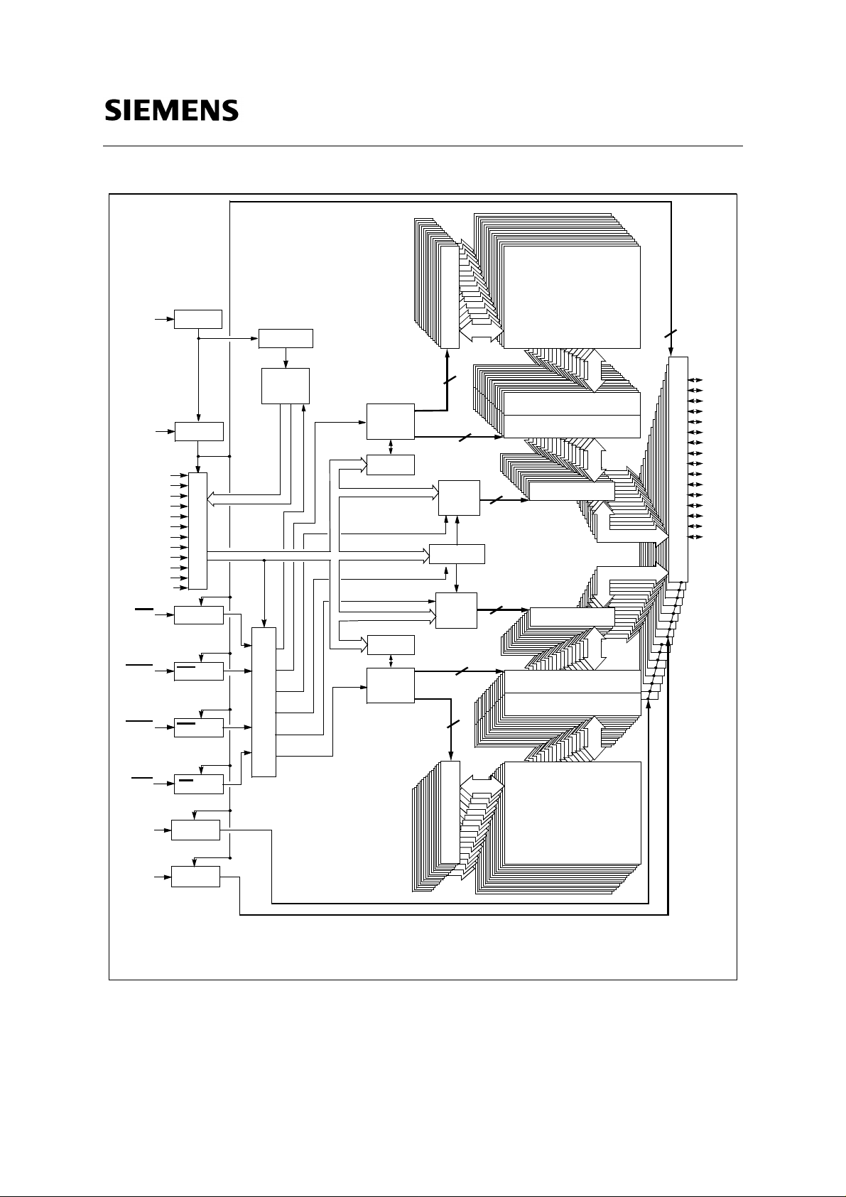
HYB39S16400/800/160BT-8/-10
16MBit Synchronous DRAM
Row Decoder
Row Decoder
16
16
Sequential
Control
Bank A
Control
Bank B
16
16
2048
Column Decoder and DQ Gate
2048 x 512
Memory Bank A
2048 x 256
Memory Bank A
1024
512
1024
256
Sense Amplifiers
Sense Amplifiers
Sense Amplifiers
Column Decoder and DQ Gate
16
16
Sense Amplifiers
Column Decoder and DQ Gate
Column Decoder and DQ Gate
8
8
8
Data Latches
Data Latches
Data Latches
Data Latches
Data Latches
Data Latches
Column Decoder and DQ Gate
Column Decoder and DQ Gate
Sense Amplifiers
Sense Amplifiers
8
8
256
8
8
16
DQ0
DQ1
DQ2
DQ3
DQ4
DQ5
DQ6
DQ7
DQ8
DQ9
DQ10
DQ11
DQ12
Data Input/Output Buffers
DQ13
DQ14
DQ15
WE
UDQM
LDQM
WE Buffer
DQM Buffer
DQM Buffer
2048
Memory Bank B
Memory Bank B
2048 x 256
Memory Bank B
2048 x 1024
Memory Bank B
Row Decoder
Row Dec o d e r
Row Decoder
Row Decoder
2048 x 512
2048 x 1024
Block Diagram for HYB39S16160BT (2 banks x 512k x 16 SDRAM)
Semiconductor Group 7
Operation Definition
HYB39S16400/800/160BT-8/-10
16MBit Synchronous DRAM
All of SDRAM operations are defined by states of control signals CS
, RAS, CAS, WE, and DQM at
the positive edge of the clock. The following list shows the most important operation commands.
Operation CS RAS CAS WE (L/U)DQM
Standby, Ignore RAS
Row Address Strobe and Activating a Bank L L H H X
Column Address Strobe and Read Command L H L H X
Column Address Strobe and Write Command L H L L X
Precharge Command L L H L X
Burst Stop Command L H H L X
Self Refresh Entry L L L H X
Mode Register Set Command L L L L X
Write Enable/Output Enable X X X X L
Write Inhibit/Output Disable X X X X H
No Operation (NOP) L H H H X
, CAS, WE and Address H X X X X
Mode Register
For application flexibility, a CAS
latency, a burst length, and a burst sequence can be
programmed in the SDRAM mode register. The mode set operation must be done before any
activate command after the initial power up. Any content of the mode register can be altered by reexecuting the mode set command. Both banks must be in precharged state and CKE must be high
at least one clock before the mode set operation. After the mode register is set, a Standby or NOP
command is required. Low signals of RAS
, CAS, and WE at the positive edge of the clock activate
the mode set operation. Address input data at this timing defines parameters to be set as shown in
the following table.
Semiconductor Group 8
HYB39S16400/800/160BT-8/-10
Address Input for Mode Set (Mode Register Operation)
BS
A10 A9
A8 A7 A6 A5
A3A4 A2 A1 A0
16MBit Synchronous DRAM
Address Bus (Ax)
Operation Mode
M11 M10 M9 M8 M7 Mode
0 0 0 0 0 Normal
X X100
CAS Latency
Operation Mode
Multiple Burst
with Single
Write
M6 M5 M4 Latency
0 0 0 Reserve
001 1
010 2
011 3
1 0 0 Reserve
1 0 1 Reserve
1 1 0 Reserve
1 1 1 Reserve
BT Burst LengthCAS Latency
Mode Register (Mx)
Burst Type
M3 Type
0 Sequential
1 Interleave
Burst Length
M2 M1 M0
000 1 1
001 2 2
010 4 4
011 8 8
1 0 0 Reserve Reserve
1 0 1 Reserve Reserve
1 1 0 Reserve Reserve
1 1 1 Full Page*) Reserve
Sequential Interleave
Length
*) optional
Sequential Burst Addressing Interleave Burst Addressing
0 1 2 3 4 5 6 7
1 2 3 4 5 6 7 0
2 3 4 5 6 7 0 1
3 4 5 6 7 0 1 2
4 5 6 7 0 1 2 3
5 6 7 0 1 2 3 4
6 7 0 1 2 3 4 5
7 0 1 2 3 4 5 6
Semiconductor Group 9
0 1 2 3 4 5 6 7
1 0 3 2 5 4 7 6
2 3 0 1 6 7 4 5
3 2 1 0 7 6 5 4
4 5 6 7 0 1 2 3
5 4 7 6 1 0 3 2
6 7 4 5 2 3 0 1
7 6 5 4 3 2 1 0

Read and Write Access Mode
HYB39S16400/800/160BT-8/-10
16MBit Synchronous DRAM
When RAS
starts. According to address data, a word line of the selected bank is activated and all of sense
amplifiers associated to the word line are fired. A CAS cycle is triggered by setting RAS
CAS
low at a clock timing after a necessary delay, tRCD, from the RAS timing. WE is used to define
either a read (WE
SDRAM provides a wide variety of fast access modes. In a single CAS cycle, serial data read
or write operations are allowed at up to a 125 MHz data rate. The numbers of serial data bits are the
burst length programmed at the mode set operation, i.e., one of 1, 2, 4, 8 and full page, where full
page is an optional feature in this device. Column addresses are segmented by the burst length and
serial data accesses are done within this boundary. The first column address to be accessed is
supplied at the CAS timing and the subsequent addresses are generated automatically by the
programmed burst length and its sequence. For example, in a burst length of 8 with interleave
sequence, if the first address is ‘2’, then the rest of the burst sequence is 3, 0, 1, 6, 7, 4, and 5 .
Full page burst operation is only possible using the sequential burst type and page length is
a function of the I/O organisation and column addressing. Full page burst operation do not self
terminate once the burst length has been reached. In other words, unlike burst length of 2, 3 or 8,
full page burst continues until it is terminated using another command.
Similar to the page mode of conventional DRAM’s, burst read or write accesses on any column
address are possible once the RAS cycle latches sense amplifiers. The maximum tRAS or the
refresh interval time limits the number of random column accesses. A new burst access can be
done even before the previous burst ends. The interrupt operation at every clock cycles is
supported. When the previous burst is interrupted, the remaining addresses are overridden by the
new address with the full burst length. An interrupt which accompanies with an operation change
from a read to a write is possible by exploiting DQM to avoid bus contention.
is low and both CAS and W E are high at the positive edge of the clock, a RAS cycle
high and
= H) or a write (WE = L) at this stage.
When two banks are activated sequentially, interleaved bank read or write operations are
possible. With the programmed burst length, alternate access and precharge operations on two
banks can realize fast serial data access modes among many different pages. Once two banks are
activated, column to column interleave operation can be done between two different pages.
Refresh Mode
SDRAM has two refresh modes, a CAS before RAS (CBR) automatic refresh and a self refresh.
All of banks must be precharged before applying any refresh mode. An on-chip address counter
increments the word and the bank addresses and no bank information is required for both refresh
modes. The chip enters the automatic refresh mode, when RAS
WE
are held high at a clock timing. The mode restores word line after the refresh and no external
precharge command is necessary. A minimum tRC time is required between two automatic
refreshes in a burst refresh mode. The same rule applies to any access command after the
automatic refresh operation.
The chip has an on-chip timer and the self refresh mode is available. It enters the mode when
RAS
, CAS, and CKE are low and WE is high at a clock timing. All of external control signals
including the clock are disabled. Returning CKE to high enables the clock and initiates the refresh
exit operation. After the exit command, at least one tRC delay is required prior to any access
command.
Semiconductor Group 10
and CAS are held low and CKE and

HYB39S16400/800/160BT-8/-10
16MBit Synchronous DRAM
DQM Function
DQM has two functions for data I/O read write operations. During reads, when it turns to high
at a clock timing, data outputs are disabled and become high impedance after two clock delay (DQM
Data Disable Latency t
activated, the write operation at the next clock is prohibited (DQM Write Mask Latency t
clocks).
Suspend Mode
During normal access mode, CKE is held high and CLK is enabled. When CKE is low, it freezes
the internal clock and extends data read and write operations. One clock delay is required for mode
entry and exit (Clock Suspend Latency t
Power Down
In order to reduce standby power consumption, a power down mode is available. Bringing CKE
low enters the power down mode and all of receiver circuits are gated. All banks must be
precharged before entering this mode. One clock delay is required for mode entry and exit. The
Power Down mode does not perform any refresh operation.
). It also provides a data mask function for writes. When DQM is
DQZ
DQW
).
CSL
= zero
Auto Precharge
Two methods are available to precharge SDRAMs. In an automatic precharge mode, the CAS
timing accepts one extra address, CA10, to determine whether the chip restores or not after the
operation. If CA10 is high when a Read Command is issued, the Read with Auto-Precharge
function is initiated. The SDRAM automatically enters the precharge operation one clock after the
Read Command is registered for CAS
latencies of 1 and 2, and two clocks for CAS latencies of 3.
If CAS10 is high when a Write Command is issued, the Write with Auto-Precharge function is
initiated. The SDRAM automatically enters the precharge operation one clock delay form the last
data-in for CAS
as t
DPL
.
latencies of 1 and 2 and two clocks for CAS latencies of 3. This delay is referenced
Precharge Command
If CA10 is low, the chip needs another way to precharge. In this mode, a separate precharge
command is necessary. When RAS
and WE are low and CAS is high at a clock timing, it triggers the
precharge operation. Two address bits, A10 and A11, are used to define banks as shown in the
following list. The precharge command may be applied coincident with the last of burst reads for
CAS Latency = 1 and with the second to the last read data for CAS Latencies = 2 & 3. Writes require
a time t
A10 A11
Bank A Only Low Low
Bank B Only Low High
Both A and B High Don’t Care
from the last burst data to apply the precharge command.
DPL
Bank Selection by Address Bits
Semiconductor Group 11

HYB39S16400/800/160BT-8/-10
16MBit Synchronous DRAM
Burst Termination
Once a burst read or write operation has been initiated, there are several methods in which to
terminate the burst operation prematurely. These methods include using another Read or Write
Command to interrupt an existing burst operation, use a Precharge Command to interrupt a burst
cycle and close the active bank, or using the Burst Stop Command to terminate the existing burst
operation but leave the bank open for future Read or Write Commands to the same page of the
active bank. When interrupting a burst with another Read or Write Command care must be taken to
avoid DQ contention. The Burst Stop Command, however, has the fewest restrictions making it the
easiest method to use when terminating a burst operation before it has been completed. If a Burst
Stop command is issued during a burst write operation, then any residual data from the burst write
cycle will be ignored. Data that is presented on the DQ pins before the Burst Stop Command is
registered will be written to the memory.
Power Up Procedure
All Vdd and Vddq must reach the specified voltage no later than any of input signal voltages. An
initial pause of 200 µsec is required after power on. All banks have to be precharged and a minimum
of 2 auto-refresh cycles are required prior to the mode register set operation.
Semiconductor Group 12
HYB39S16400/800/160BT-8/-10
16MBit Synchronous DRAM
Absolute Maximum Ratings
Operating temperature range .........................................................................................0 to + 70 °C
Storage temperature range......................................................................................– 55 to + 150 °C
Input/output voltage .............................................................................. – 0.5 to min(Vcc+0.5, 4.6) V
Power supply voltage VDD / VDDQ.......................................................................... – 1.0 to + 4.6 V
Power Dissipation............................................. ..........................................................................1 W
Data out current (short circuit) ................................................................................................ 50 mA
Note:
Stresses above those listed under “Absolute Maximum Ratings” may cause permanent
damage of the device. Exposure to absolute maximum rating conditions for extended periods
DD,VDDQ
= 3.3 V ± 0.3 V
may affect device reliability.
Recommended Operation and Characteristics for LV-TTL versions:
T
= 0 to 70 °C; VSS = 0 V; V
A
Parameter Symbol Limit Values Unit Notes
min. max.
Input high voltage
Input low voltage
I
Output high voltage (
Output low voltage (
= – 2.0 mA) V
OUT
I
= 2.0 mA) V
OUT
Input leakage current, any input
V
(0 V <
< Vddq, all other inputs = 0 V)
IN
Output leakage current
(DQ is disabled, 0 V <
V
OUT
< VCC)
V
V
I
I
IH
IL
OH
OL
I(L)
O(L)
2.0 Vcc+0.3 V 1, 2, 3
– 0.3 0.8 V 1, 2, 3
2.4 – V 3
– 0.4 V 3
– 10 10 µA
– 10 10 µA
Notes:
1. All voltages are referenced to VSS.
2. Vih may overshoot to Vcc + 2.0 V for pulse width of < 4ns with 3.3V. Vil may undershoot to
-2.0 V for pulse width < 4.0 ns with 3.3V. Pulse width measured at 50% points with amplitude measured peak
to DC reference.
Capacitance
T
= 0 to 70 °C; V
A
= 3.3 V ± 0.3 V, f = 1 MHz
DD
Parameter Symbol Values Unit
Input capacitance
(CLK) C
Input capacitance
(A0-A12, BA0,BA1,RAS, CAS, WE, CS, CKE, DQM)
Input / Output capacitance
(DQ) C
Semiconductor Group 13
min. max.
I1
C
I2
IO
2.5 4.0 pF
2.5 5.0 pF
4.0 6.5 pF
Operating Currents (TA = 0 to 70oC, VCC = 3.3V ± 0.3V
(Recommended Operating Conditions unless otherwise noted)
HYB39S16400/800/160BT-8/-10
16MBit Synchronous DRAM
Parameter
Symbol
Operating Current Icc1
Precharge
Icc2P
Standby Current
in Power Down
Icc2PS
Mode
Precharge
Icc2N
Standby Current
in Non-power
down Mode
Active Standby
Icc2NS
Icc3P
Current in Power
Down Mode
Active Standby
Icc3PS
Icc3N
Current in Nonpower Down
Mode
Icc3NS
Burst Operating
Current
Auto (CBR)
Refresh Current
Self Refresh Icc6
Icc4
Icc5
Test Condition CAS
Burst Length = 4
trc>=trc (min.)
tck>=tck(min.), Io = 0mA
2 bank interleave operation
CKE<=VIL(max),
tck>=tck(min.)
CKE<=VIL(max),
tCK=infinite
CKE>=VIH(min),
tck>=tck(min.) input signals
changed once in 3 cycles
CKE>=VIH(min),
tCK=infinite, input signals
are stable
CKE<=VIL(max),
tck>=tck(min.)
CKE<=VIL(max),
tCK=infinite, inpit signals
are stable
CKE>=VIH(min),
tck>=tck(min.),
changed once in 3 cycles
CKE>=VIH(min),
tCK=infinite, input signals
are stable
Burst Length = full page
trc = infinite
tck >= tck (min.), IO = 0 mA
2 banks activated
trc>=trc(min)
CKE=<0,2V
Latency
1
2
3
1
2
3
1
2
3
-8 -10
max. max.
80
115
125
65
90
100
mA
mA
mA
33 mA
22mA
20 20 mA
10 10 mA
33mA
22mA
25 25 mA
15 15 mA
50
80
120
75
95
115
11mA1, 2
40
mA 1, 2
65
95
60
mA
75
mA
90
mA
1
Note
1, 2
CS=
High
CS=
High,
1
1, 2
Notes:
1. The specified values are valid when addresses are changed no more than three times during trc(min.) and
when No Operation commands are registered on every rising clock edge during tRC(min).
2. The specified values are valid when data inputs (DQ’s) are stable during tRC(min.).
Semiconductor Group 14
AC Characteristics 1)2)3)
T
= 0 to 70 °C; VSS = 0 V; VCC = 3.3 V ± 0.3 V, t
A
= 1 ns
T
HYB39S16400/800/160BT-8/-10
16MBit Synchronous DRAM
Parameter
Clock and Clock Enable
Clock Cycle Time
CAS
CAS
Clock Frequency
CAS
CAS
Access Time from Clock
CAS
CAS
Clock High Pulse Width
Clock Low Pulse Width
Transition time
Latency = 3
Latency = 2
Latency = 3
Latency = 2
Latency = 3
Latency = 2
Symbol
t
CK
t
CK
t
AC
t
CH
t
CL
t
T
Limit Values
Unit
-8 -10
min max min max
s
8
10
–
–
–
–
–
–
125
100
6
6
10
12
–
–
–
–
–
ns
–
ns
10075MHz
MHz
78ns
ns
3–3–ns
3–3–ns
0.5 10 0.5 10 ns
2, 4
Setup and Hold Times
Input Setup Time t
Input Hold Time t
CKE Setup Time t
CKE Hold Time t
Mode Register Set-up time t
Power Down Mode Entry Time
Common Parameters
Row to Column Delay Time t
Row Active Time t
Row to Column Delay Time t
Row Precharge Time t
Row Cycle Time t
Activate(a) to Activate(b) Command
period
t
t
IS
IH
CKS
CKH
RSC
SB
RCD
RAS
RCD
RP
RC
RRD
2–3–ns
1–1–ns
2–3–ns
1–1–ns
16 – 20 – ns
08010ns
20 – 24 – ns
45
100k
60
100k
ns
20 – 24 – ns
20 – 24 – ns
70
–
90
–
ns
16 – 20 – ns
5
5
5
5
6
6
6
6
6
6
Semiconductor Group 15
HYB39S16400/800/160BT-8/-10
16MBit Synchronous DRAM
Parameter
(a) to CAS(b) Command period t
CAS
Refresh Cycle
Refresh Period
(4096 cycles)
Self Refresh Exit Time
Read Cycle
Data Out Hold Time t
Data Out to Low Impedance Time
Data Out to High Impedance Time
DQM Data Out Disable Latency
Symbol
CCD
t
REF
t
SREX
OH
t
LZ
t
HZ
t
DQZ
Limit Values
Unit
-8 -10
min max min max
1–1–CLK
–64–64ms
10 10 ns
3–3–ns2
0–0–ns
38310ns
8
2–2–CLK
Write Cycle
Write Recovery Time t
DQM Write Mask Latency
Write Latency
WR
t
DQW
t
WL
Frequency vs. AC Parameter Relationship Table:
-8 -parts
CL tRC tRAS tRP tRRD tRCD tCCD
125 MHz 3 9 6 3 2 3 1 0 1
100 MHz 2 7 5 2 2 2 1 0 1
-10 -parts:
CL tRC tRAS tRP tRRD tRCD tCCD WL tWR
100 MHz 3 8 6 3 2 3 1 0 1
75 MHz 2 7 5 2 2 2 1 0 1
8–10–ns
0–0–CLK
0–0–CLK
t
WL
tWR
Semiconductor Group 16
HYB39S16400/800/160BT-8/-10
16MBit Synchronous DRAM
Notes for AC Parameters:
1. For proper power-up see the operation section of this data sheet.
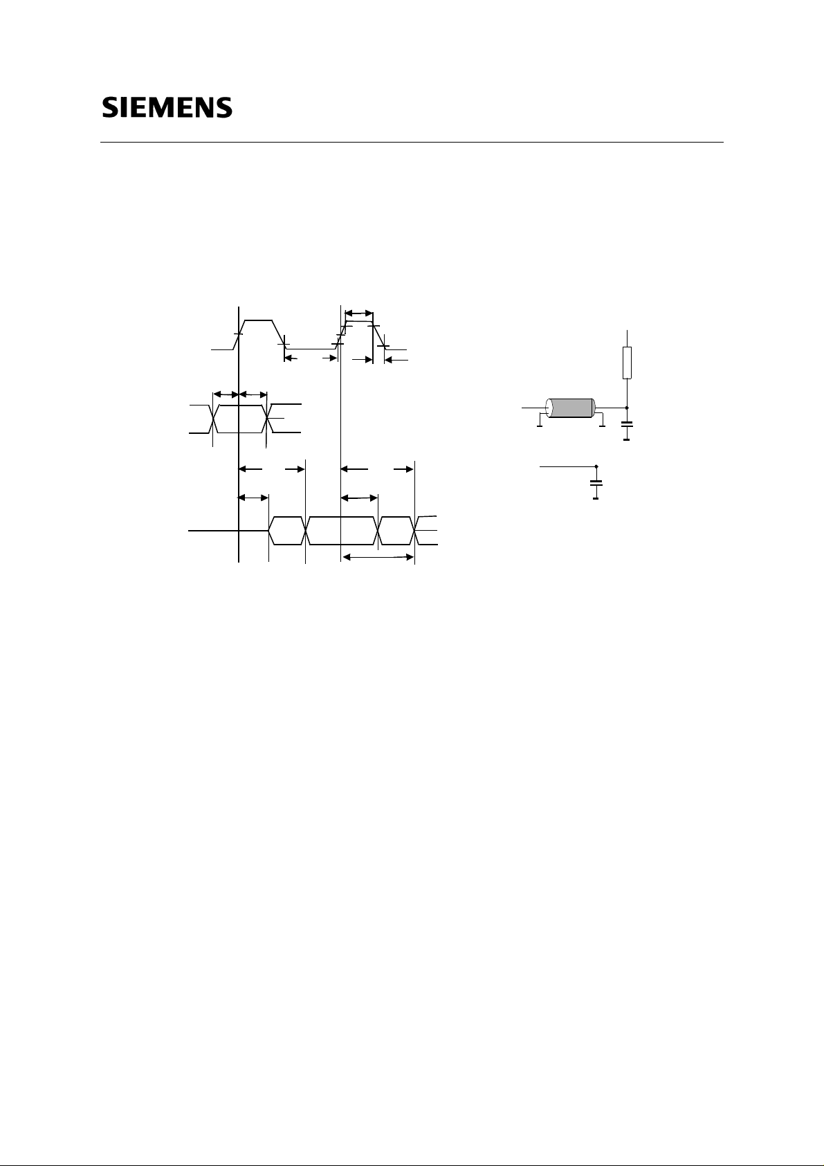
2. AC timing tests for LV-TTL versions have V
crossover point. The transition time is measured between V
with the AC output load circuit shown in fig.1. Specified tac and toh parameters are measured with a 50 pF only,
without any resistive termination and with a input signal of 1V / ns edge rate between 0.8V and 2.0 V.
CLOCK
tCL
tSETUP tHOLD
INPUT
1.4V
= 0.4 V and Vih = 2.4 V with the timing referenced to the 1.4 V
tCH
il
2.4 V
0.4 V
t
T
and Vil. All AC measurements assume tT=1ns
ih
Z=50 Ohm
I/O
+ 1.4 V
50 Ohm
50 pF
tLZ
tAC
tAC
tOH
I/O
50 pF
Measurement conditions for
OUTPUT
3. If clock rising time is longer than 1 ns, a time (t
4. If tT is longer than 1 ns, a time (t
-1) ns has to be added to this parameter.
T
1.4V
tHZ
/2 - 0.5) ns has to be added to this parameter.
T
fig.1
tac and toh
5. These parameter account for the number of clock cycle and depend on the operating frequency of the clock,
as follows:
the number of clock cycle = specified value of timing period (counted in fractions as a whole number)
Self Refresh Exit is a synchronous operation and begins on the 2nd positive clock edge after CKE returns high.
Self Refresh Exit is not complete until a time period equal to tRC is satisfied once the Self Refresh Exit
command is registered.
Semiconductor Group 17
Package Outlines:
x
Plastic Package P-TSOPII-44 ( 400mil, 0.8mm lead pitch)
Thin small outline package, SMD
HYB39S16400/800/160BT-8/-10
16MBit Synchronous DRAM
GLX05862
Plastic Package P-TSOPII-50 ( 400mil, 0.8mm lead pitch)
Thin small outline package, SMD
-
+0.05
-
+0.05
1
1.2 ma
0.1
0.8
+0.05
0.4
-0.1
M
0.2 50x
0.1
50 26
125
1)
+0.13
20.95
Index marking
-
TSOP-44 (400).WMF
+0.13
10.16
-
+0.1
0.5
-
+0.2
11.76
-
-0.03
+0.06
0.15
1) Does not include plastic or metal protusion of 0.25 max. per side
Semiconductor Group 18

Timing Diagrams
1. Bank Activate Command Cycle
2. Burst Read Operation
3. Read Interrupted by a Read
4. Read to Write Interval
4.1 Read to Write Interval
4.2 Minimum Read to Write Interval
4.3 Non-Minimum Read to Write Interval
5. Burst Write Operation
6. Write and Read Interrupt
6.1 Write Interrupted by a Write
6.2 Write Interrupted by Read
7. Burst Read & Write with Auto-Precharge
7.1 Burst Write with Auto Precharge
7.2 Burst Read with Auto Precharge
8. Burst Termination
8.1 Termination of a Burst Read Operation
8.2 Termination of a Burst Write Operation
9. AC- Parameters
9.1 AC Parameters for a Write Timing
9.2 AC Parameters for a Read Timing
10. Mode Register Set
11. Power on Sequence and Auto Refresh (CBR)
12. Clock Suspension (using CKE)
12.1 Clock Suspension During Burst Read CAS
12. 2 Clock Suspension During Burst Read CAS
12. 3 Clock Suspension During Burst Read CAS
12. 4 Clock Suspension During Burst Write CAS
12. 5 Clock Suspension During Burst Write CAS
12. 6 Clock Suspension During Burst Write CAS
13. Power Down Mode and Clock Suspend
14. Auto Refresh (CBR)
15. Self Refresh ( Entry and Exit)
16. Random Column Read ( Page within same Bank)
16.1 CAS
16.2 CAS
16.3 CAS
17. Random Column Write ( Page within same Bank)
17.1 CAS
17.2 CAS
17.3 CAS
Latency = 1
Latency = 2
Latency = 3
Latency = 1
Latency = 2
Latency = 3
HYB39S16400/800/160BT-8/-10
16MBit Synchronous DRAM
Latency = 1
Latency = 2
Latency = 3
Latency = 1
Latency = 2
Latency = 3
Semiconductor Group 19
Timing Diagrams (cont’d)
18. Random Row Read ( Interleaving Banks)
18.1 CAS
18.2 CAS
18.3 CAS
19. Random Row Write ( Interleaving Banks)
19.1 CAS
19.2 CAS
19.3 CAS
20. Full Page Read Cycle (optional feature)
20.1 CAS
20.2 CAS
20.3 CAS
21. Full Page Write Cycle (optional feature)
21.1 CAS Latency = 1
21.2 CAS
21.3 CAS
22. Precharge Termination of a Burst
22.1 CAS
22.2 CAS
22.3 CAS
Latency = 1
Latency = 2
Latency = 3
Latency = 1
Latency = 2
Latency = 3
Latency = 1
Latency = 2
Latency = 3
Latency = 2
Latency = 3
Latency = 1
Latency = 2
Latency = 3
HYB39S16400/800/160BT-8/-10
16MBit Synchronous DRAM
Semiconductor Group 20
 Loading...