

Siemens HYB39S16400AT-10, HYB39S16400AT-8, HYB39S16800AT-10, HYB39S16800AT-8, HYB39S16160AT-10 Datasheet
...
16 MBit Synchronous DRAM
(second generation)
Advanced Information
HYB 39S16400/800/160AT-8/-10
• High Performance:
latency = 3 -8 -10 Units
CAS
f
CK
t
CK3
t
AC3
• Single Pulsed RAS
• Fully Synchronous to Positive Clock Edge
• 0 to 70 °C operating temperature
• Dual Banks controlled by A11 (Bank Select)
• Programmable CAS
• Programmable Wrap Sequence: Sequential
or Interleave
• Programmable Burst Length:
1, 2, 4, 8 and full page for Sequential type
1, 2, 4, 8 for Interleave type
125 100 MHz
810ns
78ns
Interface
Latency: 1, 2, 3
• Multiple Burst Read with Single Write
Operation
• Automatic and Controlled Precharge
Command
• Data Mask for Read/Write control (× 4, × 8)
• Dual Data Mask for byte control (× 16)
• Auto Refresh (CBR) and Self Refresh
• Suspend Mode and Power Down Mode
• 4096 refresh cycles/64 ms
• Random Column Address every CLK
(1-N Rule)
• Single 3.3 V ± 0.3 V Power Supply
• LVTTL Interface versions
• Plastic Packages:
P-TSOPII-44-1 400 mil width (× 4, × 8)
P-TSOPII-50-1 400 mil width (× 16)
The HYB 39S1640x/80x/16xAT are dual bank Synchrono us DRAM’s based on the die revi sions “B”
and “C” and organized as 2 banks × 2MBit× 4, 2 banks × 1MBit× 8 and 2 banks × 512 kBit × 16
respectively. These synchronous devices achiev e high speed data transfer rates up to 125 M Hz by
employing a chip architecture that prefetches m ultiple bits and then sy nchronizes the ou tput data to
a system clock. The chip is fabric ated with SIEMENS advanced 16 MBit DRAM process techn ology.
The device is designed to comply with all JEDEC standards set for synchronous DRAM products,
both electrically and mechanically. All of the control, address, data input and output circuits are
synchronized with the positive edge of an externally supplied clock.
Operating the two memory banks in an interleaved fashion allows random access operation to occur
at higher rate than is possible with standard DRAMs. A sequential and gapless data rate of up to
125 MHz is possible depending on burst length, CAS
Auto Refresh (CBR) and Self Refresh operation are supported. These devices operate with a single
3.3 V ± 0.3 V power supply and are available in TSOPII packages.
latency and speed grade of the device.
Semiconductor Group 1 1998-10-01
HYB 39S16400/800/160AT-8/-10
16 MBit Synchronous DRAM
Ordering Information
Type Ordering Code Package Description
LVTTL-Version
HYB 39S16400AT-8 Q67100-Q1333 P-TSOPII-44-1 (400 mil) 125 MHz 2B × 2 M × 4 SDRAM
PC66 2-2-2
HYB 39S16400AT-10 Q67100-Q1323 P-TSOPII-44-1 (400 mil) 100 MHz 2B × 2 M × 4 SDRAM
PC66 2-2-2
HYB 39S16800AT-8 Q67100-Q1335 P-TSOPII-44-1 (400 mil) 125 MHz 2B × 1 M × 8 SDRAM
PC66 2-2-2
HYB 39S16800AT-10 Q67100-Q1327 P-TSOPII-44-1 (400 mil) 100 MHz 2B × 1 M × 8 SDRAM
PC66 2-2-2
HYB 39S16160AT-8 Q67100-Q1337 P-TSOPII-50-1 (400 mil) 125 MHz 2B × 512 k × 16 SDRAM
HYB 39S16160AT-10 Q67100-Q1331 P-TSOPII-50-1 (400 mil) 100 MHz 2B × 512 k × 16 SDRAM
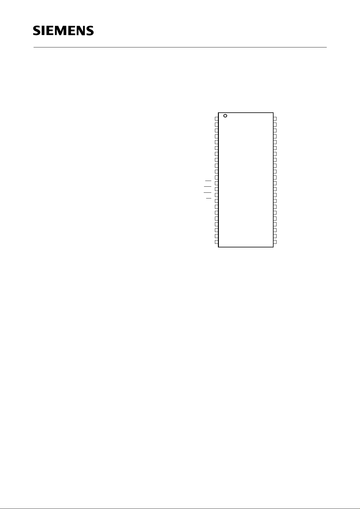
Pin Names
CLK Clock Input DQ Data Input/Output
CKE Clock Enable DQM, LDQM,
Data Mask
UDQM
CS
RAS
CAS
WE
Chip Select V
Row Address Strobe V
Column Address Strobe V
Write Enable V
DD
SS
DDQ
SSQ
Power (+ 3.3 V)
Ground
Power for DQ’s (+ 3.3 V)
Ground for DQ’s
A0 - A10 Address Inputs NC Not connected
A11 (BS) Bank Select
Semiconductor Group 2 1998-10-01
HYB 39S16400/800/160AT-8/-10
16 MBit Synchronous DRAM
V
DQ0
V
SSQ
DQ1
V
DDQ
DQ2
V
SSQ
DQ3
V
DDQ
N.C.
N.C.
WE
CAS
RAS
A11
A10
V
CS
A0
A1
A2
V
1
DD
2
3
4
5
6
7
8
9
10
11
12
13
14
15
16
17
18
19
20
21
22
DD
44
43
42
41
40
39
38
37
36
35
34
33
32
31
30
29
28
27
26
25
24
23
SPP03402
SS
DQ7
V
SSQ
DQ6
V
DDQ
DQ5
V
SSQ
DQ4
V
DDQ
N.C.
N.C.
DQM
CLK
CKE
N.C.
A9
A8
A7
A6
A5
A4A3
V
SS
Pin Configuration
Semiconductor Group 3 1998-10-01
Signal Pin Description
Pin Type Signal Polarity Function
HYB 39S16400/800/160AT-8/-10
16 MBit Synchronous DRAM
CLK Input Pulse Positive
Edge
CKE Input Level Active
High
CS
RAS
CAS
WE
A0 - A10 Input Level – During a Bank Activate command cycle, A0 - A10 defines
Input Pulse Active
Low
Input Pulse Active
Low
The system clock input. All of the SDRAM inputs are
sampled on the rising edge of the clock.
Activates the CLK signal when high and deactivates the
CLK signal when low, thereby initiates either the Power
Down mode, Suspend mode or the Self Refresh mode.
CS enables the command decoder when low and disables
the command decoder when high. When the command
decoder is disabled, new commands are ignored but
previous operations continue.
When sampled at the positive rising edge of the clock,
, RAS and WE define the command to be executed by
CAS
the SDRAM.
the row address (RA0 - RA10) when sampled at the rising
clock edge.
During a Read or Write command cycle, A0 - A9 defines
the column address (CA0 - CAn) when sampled at the
rising clock edge. CAn depends from the SDRAM
organisation.
4M × 4 SDRAM CAn = CA9
2M × 8 SDRAM CAn = CA8
1M × 16 SDRAM CAn = CA7
In addition to the column address, A10 is used to invoke
autoprecharge operation at the end of the burst read or
write cycle. If A10 is high, autoprecharge is selected and
A11 defines the bank to be precharged (low = bank A,
high = bank B). If A10 is low, autoprecharge is disabled.
During a Precharge command cycle, A10 is used in
conjunction with A11 to control which bank(s) to
precharge. If A10 is high, both bank A and bank B will be
precharged regardless of the state of A11. If A10 is low,
then A11 is used to define which bank to precharge.
A11 (BS) Input Level – Selects which bank is to be active. A11 low selects bank A
and A11 high selects bank B.
DQx Input
Output
Semiconductor Group 4 1998-10-01
Level – Data Input/Output pins operate in the s ame manner as on
conventional DRAMs.
Signal Pin Description (cont’d)
Pin Type Signal Polarity Function
HYB 39S16400/800/160AT-8/-10
16 MBit Synchronous DRAM
DQM
LDQM
UDQM
V
DD
V
SS
V
DDQ
V
SSQ
Input Pulse Active
High
The Data Input/Output mask places the DQ buffers in a
high impedance state when sampled high. In Read mode,
DQM has a latency of two clock cycles and controls the
output buffers like an output enable. I n Write m ode, DQM
has a latency of zero and operates as a word mask by
allowing input data to be written if it is low but blocks the
write operation if DQM is high.
Supply – – Power and ground for the input buffers and the core logic.
Supply – – Isolated power supply and ground for the output buffe rs to
provide improved noise immunity.
Semiconductor Group 5 1998-10-01
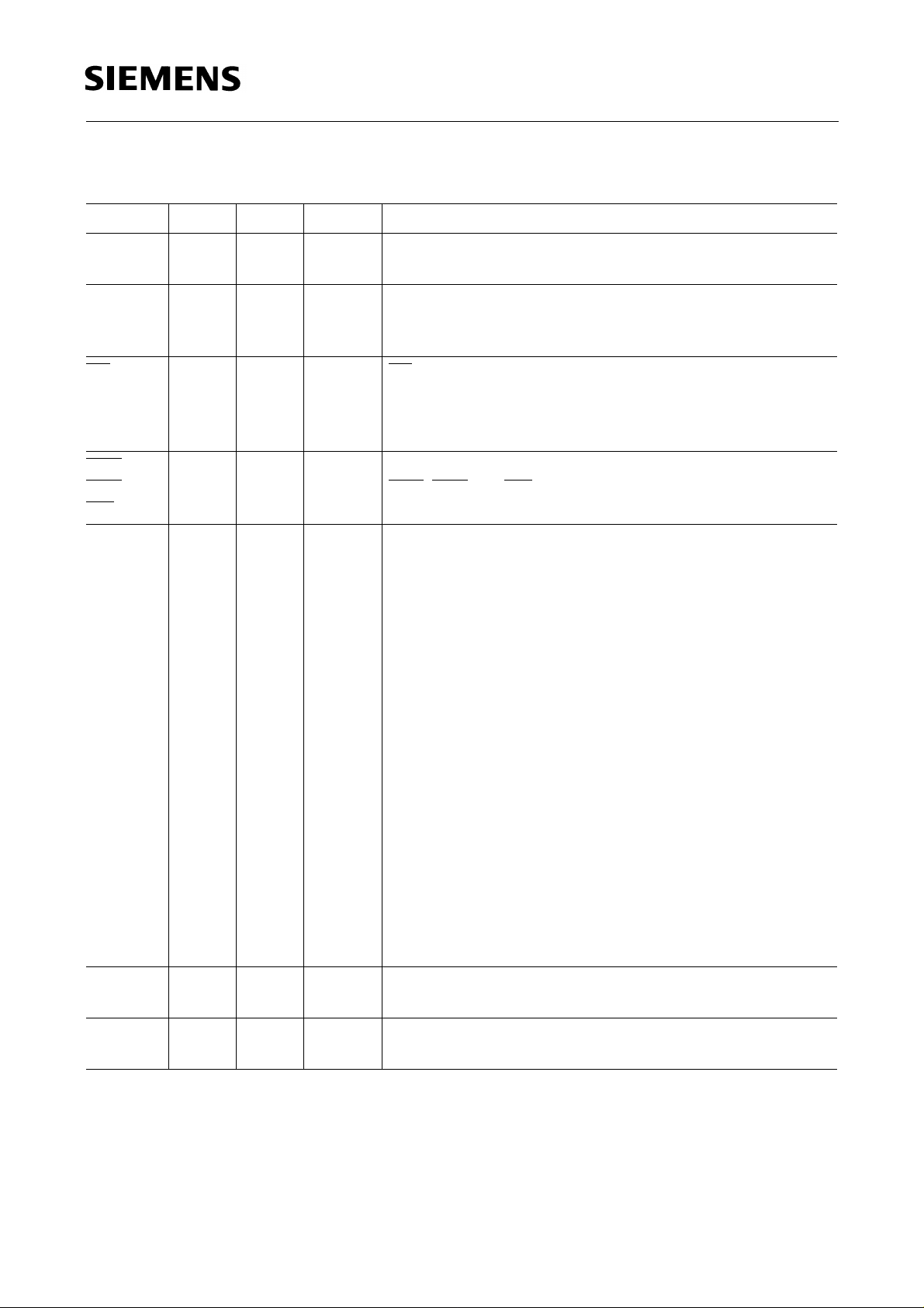
HYB 39S16400/800/160AT-8/-10
16 MBit Synchronous DRAM
CKE
CLK
A0
A1
A2
A3
A4
A5
A6
A7
A8
A9
A10
A11 (BS)
CS
RAS
CAS
WE
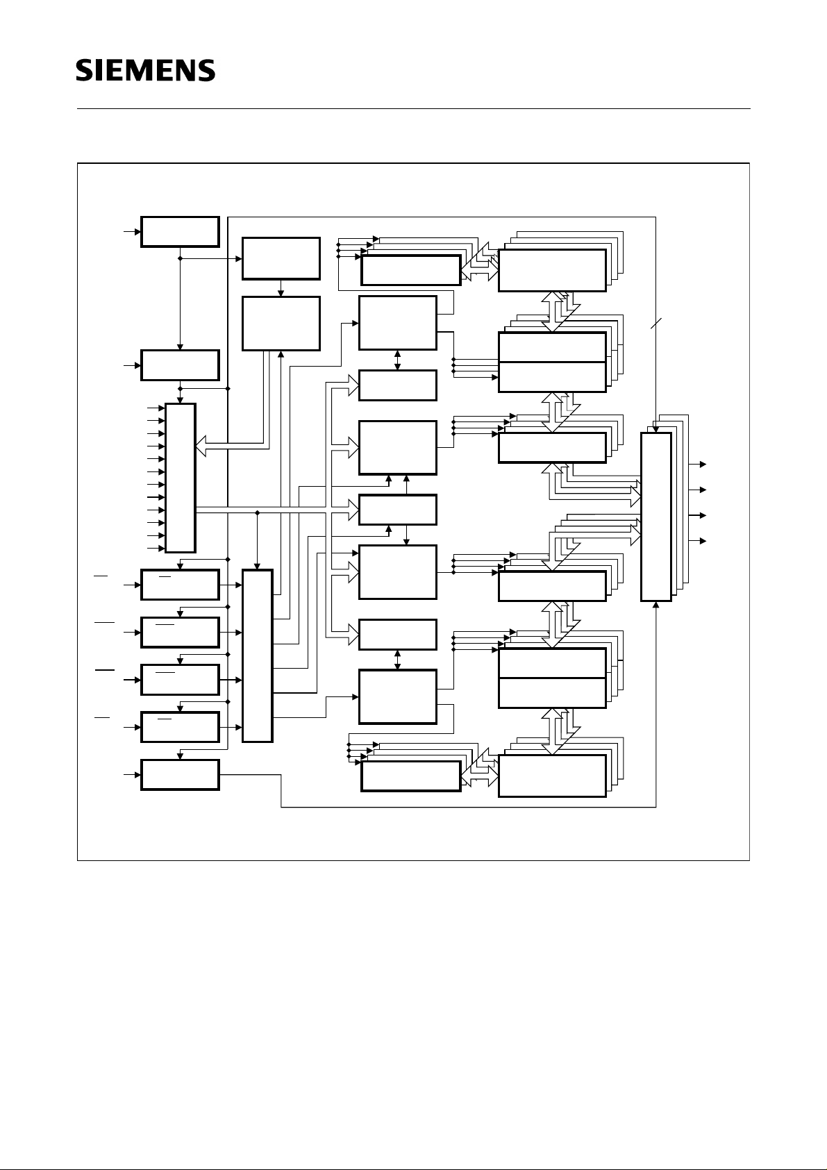
CKE Buffer
CLK Buffer
12
12
Address Buffers (12)
CS Buffer
RAS Buffer
CAS Buffer
WE Buffer
Self
Refresh Clock
Row
Address
Counter
Command Decoder
Row/Column
11
Predecode A
3
11
Mode Register
3
11
Predecode B
Row/Column
Row Decoder
Bank A
Select
Sequential
Control
Bank A
Sequential
Control
Bank B
Bank B
Select
2048
2048 x 1024
Memory Bank A
1024
Sense Amplifiers
Column Decoder
and DQ Gate
8
Data Latches
8
8
Data Latches
8
Column Decoder
and DQ Gate
Sense Amplifiers
1024
4
DQ0
DQ1
DQ2
DQ3
Data Input/Output Buffers
DQM
DQM Buffer
Row Decoder
2048
Memory Bank B
2048 x 1024
SPB02835
Block Diagram for HYB 39S16400T (2 banks × 4 M × 4 SDRAM)
Semiconductor Group 6 1998-10-01
HYB 39S16400/800/160AT-8/-10
16 MBit Synchronous DRAM
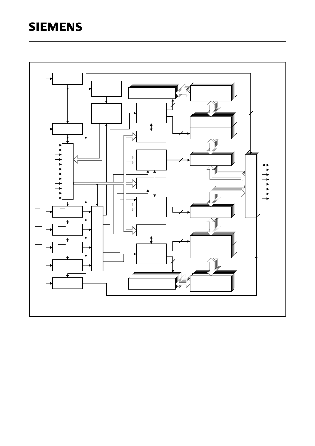
CKE
CLK
A0
A1
A2
A3
A4
A5
A6
A7
A8
A9
A10
A11 (BS)
CS
RAS
CAS
WE
CKE Buffer
CLK Buffer
12
12
Address Buffers (12)
CS Buffer
RAS Buffer
CAS Buffer
WE Buffer
Self
Refresh Clock
Row
Address
Counter
Command Decoder
Row/Column
11
Predecode A
3
11
Mode Register
3
11
Predecode B
Row/Column
Row Decoder
Bank A
Select
Sequential
Control
Bank A
Sequential
Control
Bank B
Bank B
Select
2048
8
8
8
8
8
8
2048 x 512
Memory Bank A
512
Sense Amplifiers
Column Decoder
and DQ Gate
8
Data Latches
8
8
Data Latches
8
Column Decoder
and DQ Gate
Sense Amplifiers
512
8
DQ0
DQ1
DQ2
DQ3
DQ4
DQ5
DQ6
DQ7
Data Input/Output Buffers
DQM
DQM Buffer
Row Decoder
2048
Memory Bank B
2048 x 512
SPB02836
Block Diagram for HYB 39S16800T (2 banks × 1 M × 8 SDRAM)
Semiconductor Group 7 1998-10-01
 Loading...