Siemens HYB39S16160CT-6, HYB39S16160CT-7 Datasheet
1M x 16 MBit Synchronous DRAM
for High Speed Graphics Applications
HYB39S16160CT-6/-7
16MBit Synchronous DRAM
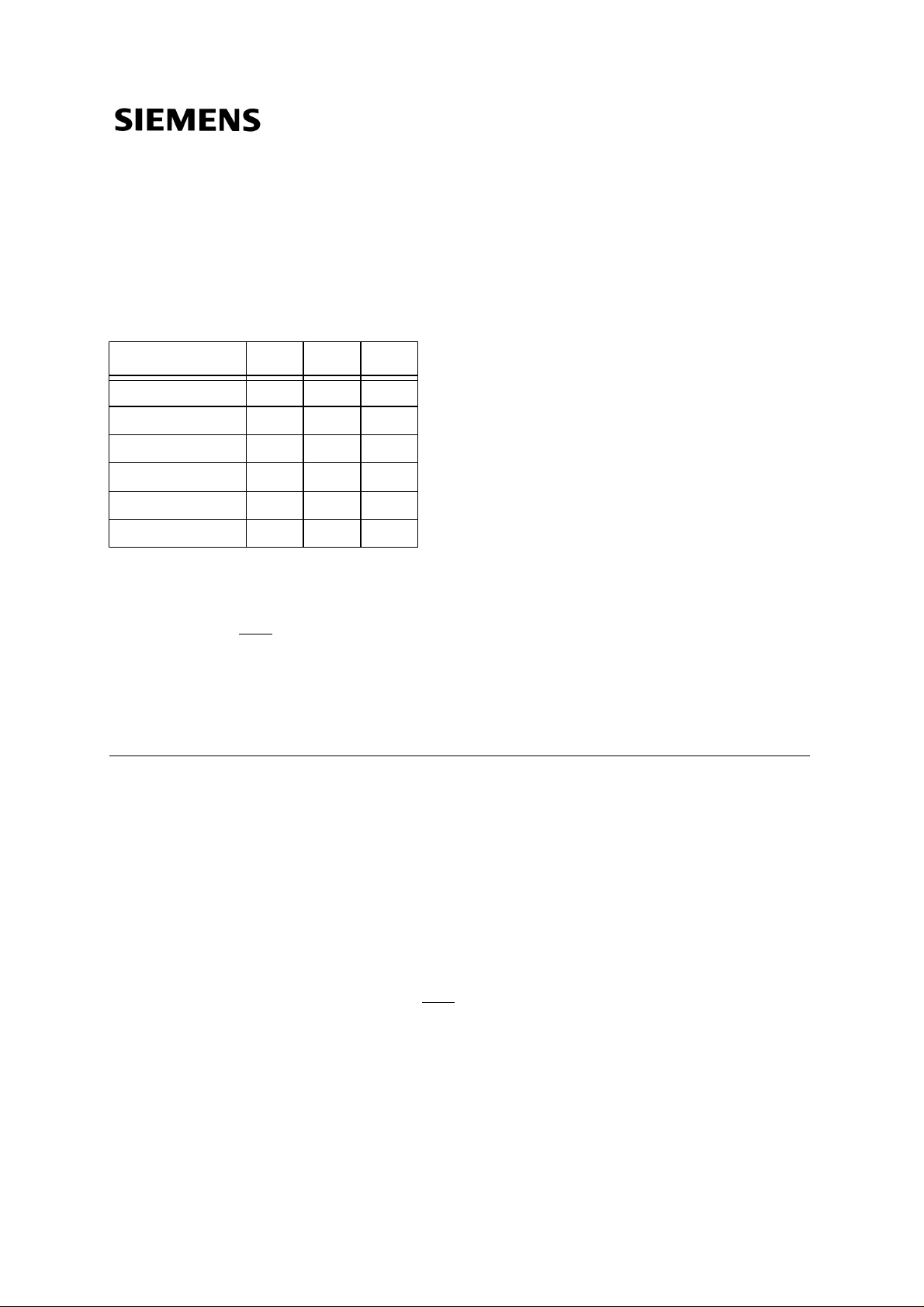
• High Performance:
-6 -7 Units
fCKmax @ CL=3 166 143 MHz
tCK3 6 7 ns
tAC3 5 5.5 ns
fCKmax @ CL=2 125 115 MHz
tCK2 8 9 ns
tAC2 6 6 ns
• Fully Synchronous to Positive Clock Edge
• 0 to 70 °C operating temperature
• Dual Banks controlled by A11 ( Bank Select)
• Programmable CAS Latency : 2, 3
• Programmable Wrap Sequence : Sequential
or Interleave
• Programmable Burst Length: 1, 2, 4, 8
• full page(optional) for sequencial wrap
around
• Multiple Burst Read with Single Write
Operation
• Automatic and Controlled Precharge
Command
• Data Mask for Read / Write control
• Dual Data Mask for byte control ( x16)
• Auto Refresh (CBR) and Self Refresh
• Suspend Mode and Power Down Mode
• 4096 refresh cycles / 64 ms
• Latency 2 @ 125 MHz
• Latency 3 @ 166 MHz
• Random Column Address every CLK
( 1-N Rule)
• Single 3.3V +/- 0.3V Power Supply
• LVTTL Interface
• Plastic Packages:
P-TSOPII-50 400mil width ( x16 )
The HYB39S16160CT-6/-7 are high speed dual bank Synchronous DRAM’s based on SIEMENS
0.25µm process and organized as 2 banks x 512kbit x 16. These synchronous devices achieve high
speed data transfer rates up to 166 MHz by employing a chip architecture that prefetches multiple
bits and then synchronizes the output data to a system clock. The chip is fabricated with SIEMENS’
advanced 16MBit DRAM process technology.
The device is designed to comply with all JEDEC s tandards set for s ynchronous D RAM products,
both electrically and mechani cally. All of the control, addr ess, data input and outpu t circuits are
synchronized with the positive edge of an externally supplied clock.
Operating the two memory banks in an interleaved fashion allows random access operation to occur
at higher rate than is possible with standard DRAMs. A sequential and gapless data rate of up to 166
MHz is possible depending on burst length, CAS
latency and speed grade of the device.
Auto Refresh (CBR) and Self Refresh operation are supported. These devices operate with a single
3.3V +/- 0.3V power supply and are available in TSOPII packages.
These Synchronous DRAM devices are av ailable with LV-TTL interfaces.
Semiconductor Group 1 10.98
HYB39S16160CT-6/-7
16MBit Synchronous DRAM
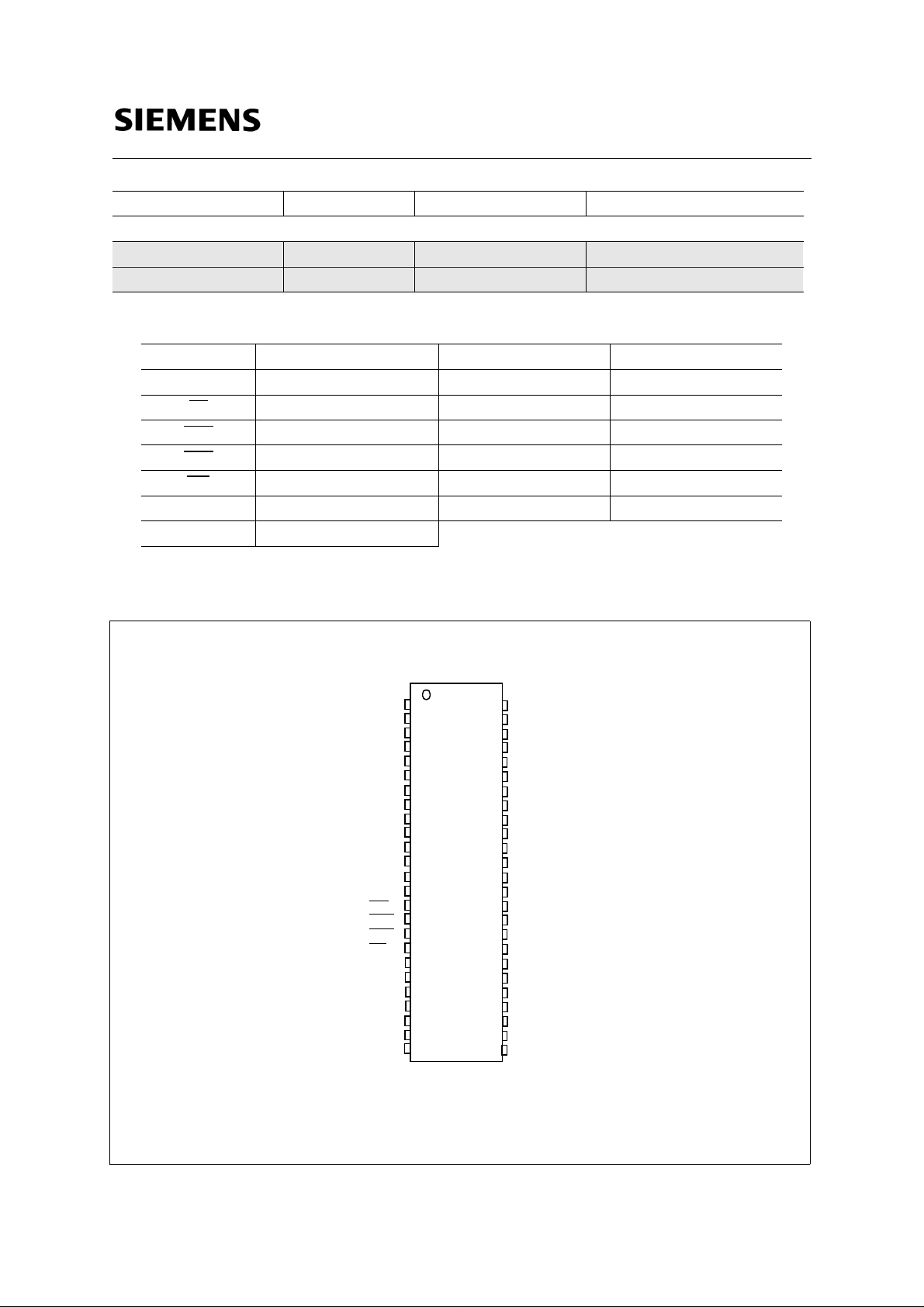
Ordering Information
Type Ordering Code Package Description
LVTTL-version:
HYB 39S16160CT-6 P-TSOPII-50 (400mil) 166MHz 2B x 512k x 16 SDRAM
HYB 39S16160CT-7 P-TSOPII-50 (400mil) 143MHz 2B x 512k x 16 SDRAM
Pin Description and Pinouts:
CLK Clock Input DQ Data Input /Output
CKE Clock Enable LDQM, UDQM Data Mask
CS
RAS
CAS
WE
A0-A10 Address Inputs NC not connected
A11 (BS) Bank Select
Chip Select Vdd Pow e r (+3.3V )
Row Address Strobe Vss Ground
Column Address Strobe Vddq Power for DQ’s (+ 3.3V)
Write Enable Vssq Ground for DQ’s
Pin-Out
Vdd
DQ0
DQ1
Vssq
DQ2
DQ3
Vddq
DQ4
DQ5
Vssq
DQ6
DQ7
Vddq
LDQM
WE
CAS
RAS
CS
A11
A10
A0
A1
A2
A3
Vdd
1
2
3
4
5
6
7
8
9
10
11
12
13
14
15
16
17
18
19
20
21
22
23
24
25
44
43
42
41
40
39
38
37
36
35
34
33
32
31
30
29
28
27
26
50
49
48
47
46
45
Vss
DQ15
DQ14
Vssq
DQ13
DQ12
Vddq
DQ11
DQ10
Vssq
DQ9
DQ8
Vddq
NC
UDQM
CLK
CKE
NC
A9
A8
A7
A6
A5
A4
Vss
Semiconductor Group 2
16MBit Synchronous DRAM
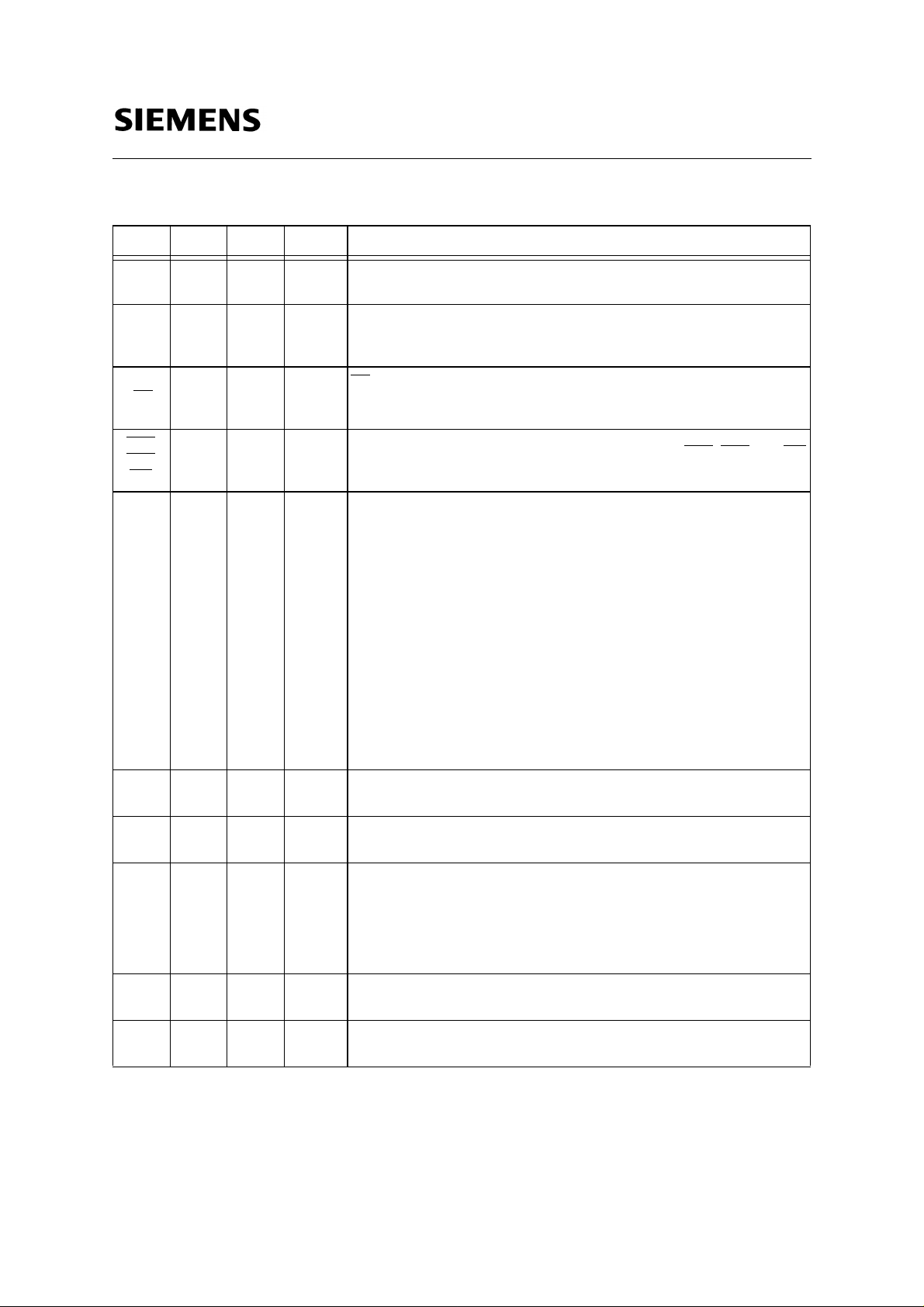
Signal Pin Description
Pin Type Signal Polarity Function
HYB39S16160CT-6/-7
CLK Input Pulse
CKE Input Level
CS
RAS
CAS
A0 -
A10
Input Pulse
,
WEInput Pulse
Input L evel
Positive
Edge
Active
High
Active
Low
Active
Low
—
The system clock input. All of the SDRAM inputs are sampled on the rising
edge of the clock.
Activates the CLK signal when high and deactivates the CLK signal when
low, thereby inititiates either the Power Down mode, Suspend mode or the
Self Refresh mode.
CS
enables the command decoder when low and disables the command
decoder when high. When the command decoder is disabled, new
commands are ignored but previous operations continue.
When sampled at the positive rising edge of the clock, CAS
define the command to be executed by the SDRAM.
During a Bank Activate command cycle, A0-A10 defines the row address
(RA0-RA10) when sampled at the rising clock edge.
During a Read or Write command cycle, A0-A9 defines the column
address (CA0-CAn) when sampled at the rising clock edge.CAn depends
from the SDRAM organisation.
1M x 16 SDRAM CAn = CA7
In addition to the column address, A10 is used to invoke autoprecharge
operation at the end of the burst read or write cycle. If A10 is high,
autoprecharge is selected and A11 defines the bank to be precharged
(low=bank A, high=bank B). If A10 is low, autoprecharge is disabled.
During a Precharge command cycle, A10 is used in conjunction with A11
to control which bank(s) to precharge. If A10 is high, both bank A and bank
B will be precharged regardless of the state of A11. If A10 is low, then A11
is used to define which bank to precharge.
, RAS, and WE
A11
(BS)
DQx
LDQM,
UDQM
VDD,
VSS
VDDQ
VSSQ
Input Level
Input
Output
Input Pulse
Supply Power and ground for the input buffers and the core logic.
Supply — —
Level
Active
High
Selects which bank is to be active. A11 low selects bank A and A1 1 high
—
selects bank B.
Data Input/Output pins operate in the same manner as on conventional
—
DRAMs.
The Data Input/Output mask places the DQ buffers in a high impedance
state when sampled high. In Read mode, DQM has a latency of two clock
cycles and controls the output buffers like an output enable. In Write
mode, DQM has a latency of zero and operates as a word mask by
allowing input data to be written if it is low but blocks the write operation if
DQM is high.
Power supply and ground for the output buffers to provide improved noi se
immunity.
Semiconductor Group 3
CKE
CLK
A0
A1
A2
A3
A4
A5
A6
A7
A8
A9
A10
A11 (BS)
CS
RAS
CAS
CKE Buffer
CLK Buffer
Address Buffers (12)
CS Buffer
RAS Buffer
CAS Buffer
Refresh Clock
12
12
Self
Row
Address
Counter
Command Decoder
Row/Column
Predeco de A
11
11
Predecode B
Row/Column
Bank A
Select
Bank B
Select
Row Decoder
Row Decoder
3
Mode Regi s te r
11
Sequential
3
Row Decoder
Row Decoder
16
16
Sequential
Control
Bank A
Control
Bank B
16
16
HYB39S16160CT-6/-7
16MBit Synchronous DRAM
2048 x 512
Memory Bank A
2048 x 256
Memory Bank A
2048
Column Decoder and DQ Gate
Column Deco der and DQ Gate
16
16
Column Decoder and DQ Gate
1024
512
1024
256
Sense Amplifiers
Sense Amplifiers
Sense Amplifiers
Sense Amplifiers
Column Decoder and DQ Gate
Column Decoder and DQ Gate
8
8
8
Data Latches
Data Latches
Data Latches
Data Latches
Data Latches
Data Latches
Column Decoder and DQ Gate
Sense Amplifiers
Sense Amplifiers
8
8
256
16
8
8
Data Input/Output Buffers
DQ0
DQ1
DQ2
DQ3
DQ4
DQ5
DQ6
DQ7
DQ8
DQ9
DQ10
DQ11
DQ12
DQ13
DQ14
DQ15
WE
UDQM
LDQM
WE Buffer
DQM Buffer
DQM Buffer
2048
Memory Bank B
Memory Bank B
2048 x 256
Memory Bank B
2048 x 1024
Memor y Bank B
Row Decoder
Row Dec o d e r
Row Decoder
Row Decoder
2048 x 512
2048 x 1024
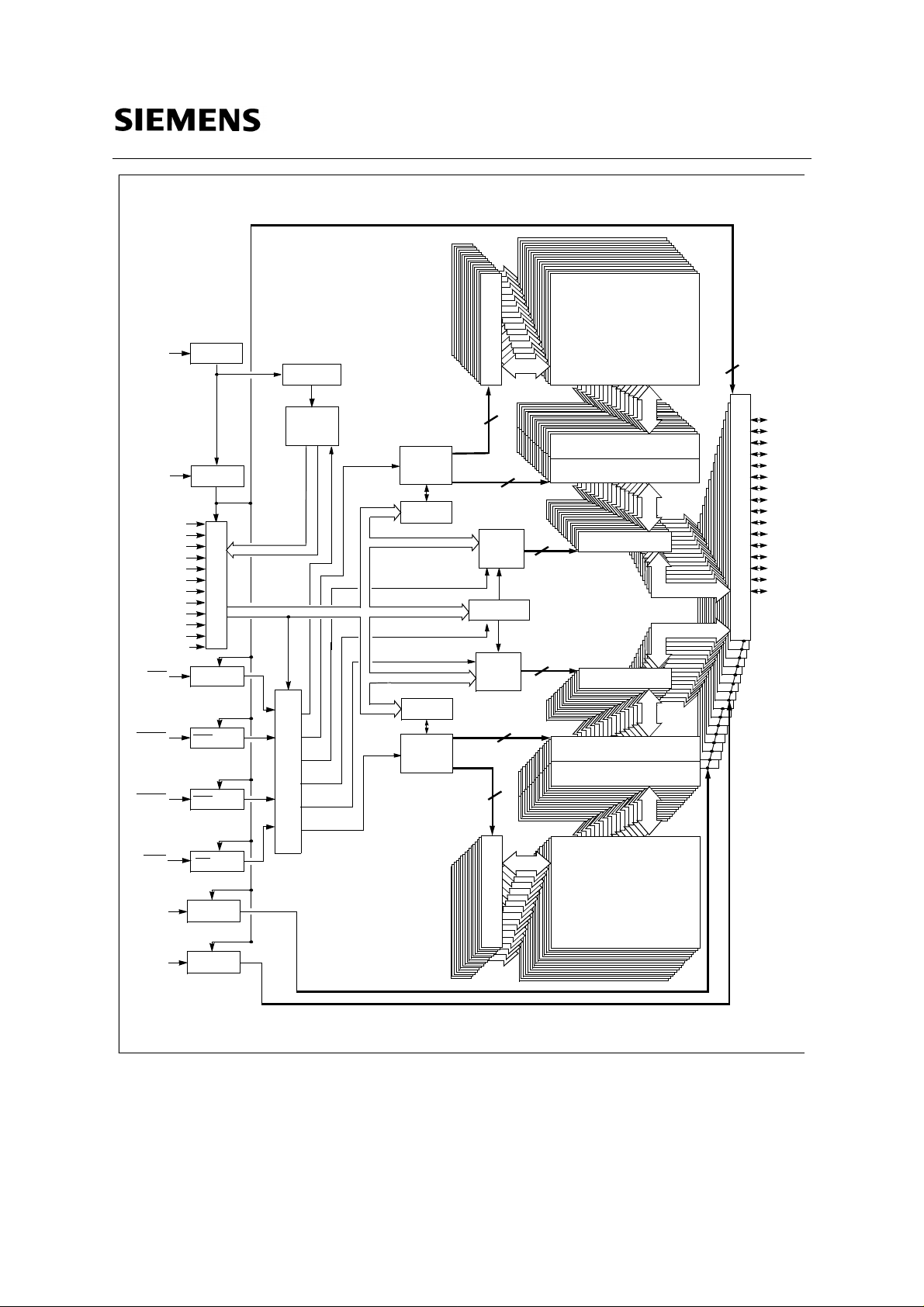
Block Diagram for HYB39S16160CT (2 banks x 512k x 16 SDRAM)
Semiconductor Group 4
Operation Definition
HYB39S16160CT-6/-7
16MBit Synchronous DRAM
All of SDRAM operations are defined by states of control signals CS
, RAS, CAS, WE, and DQM at
the positive edge of the clock. The following list shows the most important operation commands.
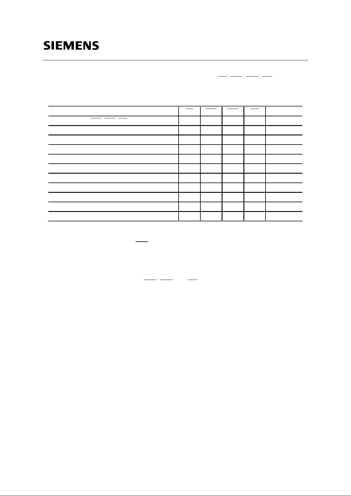
Operation CS RAS CAS WE (L/U)DQM
Standby, Ignore RAS
Row Address Strobe and Activating a Bank L L H H X
Column Address Strobe and Read Command L H L H X
Column Address Strobe and Write Command L H L L X
Precharge Command L L H L X
Burst Stop Command L H H L X
Self Refresh Entry L L L H X
Mode Register Set Command L L L L X
Write Enable/Output Enable X X X X L
Write Inhibit/Output Disable X X X X H
No Operation (NOP) L H H H X
, CAS, WE and Address H X X X X
Mode Register
For application flexibility, a CAS
latency, a burst length, and a burst sequence can be
programmed in the SDR AM mode register. The mode set operation must be done before any
activate command after the initial power up. Any content of the mode register can be altered by reexecuting the mode set command. Both banks must be in precharged state and CKE must be high
at least one clock before the mode set operation. After the mode register is set, a Standby or NOP
command is required. Low signals of RAS
, CAS, and WE at the positive edge of the clock activate
the mode set operation. Address input data at this timing defines parameters to be set as shown in
the following table.
Semiconductor Group 5
 Loading...