

Siemens BUZ11S2 Datasheet
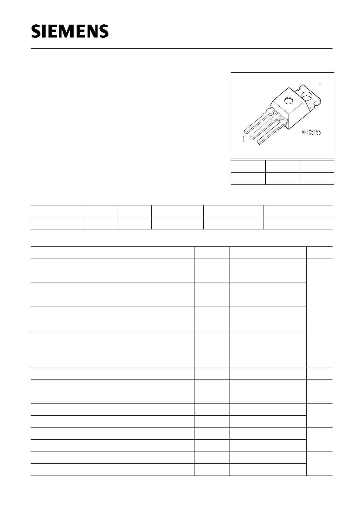
SIPMOS ® Power Transistor
• N channel
• Enhancement mode
• Avalanche-rated
BUZ 11 S2
Not for new design
Pin 1 Pin 2 Pin 3
G D S
Type
BUZ 11 S2 60 V 30 A 0.04
V
DS
I
D
R
DS(on)
Ω
Package Ordering Code
TO-220 AB C67078-S1301-A5
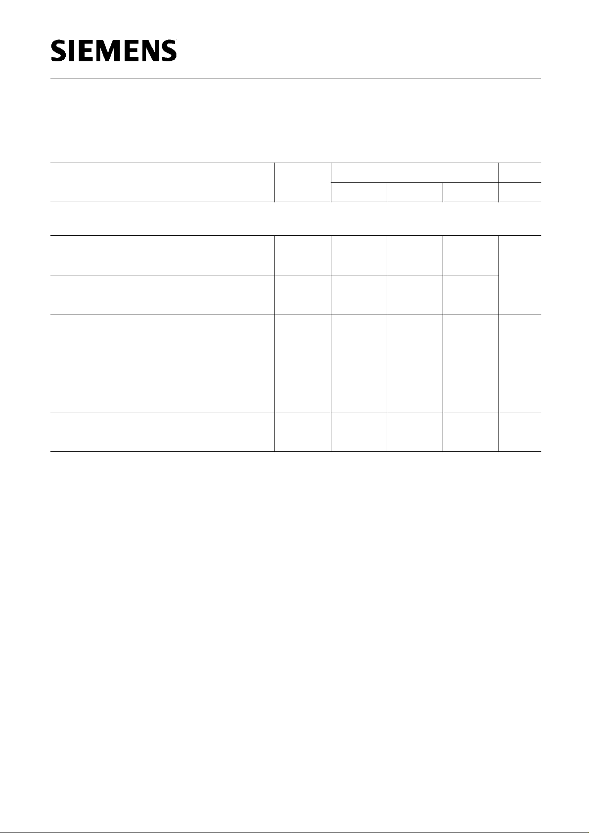
Maximum Ratings
Parameter Symbol Values Unit
Continuous drain current
T
= 29 °C
C
Pulsed drain current
T
= 25 °C
C
Avalanche current,limited by
T
jmax
Avalanche energy,periodic limited by
Avalanche energy, single pulse
I
= 30 A,
D
L
= 15.6 µH,
V
DD
T
= 25 V,
= 25 °C
j
R
GS
= 25
Ω
Gate source voltage
Power dissipation
T
= 25 °C
C
Operating temperature
T
jmax
I
D
I
Dpuls
I
AR
E
AR
E
AS
V
GS
P
tot
T
j
A
30
120
30
1.9 mJ
14
±
20 V
W
75
-55 ... + 150 °C
Storage temperature
Thermal resistance, chip case
Thermal resistance, chip to ambient
T
R
R
stg
thJC
thJA
-55 ... + 150
≤
1.67 K/W
≤
75
DIN humidity category, DIN 40 040 E
IEC climatic category, DIN IEC 68-1 55 / 150 / 56
Semiconductor Group 1 07/96
BUZ 11 S2
Not for new design
Electrical Characteristics, at
T
= 25°C, unless otherwise specified
j
Parameter Symbol Values Unit
min. typ. max.
Static Characteristics
Drain- source breakdown voltage
V
= 0 V,
GS
I
= 0.25 mA,
D
T
= 25 °C
j
Gate threshold voltage
V
GS
V
=
DS, ID
= 1 mA
Zero gate voltage drain current
V
V
DS
DS
= 60 V,
= 60 V,
V
V
GS
GS
= 0 V,
= 0 V,
T
= 25 °C
j
T
= 125 °C
j
Gate-source leakage current
V
= 20 V,
GS
V
DS
= 0 V
Drain-Source on-resistance
V
= 10 V,
GS
I
= 19 A
D
V
(BR)DSS
V
GS(th)
I
DSS
I
GSS
R
DS(on)
60 - -
2.1 3 4
-
-
0.1
10
1
100
- 10 100
- 0.03 0.04
V
µA
nA
Ω
Semiconductor Group 2 07/96
BUZ 11 S2
Not for new design
Electrical Characteristics, at
T
= 25°C, unless otherwise specified
j
Parameter Symbol Values Unit
min. typ. max.
Dynamic Characteristics
Transconductance
≥
V
2
DS
I
*
D * RDS(on)max, ID
= 19 A
Input capacitance
V
= 0 V,
GS
V
= 25 V, f = 1 MHz
DS
Output capacitance
V
= 0 V,
GS
V
= 25 V, f = 1 MHz
DS
Reverse transfer capacitance
V
= 0 V,
GS
V
= 25 V, f = 1 MHz
DS
Turn-on delay time
V
R
DD
GS
= 30 V,
= 50
Ω
V
GS
= 10 V,
I
= 3 A
D
g
fs
C
iss
C
oss
C
rss
t
d(on)
S
10 17 -
pF
- 1000 1350
- 450 680
- 165 250
ns
- 15 25
Rise time
V
R
DD
GS
= 30 V,
= 50
Ω
V
GS
= 10 V,
Turn-off delay time
V
R
DD
GS
= 30 V,
= 50 Ω
V
GS
= 10 V,
Fall time
V
R
DD
GS
= 30 V,
= 50 Ω
V
GS
= 10 V,
I
= 3 A
D
I
= 3 A
D
I
= 3 A
D
t
r
t
d(off)
t
f
- 55 85
- 120 160
- 80 110
Semiconductor Group 3 07/96
 Loading...