

Siemens BUZ102SL-4 Datasheet
®
SIPMOS
Power Transistor
• Quad-channel
• Enhancement mode
• Logic level
• Avalanche-rated
v/dt
• d
rated
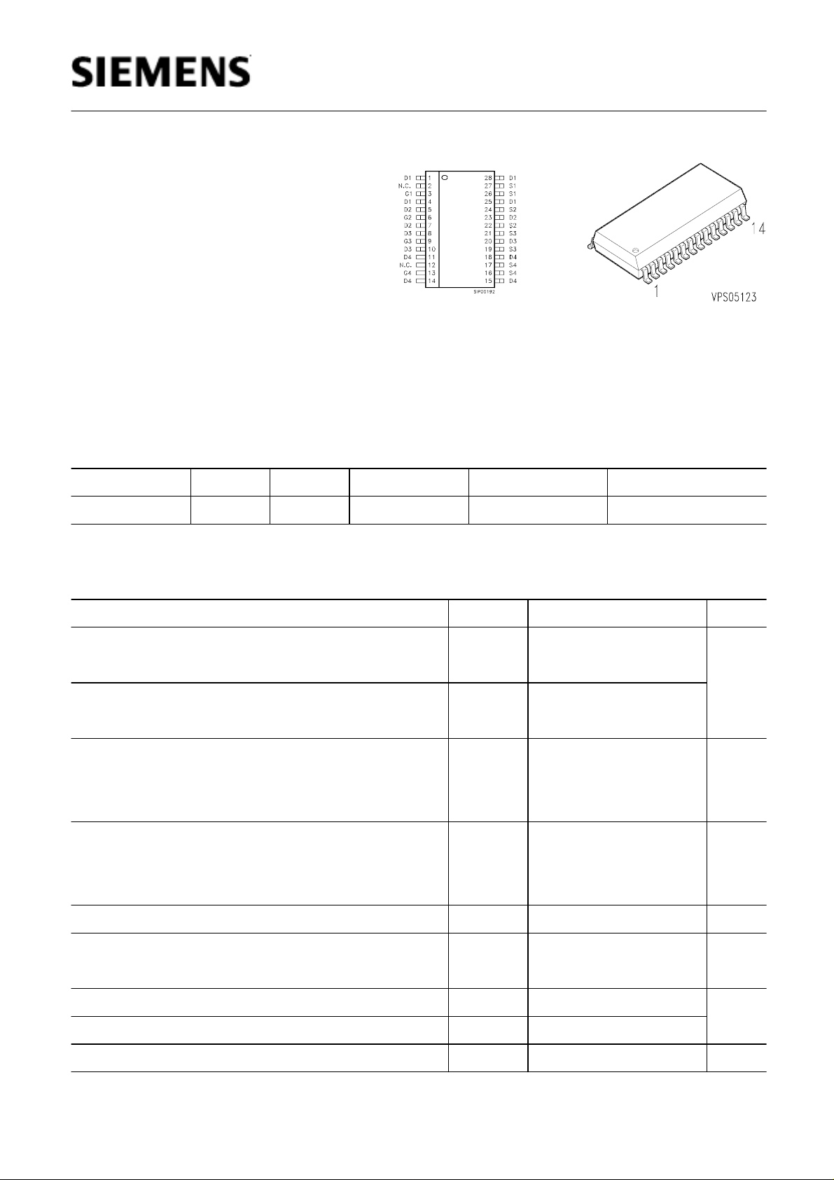
BUZ 102SL-4
Preliminary data
Type
V
DS
BUZ 102SL-4 55 V 6.2 A 0.033
I
D
R
DS(on)
Ω
Package Ordering Code
P-DSO-28 C67078-S. . . .- . .
Maximum Ratings
Parameter
Continuous drain current
= 25 °C
T
A
Pulsed drain current
= 25 °C
T
A
one channel active
one channel active
Avalanche energy, single pulse
I
= 6.2 A,
D
L
= 12.7 mH,
Reverse diode dv/d
= 6.2 A,
I
S
T
= 175 °C
jmax
V
V
DD
T
DS
= 25 V,
= 25 °C
j
t
= 40 V, d
R
= 25
GS
i
/dt = 200 A/µs
F
Gate source voltage
Power dissipation
T
= 25 °C
A
,one channel active
Operating temperature
Storage temperature
Ω
Symbol Values Unit
I
D
6.2
I
Dpuls
24.8
E
AS
245
v/dt
d
6
±
V
P
GS
tot
14
2.4
T
j
T
stg
-55 ... + 175 °C
-55 ... + 175
IEC climatic category, DIN IEC 68-1 55 / 175 / 56
A
mJ
kV/µs
V
W
Semiconductor Group
1 23/Oct/1997
Thermal Characteristics
BUZ 102SL-4
Preliminary data
Parameter
Symbol Values Unit
min. typ. max.
Thermal resistance, junction - soldering point
Thermal resistance, junction - ambient
1) Device on 50mm*50mm*1.5mm epoxy PCB FR4 with 6 cm2 (one layer,70µm thick) copper area for
Drain connection. PCB is vertical without blown air.
2) one channel active
Electrical Characteristics,
= 25°C, unless otherwise specified
at
T
j
2)
1)
R
R
thJS
thJA
- - tbd K/W
- - 62.5
Parameter
Static Characteristics
Drain- source breakdown voltage
V
GS
= 0 V,
= 0.25 mA,
I
D
= 25 °C
T
j
Gate threshold voltage
V
GS
=
V
DS, ID
= 90 µA
Zero gate voltage drain current
V
V
V
DS
DS
DS
= 55 V,
= 55 V,
= 55 V,
V
V
V
= 0 V,
GS
= 0 V,
GS
= 0 V,
GS
= -40 °C
T
j
= 25 °C
T
j
= 150 °C
T
j
Gate-source leakage current
V
GS
= 20 V,
V
DS
= 0 V
Drain-Source on-resistance
V
GS
= 5 V,
= 6.2 A
I
D
Symbol Values Unit
min. typ. max.
V
(BR)DSS
V
55 - -
V
GS(th)
1.2 1.6 2
I
DSS
I
GSS
-
-
-
-
0.1
-
0.1
1
100
µA
nA
- 10 100
R
DS(on)
Ω
- 0.025 0.033
Semiconductor Group
2 23/Oct/1997
Preliminary data
BUZ 102SL-4
Electrical Characteristics,
Parameter
Dynamic Characteristics
Transconductance
≥
2
V
DS
I
*
D * RDS(on)max, ID
Input capacitance
V
GS
= 0 V,
= 25 V, f = 1 MHz
V
DS
Output capacitance
V
GS
= 0 V,
= 25 V, f = 1 MHz
V
DS
Reverse transfer capacitance
V
GS
= 0 V,
= 25 V, f = 1 MHz
V
DS
Turn-on delay time
V
R
DD
G
= 30 V,
= 3.6
Ω
V
= 5 V,
GS
= 6.2 A
I
D
Rise time
V
R
DD
G
= 30 V,
= 3.6
Ω
V
= 5 V,
GS
= 6.2 A
I
D
Turn-off delay time
V
R
DD
G
= 30 V,
= 3.6
Ω
V
= 5 V,
GS
= 6.2 A
I
D
Fall time
V
R
DD
G
= 30 V,
= 3.6
Ω
V
= 5 V,
GS
= 6.2 A
I
D
Gate charge at threshold
V
DD
= 40 V,
≥ 0.1 A,
I
D
V
GS
Gate charge at 5.0 V
V
DD
= 40 V,
= 6.2 A,
I
D
V
GS
Gate charge total
V
DD
= 40 V,
= 6.2 A,
I
D
V
GS
Gate plateau voltage
V
DD
= 40 V,
= 6.2 A
I
D
= 25°C, unless otherwise specified
at
T
j
Symbol Values Unit
min. typ. max.
g
fs
= 6.2 A
C
iss
5 11 -
- 1380 1730
C
oss
- 410 515
C
rss
- 230 290
t
d(on)
- 25 40
t
r
- 37 55
t
d(off)
- 75 115
t
f
- 37 55
Q
g(th)
=0 to 1 V
=0 to 5 V
=0 to 10 V
Q
g(5)
Q
g(total)
V
(plateau)
- 2.5 3.75
- 37 55
- 62 93
- 2.6 -
S
pF
ns
nC
V
Semiconductor Group
3 23/Oct/1997
 Loading...