

Page 1
现货库存、技术资料、百科信息、热点资讯,精彩尽在鼎好!
PROFET® BTS 728 L2
Smart High-Side Power Switch
Two Channels: 2 x 60mΩ
Status Feedback
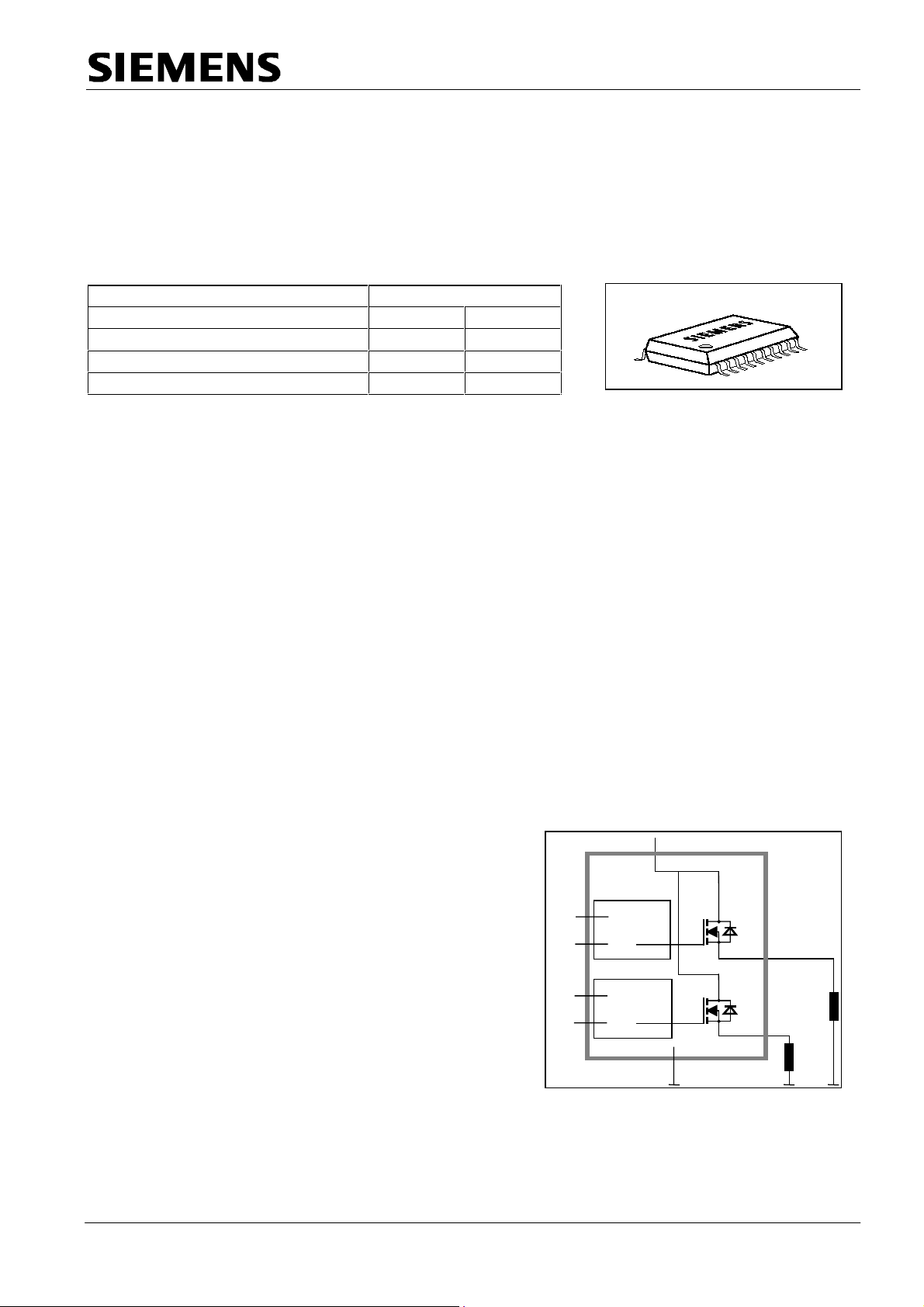
Product Summary Package
Operating Voltage V
bb(on)
4.75...41V
P-DSO-20-9
Active channels one two parallel
On-state Resistance R
Nominal load current I
Current limitation I
ON
L(NOM)
L(SCr)
Ω
60m
4.0A 6.0A
17A 17A
30m
Ω
General Description
•
N channel vertical power MOSFET with charge pump, ground referenced CMOS compatible input and
diagnostic feedback, monolithically integrated in Smart SIPMOS
•
Fully protected by embedded protection functions
technology.
Applications
•
µC compatible high-side power switch with diagnostic feedback for 5V, 12V and 24V grounded loads
•
All types of resistive, inductive and capacitve loads
•
Most suitable for loads with high inrush currents, so as lamps
•
Replaces electromechanical relays, fuses and discrete circuits
Basic Functions
•
Very low standby current
•
CMOS compatible input
•
Improved electromagnetic compatibility (EMC)
•
Fast demagnetization of inductive loads
•
Stable behaviour at undervoltage
•
Wide operating voltage range
•
Logic ground independent from load ground
Protection Functions
•
Short circuit protection
•
Overload protection
•
Current limitation
•
Thermal shutdown
•
Overvoltage protection (including load dump) with external
resistor
•
Reverse battery protection with external resistor
•
Loss of ground and loss of V
protection
bb
• Electrostatic discharge protection (ESD)
Diagnostic Function
• Diagnostic feedback with open drain output
• Open load detection in ON-state
Block Diagram
Vbb
IN1
ST1
IN2
ST2
Logic
Channel
1
Logic
Channel
2
PROFET
GND
OUT 1
Load 1
OUT 2
Load 2
• Feedback of thermal shutdown in ON-state
Semiconductor Group Page 1 of 14 1999-Mar-23
Page 2
Functional diagram
g
y
BTS 728 L2
IN1
ST1
GND1
IN2
ST2
GND2
overvoltage
protection
internal
e suppl
volta
ESD
gate
control
+
charge
logic
pump
temperature
sensor
Open load
detection
Channel 1
Control and protection circuit
of
channel 2
current limit
clamp for
inductive load
VBB
OUT1
LOAD
OUT2
PROFET
Pin Definitions and Functions
Pin Symbol Function
1,10,
11,12,
15,16,
19,20
3IN1
7 IN2 logic high signal
17,18 OUT1
13,14 OUT2 of channel 1,2. Design the wiring for the max.
4ST1
8 ST2 open drain, low on failure
2 GND1
6 GND2
5,9 N.C.
V
bb
Positive power supply voltage. Design the
wiring for the simultaneous max. short circuit
currents from channel 1 to 2 and also for low
thermal resistance
Input 1,2, activates channel 1,2 in case of
Output 1,2, protected high-side power output
short circuit current
Diagnostic feedback 1,2 of channel 1,2,
Ground 1 of chip 1 (channel 1)
Ground 2 of chip 2 (channel 2)
Not Connected
Pin configuration
(top view)
V
1 • 20 V
bb
GND1 2 19 V
IN1 3 18 OUT1
ST1 4 17 OUT1
N.C. 5 16 V
GND2 6 15 V
IN2 7 14 OUT2
ST2 8 13 OUT2
N.C. 9 12 V
Vbb10 11 V
bb
bb
bb
bb
bb
bb
Semiconductor Group Page 2 1999-Mar-23
Page 3
BTS 728 L2
Maximum Ratings at
T
= 25°C unless otherwise specified
j
Parameter Symbol Values Unit
Supply voltage (overvoltage protection see page 4)
Supply voltage for full short circuit protection
T
= -40 ...+150°C
j,start
Load current (Short-circuit current, see page 5)
Load dump protection1)
2)
R
= 2 Ω,
I
t
= 200 ms; IN = low or high,
d
each channel loaded with
V
LoadDump
R
=
= 8.0 Ω,
L
V
+
V
,
V
s
= 13.5 V
A
A
Operating temperature range
Storage temperature range
Power dissipation (DC)
(all channels active)
4)
T
= 25°C:
a
T
= 85°C:
a
V
bb
V
bb
I
L
V
Load dump
T
j
T
stg
P
tot
43 V
24 V
self-limited A
3
)
-40 ...+150
60 V
°C
-55 ...+150
3.7
W
1.9
Maximal switchable inductance, single pulse
V
I
I
bb
L
L
= 12V,
= 4.0 A,
= 6.0 A,
T
= 150°C4),
j,start
E
= 220 mJ, 0 Ω one channel:
AS
E
= 540 mJ, 0 Ω two parallel channels:
AS
Z
L
19.9
mH
22.3
see diagrams on page 9
Electrostatic discharge capability (ESD) IN:
(Human Body Model) ST:
out to all other pins shorted:
V
ESD
1.0
4.0
8.0
kV
acc. MIL-STD883D, method 3015.7 and ESD assn. std. S5.1-1993
R=1.5kΩ; C=100pF
Input voltage (DC)
Current through input pin (DC)
Current through status pin (DC)
V
I
I
IN
ST
IN
-10 ... +16 V
±2.0
mA
±5.0
see internal circuit diagram page 8
Thermal Characteristics
Parameter and Conditions Symbol Values Unit
min typ Max
Thermal resistance
junction - soldering point
junction - ambient
1)
Supply voltages higher than V
resistor for the GND connection is recommended.
2)
R
= internal resistance of the load dump test pulse generator
I
3)
V
Load dump
4)
Device on 50mm*50mm*1.5mm epoxy PCB FR4 with 6cm
connection. PCB is vertical without blown air. See page 14
5)
Soldering point: upper side of solder edge of device pin 15. See page 14
is setup without the DUT connected to the generator per ISO 7637-1 and DIN 40839
4)
Semiconductor Group Page 3 1999-Mar-23
4),5)
each channel:
one channel active:
all channels active:
require an external current limit for the GND and status pins (a 150Ω
bb(AZ)
R
thjs
R
thja
2
(one layer, 70µm thick) copper area for V
-- -- 13.5
--
--
41
34
K/W
--
--
bb
Page 4
BTS 728 L2
T
j
Electrical Characteristics
Parameter and Conditions, each of the two channels Symbol Values Unit
at Tj = -40...+150°C,
Load Switching Capabilities and Characteristics
V
= 12 V unless otherwise specified
bb
min typ Max
On-state resistance (Vbb to OUT); I
each channel,
two parallel channels,
see diagram, page 10
= 2 A, Vbb ≥ 7V
L
T
= 25°C:
j
T
= 150°C:
j
= 25°C:
Nominal load current one channel active:
two parallel channels active:
6)
Device on PCB
,
T
a
= 85°C,
T
≤ 150°C
j
Output current while GND disconnected or pulled up;
V
= 30 V,
bb
see diagram page 8; (not tested specified by design)
Turn-on time7) IN to 90%
Turn-off time IN to 10%
R
= 12 Ω
L
Slew rate on
10 to 30%
Slew rate off
70 to 40%
V
= 0,
IN
V
OUT
V
OUT
7)
V
,
R
,
R
= 12 Ω:
L
= 12 Ω:
L
V
OUT
7)
OUT
:
:
R
I
I
t
t
dV/dt
-dV/dt
ON
L(NOM)
L(GNDhigh)
on
off
on
off
--
3.6
5.5
50
100
25
4.0
6.0
60
120
30
mΩ
-- A
-- -- 2 mA
30
30
100
100
200
200
µs
0.1 -- 1 V/µs
0.1 -- 1 V/µs
Operating Parameters
Operating voltage Tj=-40
Tj=25...150°C:
10)
8)
T
,
V
= 5V,
IN
T
=-40°C:
j
T
=25...150°C:
j
=-40°C...25°C:
j
T
=150°C:
j
I
)
bb(off)
, one channel on:
Overvoltage protection
I
= 40 mA
bb
Standby current
V
= 0; see diagram page 10
IN
)
9
Leakage output current (included in
V
IN = 0
Operating current
I
=
I
+
GND
GND1
I
GND2
two channels on:
6)
Device on 50mm*50mm*1.5mm epoxy PCB FR4 with 6cm
connection. PCB is vertical without blown air. See page 14
7)
See timing diagram on page 11.
8)
Supply voltages higher than V
resistor for the GND connection is recommended). See also
circuit diagram on page 8.
9)
Measured with load; for the whole device; all channels off
10)
Add
I
, if
I
ST
> 0
ST
require an external current limit for the GND and status pins (a 150Ω
bb(AZ)
V
bb(on)
V
bb(AZ)
I
bb(off)
I
L(off)
I
GND
2
(one layer, 70µm thick) copper area for V
V
in table of protection functions and
ON(CL)
4.75 --
--
41
43
--
--
--
47
10
--
41
43
52
18
50
-- 1 10 µA
--
--
0.8
1.6
1.5
3.0
V
--
V
µA
mA
bb
Semiconductor Group Page 4 1999-Mar-23
Page 5
BTS 728 L2
Parameter and Conditions, each of the two channels Symbol Values Unit
at Tj = -40...+150°C,
Protection Functions
Current limit, (see timing diagrams, page 12)
Repetitive short circuit current limit,
T
=
T
each channel
j
jt
(see timing diagrams, page 12)
Initial short circuit shutdown time
Output clamp (inductive load switch off)
at V
ON(CL)
= Vbb - V
Thermal overload trip temperature
Thermal hysteresis
V
= 12 V unless otherwise specified
bb
T
=+150°C:
T
j
two parallel channels
T
j,start
(see timing diagrams on page 12)
11)
,
I
OUT
= 40 mA
L
T
=25°C...150°C:
T
j
=-40°C:
j
=25°C:
T
j
=25°C:
=-40°C:
j
I
L(lim)
I
L(SCr)
t
off(SC)
V
ON(CL)
T
jt
∆
T
jt
min typ Max
21
17
12
--
--
28
22
16
17
17
36
31
24
A
--
A
--
-- 2.4 -- ms
V
41
43
47
--
--
52
150 -- -- °C
-- 10 -- K
Reverse Battery
Reverse battery voltage
12)
Drain-source diode voltage (V
= - 4.0 A, Tj = +150°C
I
L
out
> V
bb
-
V
bb
)
-
V
ON
-- -- 32 V
-- 600 -- mV
11)
If channels are connected in parallel, output clamp is usually accomplished by the channel with the lowest
V
ON(CL)
12)
Requires a 150 Ω resistor in GND connection. The reverse load current through the intrinsic drain-source
diode has to be limited by the connected load. Power dissipation is higher compared to normal operating
conditions due to the voltage drop across the drain-source diode. The temperature protection is not active
during reverse current operation! Input and Status currents have to be limited (see max. ratings page 3 and
circuit page 8).
Semiconductor Group Page 5 1999-Mar-23
Page 6

BTS 728 L2
Parameter and Conditions, each of the two channels Symbol Values Unit
at Tj = -40...+150°C,
Diagnostic Characteristics
Open load detection current, (on-condition)
V
= 12 V unless otherwise specified
bb
each channel
I
L (OL)1
min typ Max
10 -- 500 mA
Input and Status Feedback
Input resistance
(see circuit page 8)
Input turn-on threshold voltage
Input turn-off threshold voltage
13)
R
V
V
Input threshold hysteresis ∆
Off state input current
On state input current
Delay time for status with open load after switch
V
= 0.4 V:
IN
V
IN
= 5 V:
I
I
t
off; (see diagram on page 13)
Status output (open drain)
Zener limit voltage
ST low voltage
I
= +1.6 mA:
ST
I
= +1.6 mA:
ST
V
V
I
IN(T+)
IN(T-)
V
IN(T)
IN(off)
IN(on)
d(ST OL4)
ST(high)
ST(low)
2.5 3.5 6 kΩ
1.7 -- 3.2 V
1.5 -- -- V
-- 0.5 -- V
1--50µA
20 50 90 µA
100 520 900 µs
5.4
--
6.1
--
0.4
--
V
13)
If ground resistors R
are used, add the voltage drop across these resistors.
GND
Semiconductor Group Page 6 1999-Mar-23
Page 7

BTS 728 L2
Truth Table
Channel 1 Input 1 Output 1 Status 1
Channel 2 Input 2 Output 2 Status 2
level level BTS 728L2
Normal
operation
Open load L
Overtemperature
L = "Low" Level X = don’t care Z = high impedance, potential depends on external circuit
H = "High" Level Status signal valid after the time delay shown in the timing diagrams
Parallel switching of channel 1 and 2 is easily possible by connecting the inputs and outputs in parallel. The
status outputs ST1 and ST2 have to be configured as a ’Wired OR’ function with a single pull-up resistor.
L
H
H
L
H
L
H
Z
H
L
L
H
H
H
L
H
L
Terms
I
bb
V
bb
I
IN1
IN1
3
I
ST1
ST1
V
IN1
4
V
ST1
R
Leadframe (Vbb) is connected to pin 1,10,11,12,15,16,19,20
External R
optional; two resistors R
GND
battery protection up to the max. operating voltage.
GND1
Leadframe
V
bb
PROFET
Chip 1
GND1
2
I
GND1
OUT1
I
L1
17,18
GND1
V
, R
V
ON1
OUT1
GND2
GND2
Leadframe
V
bb
PROFET
Chip 2
GND2
6
I
GND2
OUT2
I
IN2
IN2
7
I
ST2
ST2
V
IN2
8
V
ST2
R
= 150 Ω or a single resistor R
I
V
L2
13,14
GND
ON2
V
OUT2
= 75 Ω for reverse
Semiconductor Group Page 7 1999-Mar-23
Page 8
BTS 728 L2
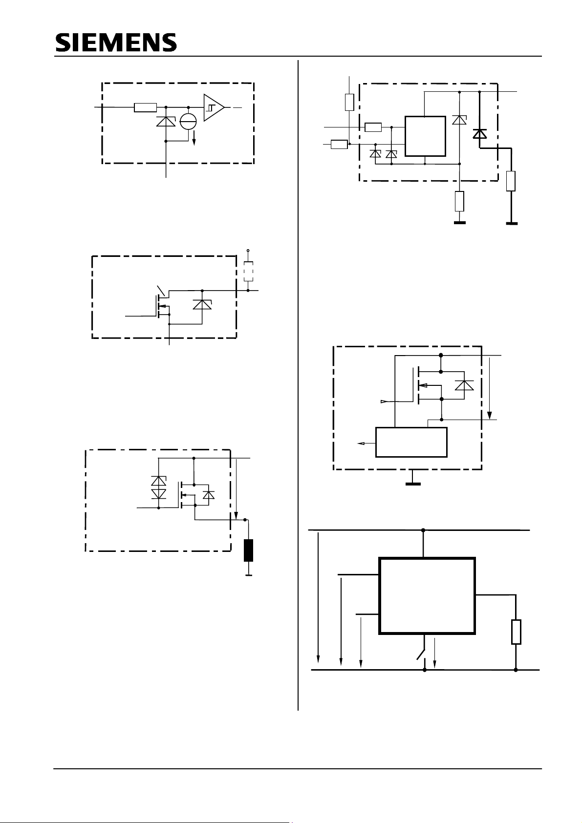
Input circuit (ESD protection), IN1 or IN2
R
IN
I
ESD-ZD
I
GND
I
I
The use of ESD zener diodes as voltage clamp at DC
conditions is not recommended.
Status output, ST1 or ST2
+5V
R
ST(ON)
GND
ESD-Zener diode: 6.1 V typ., max 5.0 mA; R
ESDZD
ST
ST(ON)
< 375 Ω
at 1.6 mA. The use of ESD zener diodes as voltage clamp at
DC conditions is not recommended.
Inductive and overvoltage output clamp,
OUT1 or OUT2
+V
bb
Overvolt. and reverse batt. protection
+ 5V
R
R
ST
V
= 6.1 V typ.,
Z1
R
= 15 kΩ,
ST
ST
R
I
IN
Logic
ST
V
Z1
R
Signal GND
V
= 47 V typ.,
Z2
R
= 3.5 kΩ typ.
I
GND
R
GND
V
Z2
PROFET
GND
In case of reverse battery the load current has to be
limited by the load. Temperature protection is not active
+ V
OUT
R
Load
Load GND
= 150 Ω,
bb
Open-load detection OUT1 or OUT2
ON-state diagnostic
V
Open load, if
Logic
unit
ON
ON
< R
Open load
detection
ON·IL(OL)
; IN high
+ V
OUT
bb
V
ON
V
clamped to
ON
V
ON(CL)
V
Z
= 47 V typ.
Power GND
V
ON
OUT
GND disconnect
V
IN
ST
VbbV
IN
V
ST
Any kind of load. In case of IN = high is
Due to V
> 0, no V
GND
ST
bb
PROFET
GND
V
GND
= low signal available.
OUT
V
OUT
≈
V
-
V
IN(T+)
.
IN
Semiconductor Group Page 8 1999-Mar-23
Page 9

BTS 728 L2
1000
GND disconnect with GND pull up
V
PROFET
>
V
bb
GND
IN
V
-
GND
V
IN(T+)
OUT
device stays off
V
V
bb
V
IN
Any kind of load. If V
Due to V
> 0, no VST = low signal available.
GND
IN
ST
ST
GND
Vbb disconnect with energized inductive
load
high
IN
ST
V
bb
PROFET
GND
OUT
Inductive load switch-off energy
dissipation
E
bb
E
AS
V
E
L
bb
PROFET
GND
1
/
=
·L·I
2
OUT(CL)
OUT
2
L
ON(CL)·iL
|) ln (1+
Ω:
Z
|V
L
L
{
R
L
(t) dt,
I
·R
L
L
OUT(CL)
IN
=
ST
Energy stored in load inductance:
While demagnetizing load inductance, the energy
dissipated in PROFET is
E
= Ebb + EL - ER= ∫ V
AS
with an approximate solution for RL > 0
I
· L
AS
=
L
(V
+ |V
bb
·R
2
L
E
E
Load
E
L
E
R
)
|
V
bb
For inductive load currents up to the limits defined by Z
L
(max. ratings and diagram on page 9) each switch is
protected against loss of Vbb.
Consider at your PCB layout that in the case of Vbb disconnection with energized inductive load all the load current
flows through the GND connection.
Maximum allowable load inductance for
a single switch off (one channel)
L = f (IL );
ZL [mH]
100
10
T
j,start
=
150°C, V
bb
4)
= 12 V, RL = 0 Ω
1
23456789101112
IL [A]
Semiconductor Group Page 9 1999-Mar-23
Page 10

Typ. on-state resistance
RON = f (Vbb,Tj )
[mOhm]
R
ON
125
; I
= 2 A, IN = high
L
BTS 728 L2
100
75
50
25
0
3 5 7 9 30 40
Typ. standby current
I
bb(off)
I
bb(off)
45
= f (Tj )
[µA]
; V
= 9...34 V, IN1,2 = low
bb
Tj = 150°C
25°C
-40°C
Vbb [V]
40
35
30
25
20
15
10
5
0
-50 0 50 100 150 200
Tj [°C]
Semiconductor Group Page 10 1999-Mar-23
Page 11

BTS 728 L2
Timing diagrams
Both channels are symmetric and consequently the diagrams are valid for channel 1 and
channel 2
Figure 1a: Vbb turn on:
IN1
Figure 2b: Switching a lamp:
IN2
V
bb
V
OUT1
V
OUT2
ST1 open drain
ST2 open drain
Figure 2a: Switching a resistive load,
turn-on/off time and slew rate definition:
IN
IN
ST
V
OUT
I
L
t
The initial peak current shoul d be l i m i t ed by the lamp and not by the
current limit of the dev i ce.
Figure 2c: Switching an inductive load
t
V
OUT
90%
10%
I
L
t
on
dV/dto n
IN
ST
dV/dto ff
V
t
off
t
OUT
I
L
I
L(OL)
*) if the time constant of load is too large, open-load-status may
occur
t
Semiconductor Group Page 11 1999-Mar-23
Page 12

BTS 728 L2
Figure 3a: Turn on into short circuit:
shut down by overtemperature, restart by cooling
IN1
I
L1
ST
other channel: normal operation
I
L(lim)
I
L(SCr)
t
off(SC)
Figure 4a: Overtemperature:
T
<
Reset if
T
j
jt
IN
ST
V
OUT
T
J
t
t
Heating up of the chip may require several millisec onds , depending
on external conditions
Figure 3b: Turn on into short circuit:
shut down by overtemperature, restart by cooling
(two parallel switched channels 1 and 2)
IN1/2
I + I
L1 L2
2xI
L(lim)
I
L(SCr)
t
off(SC)
ST1/2
Figure 5a: Open load: detection in ON-state, open
load occurs in on-state
IN
ST
V
I
OUT
L
t
d(ST OL)
normal
open
t
d(ST OL)
normal
t
t
t
ST1 and ST2 have to be configured as a ’Wired OR’ function
ST1/2 with a single pull-up res i stor.
d(ST OL)
= 10 µs typ.
Semiconductor Group Page 12 1999-Mar-23
Page 13

Figure 5b: Open load: turn on/off to open load
IN
t
ST
I
L
d(STOL4)
BTS 728 L2
t
Semiconductor Group Page 13 1999-Mar-23
Page 14
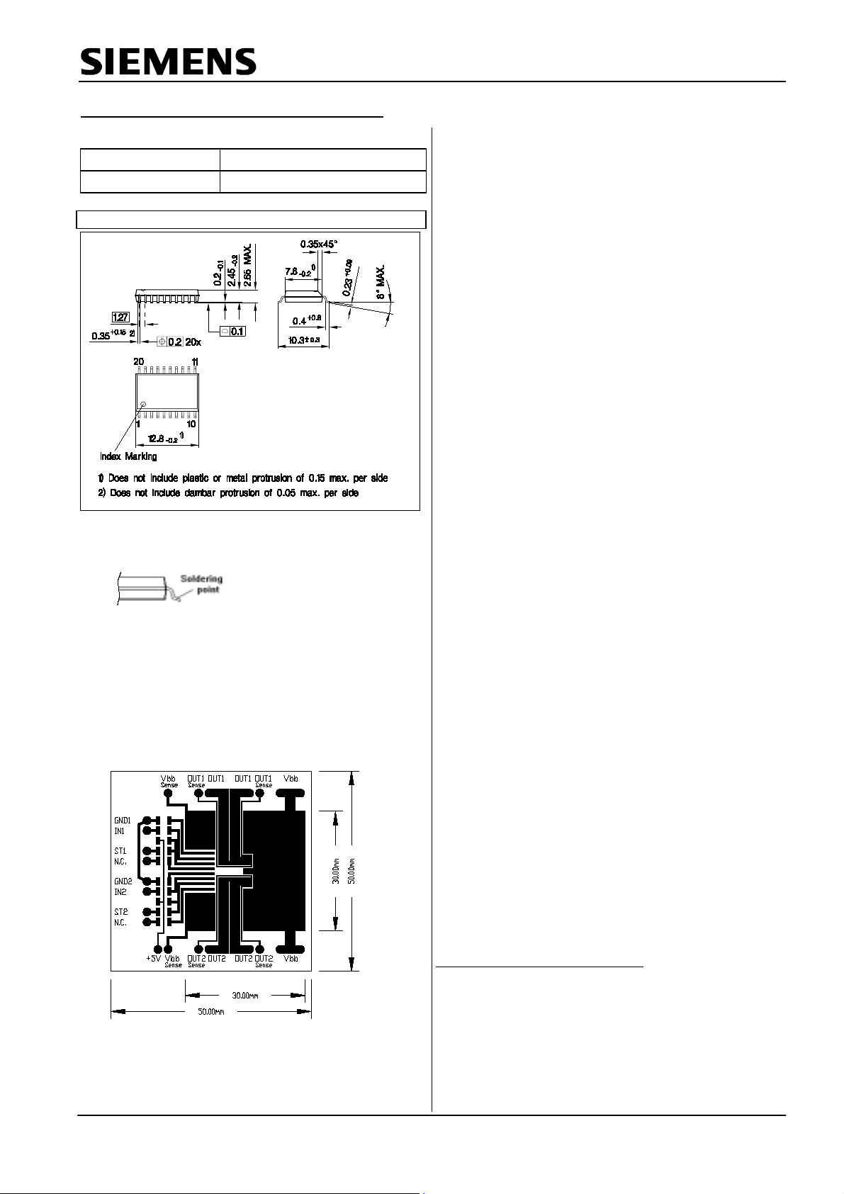
Package and Ordering Code
Pin 15
BTS 728 L2
Standard: P-DSO-20-9
Sales Code BTS 728 L2
Ordering Code Q67060-S7014-A2
All dimensions in millimetres
Definition of soldering point with temperature Ts:
upper side of solder edge of device pin 15.
Published by Siemens AG, Bereich Bauelemente, Vertrieb,
Produkt-Information, Balanstraße 73, D-81541 München
Siemens AG 1999. All Rights Reserved
As far as patents or other rights of third parties are concerned,
liability is only assumed for components per se, not for applicat ions,
processes and circuits implemented within components or assemblies. The information des cribes a type of component and shall not
be considered as warranted characteri stics. The characteristics f or
which SIEMENS grants a warranty will only be specified in the
purchase contract. Terms of delivery and rights to change design
reserved. For questions on tec hnology, delivery and prices please
contact the Offices of Semiconductor Group in Germany or the
Siemens Companies and Representatives woldwide (see address
list). Due to technical requirements components may contain dangerous substances. For inf ormation on the type in question please
contact your nearest Siemens Office, Semiconductor Group.
Siemens AG is an approved CECC m anufacturer.
Packing: Please use the recy cling operators known to you. We c an
also help you - get in touch with your nearest sales office. By
agreement we will take packing material back, if it is sorted. You
must bear the costs of transport. For packing material that is returned to us unsorted or which we are not obliged to ac cept we shal l
have to invoice you for any costs incurred.
Components used in life-support devices or systems must be
14
expressly authorised for such purpose! Critic al component s
the Semiconductor Group of S iemens AG, may only be used in life
)
15
supporting devices or systems
of the Semiconductor Group of S i em ens AG.
with the express writt en approval
)
of
Printed circuit board (FR4, 1.5mm thick, one layer
2
70µm, 6cm
max. power dissipation P
I
L(NOM)
active heatsink area) as a reference for
, nominal load current
and thermal resistance R
tot
thja
14)
A critical component i s a component used in a life-support
device or system whose failure can reasonably be expected to
cause the failure of that l i f e-support device or system, or to
affect its safety or effectiveness of that device or system.
15)
Life support devices or systems are intended (a) to be
implanted in the human body or (b) support and/ or maintain
and sustain and/or protect hum an l i fe. If they fail, it i s
reasonably to assume that the health of the user or other
persons may be endangered.
Semiconductor Group Page 14 1999-Mar-23
 Loading...