

Siemens BSP170P Datasheet
BSP 170 P
DSIDRDS(on)
@ V
GS
jmax
AR
j(max)
AR
jmax
GS
j
stg
Preliminary data
SIPMOS Power Transistor
• P-Channel
• Enhancement mode
• Avalanche rated
• dv/dt rated
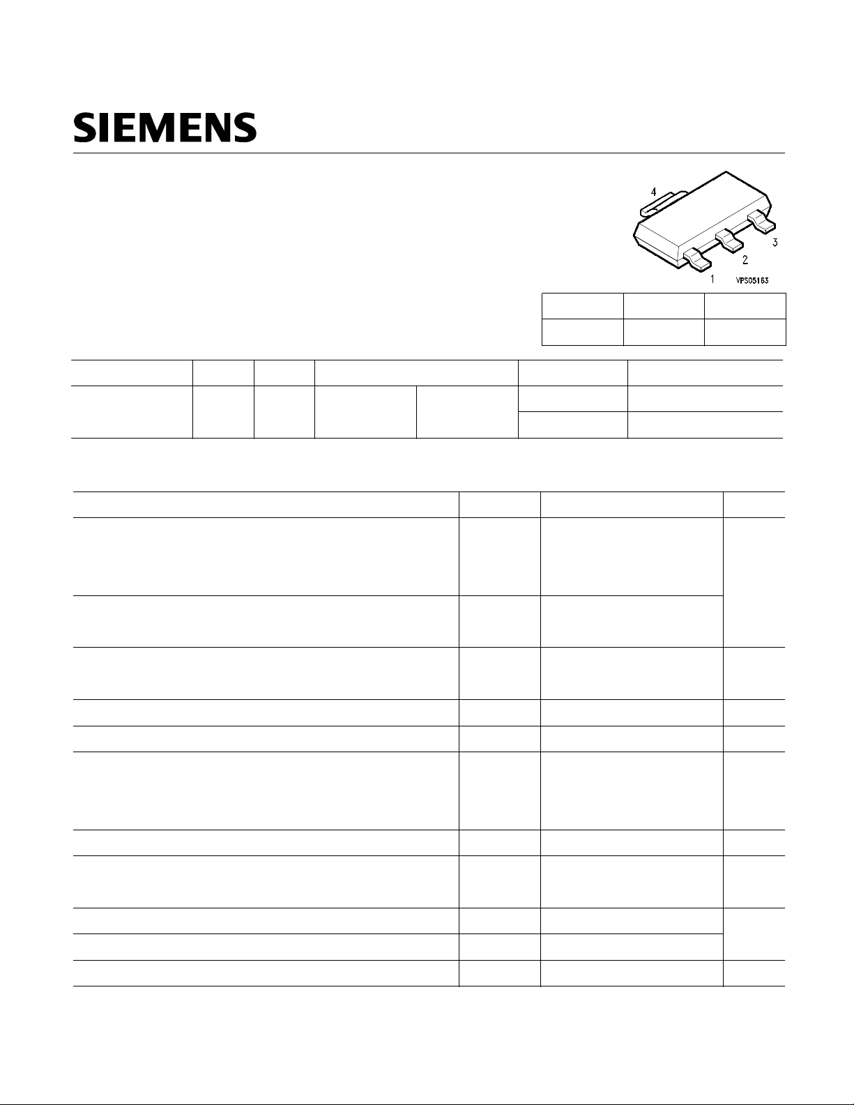
Pin 3Pin 2/4Pin 1
G D S
Type V
Package Ordering Code
BSP 170 P 60 V -1.9 A 0.3 Ω VGS = -10 V SOT-223 Q67041-S4018
-
Maximum Ratings , at Tj = 25°C, unless otherwise specified
Parameter Symbol Value Unit
Continuous drain current
I
D
A
TA = 25 °C
TA = 70 °C
Pulsed drain current
IDpulse -7.6
TA = 25 °C
Avalanche energy, single pulse
E
ID = -1.9 A, VDD = -25 V, RGS = 25 Ω
Avalanche current,periodic limited by T
Avalanche energy,periodic limited by T
Reverse diode dv/dt
IS = -1.9 A, VDD ≤ V
T
= 150 °C
(BR)DSS
, di/dt = 200 A/µs,
I
E
dv/dt 6 kV/µs
Gate source voltage V
Power dissipation
P
TA = 25 °C
Operating temperature °CT
AS
tot
-1.9
-1.5
70 mJ
-1.9 A
0.18 mJ
±20 V
1.8 W
-55 ... +150
-55...+150Storage temperature T
IEC climatic category; DIN IEC 68-1 55/150/56
Semiconductor Group 07 / 19981

BSP 170 P
thJS
Preliminary data
Electrical Characteristics
Parameter ValuesSymbol Unit
at Tj = 25 °C, unless otherwise specified typ. max.min.
Thermal Characteristics
Thermal resistance, junction -soldering point (Pin 4 ) K/W
SMD version, device on PCB:
R
thJA
@ min. footprint
@ 6 cm2 cooling area1)
- - tbdR
-
-
tbd
-
-
70
Static Characteristics
V
(BR)DSS
60 - -Drain- source breakdown voltage
V
VGS = 0 V, ID = -0.25 mA
V
GS(th)
-2.1 -4-3Gate threshold voltage, VGS = VDS
ID = -460 µA
Zero gate voltage drain current
VDS = -60 V, VGS = 0 V, Tj = 25 °C
VDS = -60 V, VGS = 0 V, Tj = 125 °C
VGS = -20 V, VDS = 0 V
VGS = -10 V, ID = -1.9 A
I
DSS
I
GSS
R
DS(on)
-
-
-0.1
-
- -10Gate-source leakage current
-1
-100
µA
nA-100
- 0.175 0.3 ΩDrain-Source on-state resistance
1
Device on 50mm*50mm*1.5mm epoxy PCB FR4 with 6 cm2 (one layer, 70µm thick) copper area for drain
connection. PCB is vertical without blown air.
Semiconductor Group 07 / 19982

BSP 170 P
DS(on)max
Preliminary data
Electrical Characteristics
Parameter Symbol UnitValues
min. typ. max.at Tj = 25 °C, unless otherwise specified
Dynamic Characteristics
VDS≥2*ID*R
, ID = -1.9 A
g
C
fs
iss
1 -2.5Transconductance
- 420 pF335Input capacitance
VGS = 0 V, VDS = -25 V, f = 1 MHz
C
oss
- 105Output capacitance
VGS = 0 V, VDS = -25 V, f = 1 MHz
C
rss
- 65 85Reverse transfer capacitance
VGS = 0 V, VDS = -25 V, f = 1 MHz
d(on)
14-Turn-on delay time
VDD = -30 V, VGS = -10 V, ID = -1.9 A,
135
21
S
nst
RG = 6 Ω
Rise time
VDD = -30 V, VGS = -10 V, ID = -1.9 A,
RG = 6 Ω
Turn-off delay time
VDD = -30 V, VGS = -10 V, ID = -1.9 A,
RG = 6 Ω
Fall time
VDD = -30 V, VGS = -10 V, ID = -1.9 A,
RG = 6 Ω
t
r
d(off)
f
45- 30
190- 125t
- 65t
100
Semiconductor Group 07 / 19983
 Loading...