

Siemens BSP149 Datasheet
SIPMOS Small-Signal Transistor BSP 149
● V
● I
● R
● N channel
● Depletion mode
● High dynamic resistance
● Available grouped in V
Type Ordering
DS
D
DS(on)
200 V
0.48 A
3.5 Ω
Code
GS(th)
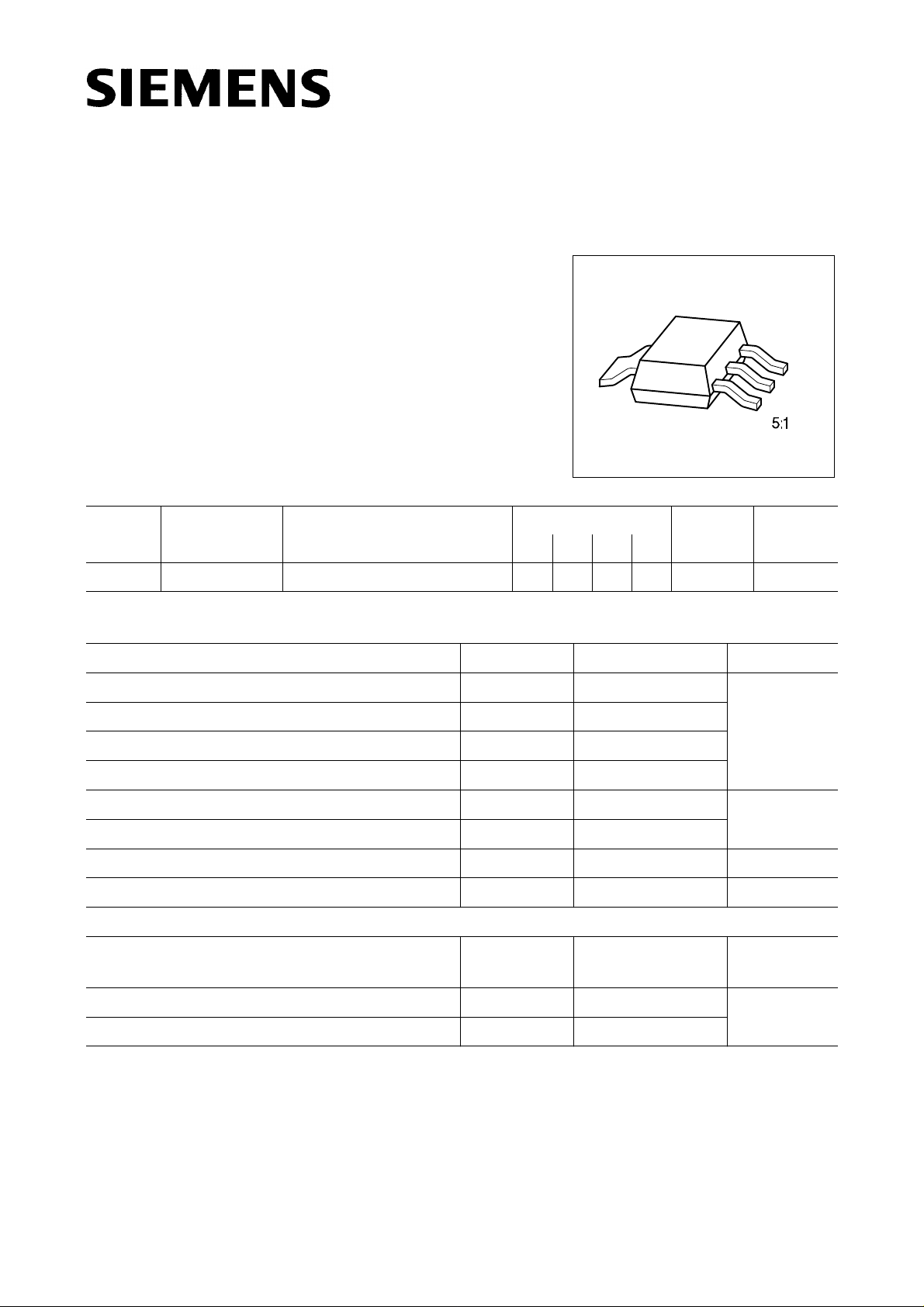
Tape and Reel Information Pin Configuration Marking Package
1234
BSP 149 Q67000-S071 E6327: 1000 pcs/reel G D S D BSP 149 SOT-223
Maximum Ratings
Parameter Symbol Values Unit
Drain-source voltage
Drain-gate voltage,
R
= 20 kΩ V
GS
Gate-source voltage
Gate-source peak voltage, aperiodic
Continuous drain current,
Pulsed drain current,
Max. power dissipation,
T
= 28 ˚C I
A
T
= 25 ˚C I
A
T
= 25 ˚C P
A
Operating and storage temperature range
V
V
V
D
D puls
T
j
DS
DGR
GS
gs
tot
, T
stg
200 V
200
± 14
± 20
0.48 A
1.44
1.8 W
– 55 … + 150 ˚C
Thermal resistance
1)
chip-ambient
chip-soldering point
R
thJA
R
thJS
70
10
K/W
DIN humidity category, DIN 40 040 – E –
IEC climatic category, DIN IEC 68-1 – 55/150/56
1)
Transistor on epoxy pcb 40 mm × 40 mm × 1.5 mm with 6 cm2 copper area for drain connection.
Semiconductor Group 1 09.96
BSP 149
Electrical Characteristics
at Tj = 25 ˚C, unless otherwise specified.
Parameter Symbol Values Unit
min. typ. max.
Static Characteristics
Drain-source breakdown voltage
V
= − 3 V, ID = 0.25 mA
GS
Gate threshold voltage
V
= 3 V, ID = 1 mA
DS
Drain-source cutoff current
V
= 200 V, VGS = − 3 V
DS
T
= 25 ˚C
j
T
= 125 ˚C
j
Gate-source leakage current
V
= 20 V, VDS = 0
GS
Drain-source on-resistance
V
= 0 V, ID = 0.03 A
GS
Dynamic Characteristics
Forward transconductance
V
≥ 2 × ID× R
DS
DS(on)max
, ID = 0.48 A
Input capacitance
V
= 0, VDS = 25 V, f = 1 MHz
GS
Output capacitance
V
= 0, VDS = 25 V, f = 1 MHz
GS
Reverse transfer capacitance
V
= 0, VDS = 25 V, f = 1 MHz
GS
Turn-on time
V
=30V,VGS = − 2 ... + 5V, RGS =50Ω,
DD
I
=0.29 A
D
Turn-off time t
V
=30V,VGS = − 2 ... + 5V, RGS =50Ω,
DD
I
=0.29 A
D
t
, (ton = t
on
, (t
off
+ tr)
d(on)
= t
d(off)
+ tf)
off
V
(BR)DSS
V
GS(th)
I
DSS
I
GSS
R
DS(on)
g
fs
C
iiss
C
oss
C
rss
t
d(on)
t
r
t
d(off)
t
f
V
200 – –
− 1.8 − 1.2 − 0.7
µA
–
–
–
–
0.2
200
nA
– 10 100
Ω
– 2.5 3.5
S
0.4 0.75 –
pF
– 500 670
–4060
–1220
– 7 10 ns
–2030
–6080
–5065
Semiconductor Group 2
BSP 149
Electrical Characteristics (cont’d)
at Tj = 25 ˚C, unless otherwise specified.
Parameter Symbol Values Unit
min. typ. max.
Reverse Diode
Continuous reverse drain current
T
= 25 ˚C
A
Pulsed reverse drain current
T
= 25 ˚C
A
Diode forward on-voltage
I
= 0.96 A, VGS = 0
F
V
Grouping Symbol Limit Values Unit Test Condition
GS(th)
I
S
– – 0.48
I
SM
– – 1.44
V
SD
– 0.9 1.2
min. max.
Range of
Threshold voltage selected in groups
1) A specific group cannot be ordered separately.
Each reel only contains transistors from one group.
V
GS(th)
P
R
S
T
U
V
W
∆V
GS(th)
1)
:
V
GS(th)
– 0.15 V –
– 0.95
– 1.08
– 1.21
– 1.34
– 1.47
– 1.60
– 1.73
– 0.80
– 0.93
– 1.06
– 1.19
– 1.32
– 1.45
– 1.58
V
V
V
V
V
V
V
V
D1
V
D2
I
= 1 mA
D
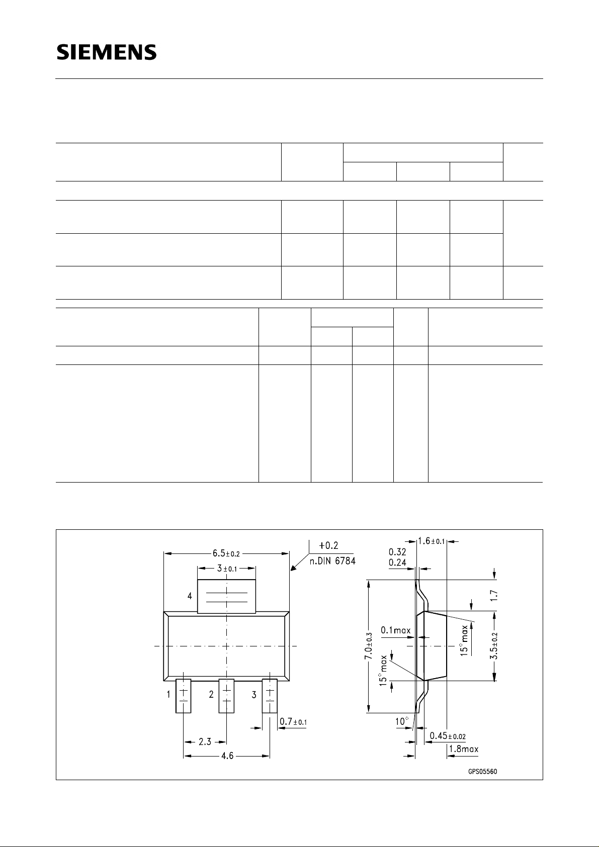
Package Outline
A
V
= 0.2 V;
= 3 V;
SOT-223
Dimensions in mm
Semiconductor Group 3
 Loading...