

Siemens BSM121AR Datasheet
SIMOPAC® Module BSM 121 AR
V
I
R
● Power module
● Single switch
● N channel
● Enhancement mode
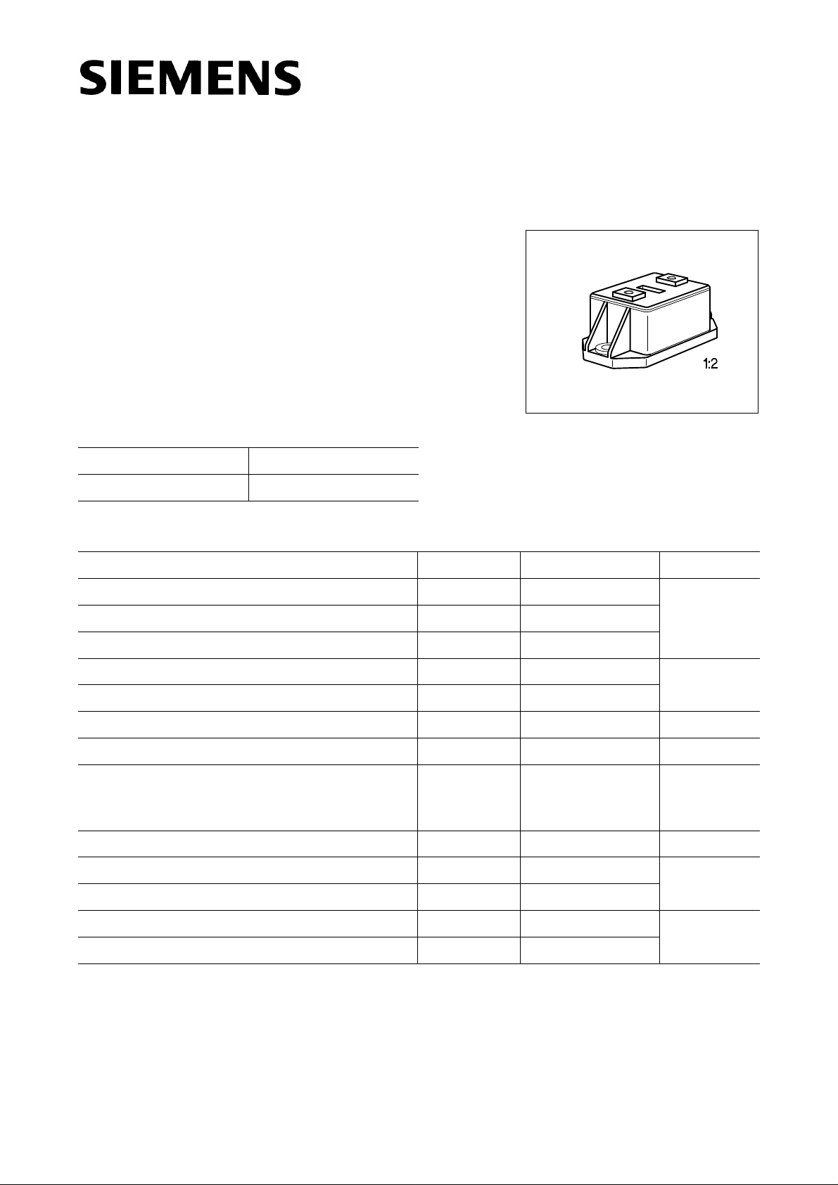
● Package with insulated metal base plate
● Package outline/Circuit diagram: 1
DS
D
DS(on)
= 200 V
= 130 A
= 20 mΩ
1)
Type Ordering Code
BSM 121 AR C67076-S1014-A2
Maximum Ratings
Parameter Symbol Values Unit
Drain-source voltage
Drain-gate voltage,
R
= 20 kΩ V
GS
Gate-source voltage
Continuous drain current,
Pulsed drain current,
T
= 25 ˚C I
C
T
= 25 ˚C I
C
Operating and storage temperature range
Power dissipation,
T
= 25 ˚C P
C
Thermal resistance
Chip-case
Case-heat sink
Insulation test voltage
2)
, t = 1 min. V
V
V
D
D puls
T
j
R
R
DS
DGR
GS
, T
tot
th JC
th CH
is
stg
200 V
200
± 20
130 A
390
– 55 … + 150 ˚C
700 W
K/W
≤ 0.18
≤ 0.05
2500 V
ac
Creepage distance, drain-source – 16 mm
Clearance, drain-source – 11
DIN humidity category, DIN 40 040 – F –
IEC climatic category, DIN IEC 68-1 – 55/150/56
1)
See chapter Package Outline and Circuit Diagrams.
2)
Insulation test voltage between drain and base plate referred to standard climate 23/50 in acc. with
DIN 50 014, IEC 146, para. 492.1.
Semiconductor Group 31 03.96
BSM 121 AR
Electrical Characteristics
at Tj = 25 ˚C, unless otherwise specified.
Parameter Symbol Values Unit
min. typ. max.
Static Characteristics
Drain-source breakdown voltage
V
= 0, ID = 0.25 mA
GS
Gate threshold voltage
V
= VDS, ID = 1 mA
GS
Zero gate voltage drain current
V
= 200 V, VGS = 0
DS
T
= 25 ˚C
j
T
= 125 ˚C
j
Gate-source leakage current
V
= 20 V, VDS = 0
GS
Drain-source on-state resistance
V
= 10 V, ID = 80 A
GS
Dynamic Characteristics
Forward transconductance
V
≥ 2 × ID× R
DS
DS(on)max.
, ID = 80 A
Input capacitance
V
= 0, VDS = 25 V, f = 1 MHz
GS
Output capacitance
V
= 0, VDS = 25 V, f = 1 MHz
GS
Reverse transfer capacitance
V
= 0, VDS = 25 V, f = 1 MHz
GS
t
Turn-on time
V
= 100 V, VGS = 10 V
CC
I
= 80 A, RGS = 3.3 Ω
D
Turn-off time
V
= 100 V, VGS = 10 V
CC
I
= 80 A, RGS = 3.3 Ω
D
(ton = t
on
t
off(toff
= t
d (on)
d (off)
+ tr)
+ tf)
V
(BR)DSS
V
GS(th)
I
DSS
I
GSS
R
DS(on)
g
fs
C
iiss
C
oss
C
rss
t
d (on)
t
r
t
d (off)
t
f
V
200 – –
2.1 3.0 4.0
µA
–
–
50
300
250
1000
nA
– 10 100
mΩ
–1820
60 75 – S
–1013nF
– 3 4.5
– 0.7 1.0
– 120 – ns
–60–
– 240 –
–40–
Semiconductor Group 32
BSM 121 AR
Electrical Characteristics (cont’d)
at Tj = 25 ˚C, unless otherwise specified.
Parameter Symbol Values Unit
min. typ. max.
Reverse diode
Continuous reverse drain current
T
= 25 ˚C
C
Pulsed reverse drain current
T
= 25 ˚C
C
Diode forward on-voltage
I
= 260 A , VGS = 0
F
Reverse recovery time
I
= IS, diF/dt = 100 A/ µs, VR = 100 V
F
Reverse recovery charge
I
= IS, diF/dt = 100 A/ µs, VR = 100 V
F
I
I
V
t
Q
rr
S
SM
SD
rr
A
– – 130
– – 390
V
– 1.05 1.4
ns
– 400 –
µC
– 4.3 –
Semiconductor Group 33
 Loading...