

Siemens BFQ74 Datasheet
NPN Silicon RF Transistor BFQ 74
● For low-noise amplifiers in the GHz range,
and broadband analog and digital applications
in telecommunications systems at collector
currents from 1 mA to 25 mA.
● Hermetically sealed ceramic package.
● HiRel/Mil screening available.
ESD: Electrostatic discharge sensitive device, observe handling precautions!
Type Marking
Ordering Code
(tape and reel)
BFQ 74 Q62702-F78874 Cerec-X
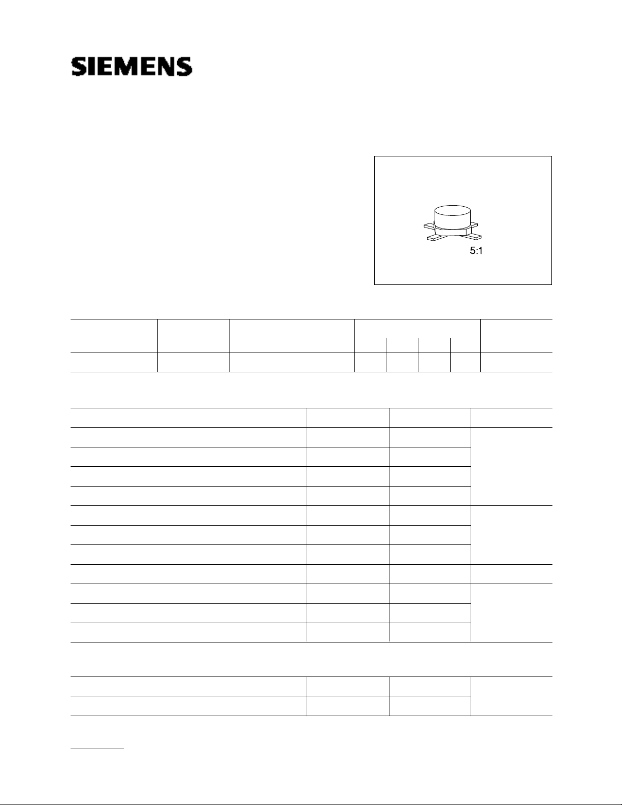
Pin Configuration
1 2 3 4
B E C E
Package
Maximum Ratings
Parameter Symbol Values Unit
Collector-emitter voltage V
CE0 16 V
Collector-emitter voltage, VBE = 0 VCES 25
Collector-base voltage V
CB0 25
Emitter-base voltage VEB0 2
Collector current I
C 35 mA
Peak collector current, f ≥ 10 MHz ICM 45
Base current IB 5
Total power dissipation, T
S ≤ 115 ˚C
3)
Ptot 300 mW
Junction temperature Tj 175 ˚C
1)
Ambient temperature range T
Storage temperature range T
A – 65 … + 175
stg – 65 … + 175
Thermal Resistance
Junction - ambient
Junction - soldering point
1)
For detailed dimensions see chapter Package Outlines.
2)
Package mounted on alumina 15 mm × 16.7 mm × 0.7 mm.
3)
TS is measured on the collector lead at the soldering point to the pcb.
2)
3)
Rth JA ≤ 280 K/W
Rth JS ≤ 200
Electrical Characteristics
A = 25 ˚C, unless otherwise specified.
at T
BFQ 74
BFQ 74
Parameter Symbol
DC Characteristics
V
(BR)CE0 16 – –
C = 1 mA, IB = 0
I
I
CES – – 100
CE = 25 V, VBE = 0
V
I
CB0 ––50
CB = 15 V, IE = 0
V
I
EB0 ––10
EB = 2 V, IC = 0
V
FE
h
I
C = 5 mA, VCE = 10 V
C = 15 mA, VCE = 10 V
I
V
CEsat – 0.13 0.3
C = 30 mA, IB = 3 mA
I
Base-emitter voltage
C = 10 mA, VCE = 10 V
I
V
BE – 0.78 –
min. typ. max.
50
50
110
120
250
–
UnitValues
VCollector-emitter breakdown voltage
µACollector-emitter cutoff current
nACollector-base cutoff current
µAEmitter-base cutoff current
–DC current gain
VCollector-emitter saturation voltage
Electrical Characteristics
A = 25 ˚C, unless otherwise specified.
at T
BFQ 74
BFQ 74
Parameter Symbol
AC Characteristics
T
f
C = 5 mA, VCE = 10 V, f = 200 MHz
I
C = 15 mA, VCE = 10 V, f = 200 MHz
I
C
cb – 0.3 0.4
CB = 10 V, VBE = vbe = 0, f = 1 MHz
V
C
Collector-emitter capacitance
CE = 10 V, VBE = vbe = 0, f = 1 MHz
V
Input capacitance
EB = 0.5 V, IC = ic = 0, f = 1 MHz
V
Output capacitance
CE = 10 V, VBE = vbe = 0, f = 1 MHz
V
ce – 0.4 –
C
ibo – 1.35 –
C
obs – 0.7 –
F
I
C = 3 mA, VCE = 10 V, f = 10 MHz, ZS = 75 Ω
C = 5 mA, VCE = 10 V, f = 800 MHz, ZS = 50 Ω
I
C = 10 mA, VCE = 10 V, f = 2 GHz, ZS = ZSopt
I
min. typ. max.
–
–
–
–
–
4.4
6
0.9
1.4
2.5
–
–
–
–
2.9
UnitValues
GHzTransition frequency
pFCollector-base capacitance
dBNoise figure
Power gain
C = 15 mA, VCE = 10 V, f = 2 GHz, Z0 = 50 Ω
I
C = 15 mA, VCE = 10 V, f = 4 GHz, Z0 = 50 Ω
I
Transducer gain
C = 15 mA, VCE = 10 V, f = 2 GHz, Z0 = 50 Ω
I
two-tone intermodulation test
C = 25 mA, VCE = 10 V, dIM = 60 dB,
I
1 = 806 MHz, f2 = 810 MHz, ZS = ZL = 50 Ω
f
C = 25 mA, VCE = 10 V, f = 800 MHz
I
1)
S21e
(k
–
k2–1)
√
S12e
2)
S21e
S12e
G
G
I S
ma
ms
21e I
1
2
–
)
–
)
2
– 9.8 –
14
9.8
–
–
Vo1 = Vo2 – 160 –
IP
3 –27–
mVLinear output voltage
dBmThird order intercept point
BFQ 74
BFQ 74
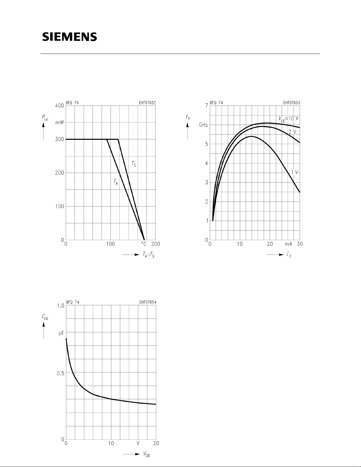
Total power dissipation Ptot = f (TA*; TS)
*Package mounted on alumina
Transition frequency fT = f (IC)
f = 200 MHz
Collector-base capacitance C
BE = vbe = 0, f = 1 MHz
V
cb = f (VCB)
BFQ 74
BFQ 74
Common Emitter Noise Parameters
Γ
f
Fmin Gp(Fmin) RN NF50 Ω Gp(F50Ω)
opt
GHz dB dB MAG ANG Ω –dBdB
IC = 3 mA, VCE = 10 V, Z0 = 50 Ω
0.01 0.7 – (Z
IC = 10 mA, VCE = 10 V, Z0 = 50 Ω
0.01
0.8
2.0
1.05
1.3
2.5
–
17.5
11.5
0.22
0.20
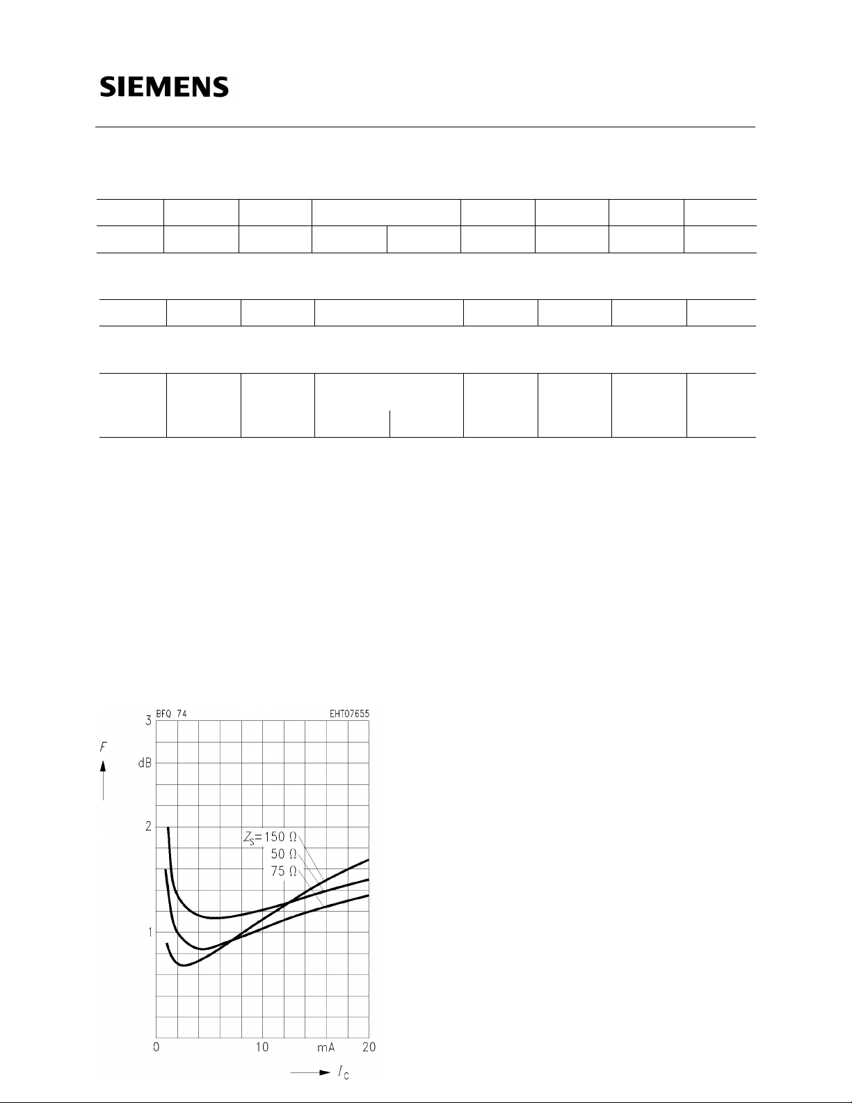
Noise figure F = f (IC)
CE = 10 V, f = 10 MHz
V
S = 150 Ω) – – 1.2 –
S = 75 Ω)
(Z
82
137
–
11.5
23.5
–
0.20
0.60
1.2
1.4
2.7
–
16.8
10
 Loading...