

Siemens BFP520 Datasheet
BFP 520
Semiconductor Group
Sep-09-19981
SIEGET45
NPN Silicon RF Transistor
Preliminary data
• For highest gain low noise amplifier
at 1.8 GHz and 2 mA / 2 V
Outstanding
G
a
= 20 dB
Noise Figure F = 0.95 dB
• For oscillators up to 15 GHz
• Transition frequency
f
T
= 45 GHz
• Gold metalization for high reliability
• SIEGET 45 - Line
Siemens Grounded Emitter Transistor
45 GHz
f
T
- Line
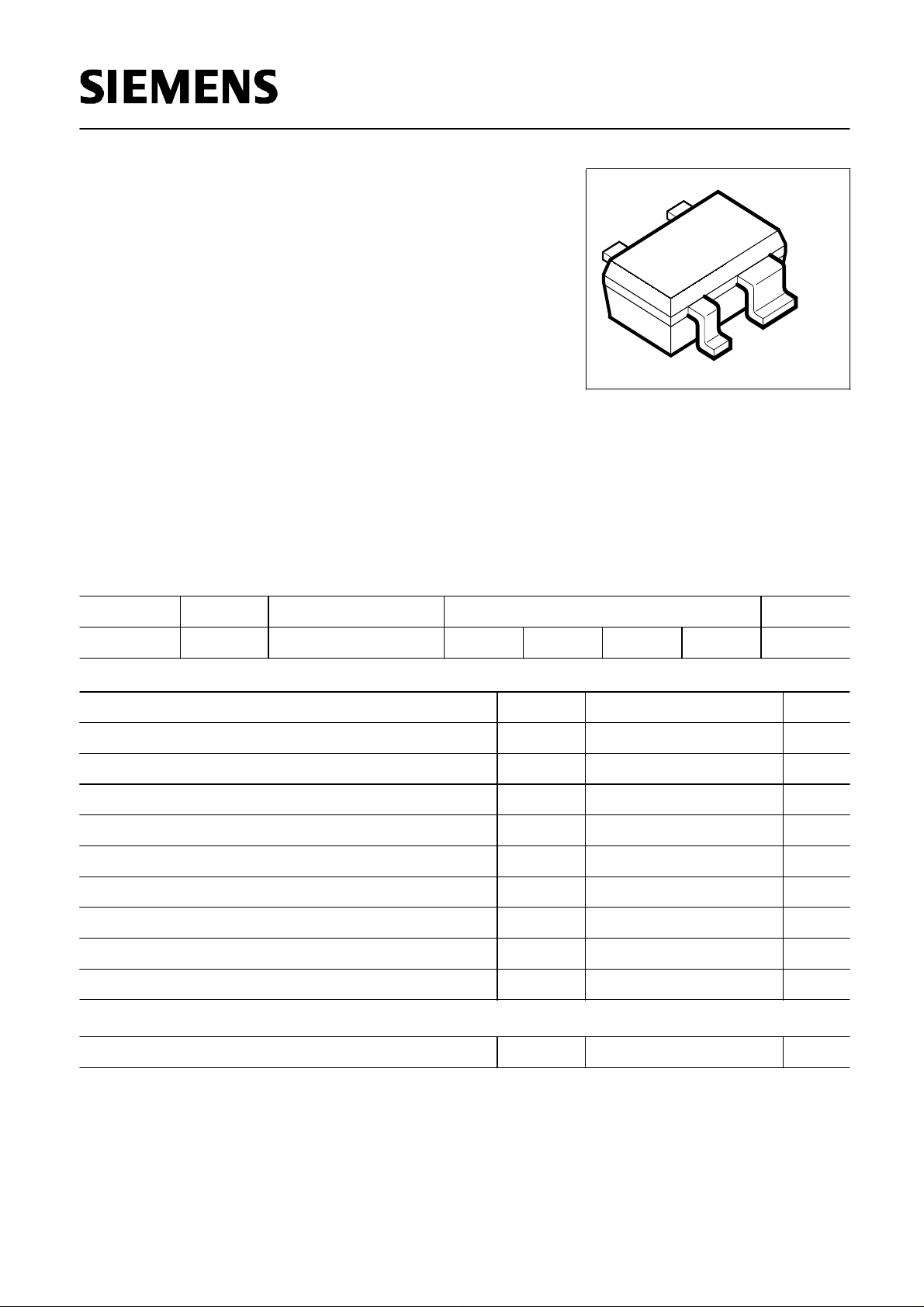
VPS05605
4
2
1
3
ESD: Electrostatic discharge sensitive device, observe handling precaution!
Type Marking Ordering Code Pin Configuration Package
BFP 520 APs Q62702-F1794 1 = B 2 = E 3 = C 4 = E SOT-343
Maximum Ratings
Parameter Symbol Value Unit
Collector-emitter voltage
V
CEO
2.5 V
Collector-base voltage
V
CBO
12 V
Emitter-base voltage
V
EBO
1 V
Collector current
I
C
40 mA
Base current
I
B
4 mA
Total power dissipation,
T
S
≤ 105 °C
P
tot
100 mW
Junction temperature
T
j
150 °C
Ambient temperature
T
A
-65 ...+150 °C
Storage temperature
T
st
g
-65 ...+150 °C
Thermal Resistance
Junction - soldering point
1)
R
thJS
≤ 450
K/W
1) TS is measured on the collector lead at the soldering point to the pcb
Semiconductor Group 1 1998-11-01
BFP 520
Semiconductor Group
Sep-09-19982
Electrical Characteristics at
T
A
= 25°C, unless otherwise specified.
Parameter Symbol Values Unit
min. typ. max.
DC characteristics
Collector-emitter breakdown voltage
I
C
= 1 mA,
I
B
= 0
V
(BR)CEO
2.5 3 3.5 V
Collector-base cutoff current
V
CB
= 5 V,
I
E
= 0
I
CBO
- - 200 nA
Emitter-base cutoff current
V
EB
= 1.5 V,
I
C
= 0
I
EBO
- - 35 nA
DC current gain
I
C
= 20 mA,
V
CE
= 4 V
h
FE
50 80 150
-
AC characteristics
- GHz- 45
f
T
Transition frequency
I
C
= 30 mA,
V
CE
= 2 V, f = 2 GHz
- pF0.06-
C
cb
Collector-base capacitance
V
CB
= 2 V, f = 1 MHz
- pF
C
ce
0.3-
Collector-emitter capacitance
V
CE
= 2 V, f = 1 MHz
-
Emitter-base capacitance
V
EB
= 0.5 V, f = 1 MHz
pF
C
eb
0.35-
-
F
-
Noise figure
I
C
= 2 mA,
V
CE
= 2 V,
Z
S
=
Z
Sopt
,
f
= 1.8 GHz
dB0.95
- dB23-
G
ms
Power gain 1)
I
C
= 20 mA,
V
CE
= 2 V,
Z
S
=
Z
Sopt
,
Z
L
=
Z
Lopt
,
f
= 1.8 GHz
- dB
|
S
21
|
2
Insertion power gain
I
C
= 20 mA,
V
CE
= 2 V, f = 1.8 GHz,
Z
S
=
Z
L
= 50Ω
21-
-
-
Third order intercept point at output
V
CE
= 2 V, f = 1.8 GHz,
Z
S
=
Z
Sopt
,
Z
L
=
Z
Lopt
,
I
C
= 20 mA
I
C
= 7 mA
dBm
IP
3
25
17
-
-
1dB compression point
V
CE
= 2 V, f = 1.8 GHz,
Z
S
=
Z
Sopt
,
Z
L
=
Z
Lopt
,
I
C
= 20 mA
I
C
= 7 mA
dBm
-
-
P
-1dB
-
-
12
5
1)
G
ms
= |
S
21
/
S
12
|
2)
G
ma
= |
S
21
/
S
12
| (k-(k2-1)
1/2
)
Semiconductor Group 2 1998-11-01
BFP 520
Semiconductor Group
Sep-09-19983
Common Emitter S-Parameters
f S
11
S
21
S
12
S
22
GHz MAG ANG MAG ANG MAG ANG MAG ANG
V
CE
= 2 V, /C = 20 mA
0.01
0.1
0.5
1
2
3
4
5
6
0.7244
0.7251
0.6368
0.4768
0.2816
0.225
0.2552
0.3207
0.3675
-0.7
-8.4
-40.7
-73.6
-123.8
-166
156.2
133.6
118.7
32.273
31.637
27.293
19.6
11.02
7.48
5.636
4.488
3.683
178.6
171.4
140.7
113.5
84.9
67.6
53
39.7
27.5
0.0007
0.0041
0.0194
0.0351
0.00574
0.0788
0.0994
0.1177
0.1343
69.4
92.8
75.9
66.5
56.3
49.2
41.5
32.9
24.7
0.9052
0.9363
0.8523
0.6496
0.3818
0.2407
0.1544
0.095
0.0545
1.2
-4.4
-26.7
-46
-64.6
-73.6
-95.3
-128.9
177.6
Common Emitter Noise Parameters
f F
min
1)
G
a
1)
Γ
opt
R
N
r
n
F
50Ω
2)
|
S
21
|
2 2)
GHz dB dB MAG ANG Ω - dB dB
V
CE
= 2 V,
I
C
= 2 mA
0.9
1.8
2.4
3
4
5
6
0.72
0.95
1.07
1.3
1.35
1.7
1.95
21.5
20
16
14.5
11.6
9.5
8
0.64
0.49
0.45
0.4
0.26
0.14
0.12
14
30
41
54
82
128
151
21.5
19
18
16.5
12.5
9
8
0.43
0.38
0.36
0.33
0.25
0.18
0.16
1.75
1.55
1.6
1.7
1.6
1.85
1.95
16.1
15.14
14.07
13.13
11.49
9.87
8.28
V
CE
= 2 V,
I
C
= 5 mA
0.9
1.8
2.4
3
4
5
6
0.89
1.08
1.12
1.32
1.35
1.6
1.8
22
20.5
18
16.2
13.5
11.5
10.5
0.49
0.38
0.34
0.29
0.156
0.08
0.07
12
22
33
45
71
120
150
16
14
14
13.5
11
10
8
0.32
0.28
0.28
0.27
0.22
0.2
0.16
1.5
1.38
1.4
1.5
1.45
1.65
1.8
21.94
19.34
17.54
16.01
13.82
11.93
10.23
1) Input matched for minimum noise figure, output for maximum gain 2)
Z
S
=
Z
L
= 50Ω
For more and detailed S- and Noise-parameters please contact your local Siemens
distributor or sales office to obtain a Siemens Application Notes CD-ROM or see Internet:
http://www.siemens.de/Semiconductor/products/35/35.htm
Semiconductor Group 3 1998-11-01
 Loading...