

Siemens BFP450 Datasheet
BFP 450
Semiconductor Group
Sep-09-19981
SIEGET25
NPN Silicon RF Transistor
• For medium power amplifiers
• Compression point
P
-1dB
= +19 dBm at 1.8 GHz
maximum available gain
G
ma
= 14 dB at 1.8 GHz
Noise figure
F
= 1.25 dB at 1.8 GHz
• Transition frequency
f
T
= 24 GHz
• Gold metalization for high reliability
• SIEGET 25 - Line
Siemens Grounded Emitter Transistor
25 GHz
f
T
- Line
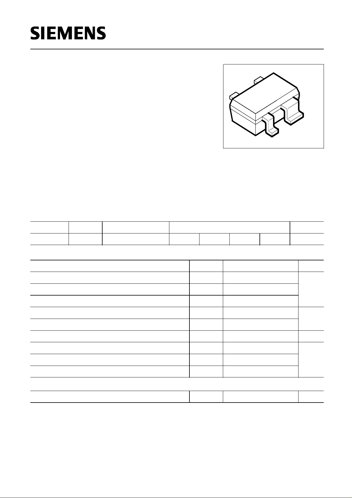
VPS05605
4
2
1
3
ESD: Electrostatic discharge sensitive device, observe handling precaution!
Type Marking Ordering Code Pin Configuration Package
BFP 450 ANs Q62702-F1590 1 = B 2 = E 3 = C 4 = E SOT-343
Maximum Ratings
Parameter Symbol Value Unit
Collector-emitter voltage
V
CEO
V4.5
V
CBO
15Collector-base voltage
V
EBO
Emitter-base voltage 1.5
Collector current 100 mA
I
C
I
B
10Base current
mW450
Total power dissipation,
T
S
≤ 96 °C
P
tot
Junction temperature
T
j
150 °C
T
A
-65 ...+150Ambient temperature
Storage temperature
T
st
g
-65 ...+150
Thermal Resistance
Junction - soldering point
1)
R
thJS
≤ 130
K/W
1) TS is measured on the collector lead at the soldering point to the pcb
Semiconductor Group 1 1998-11-01
BFP 450
Semiconductor Group
Sep-09-19982
Electrical Characteristics at
T
A
= 25°C, unless otherwise specified.
Parameter
Symbol Values Unit
min. typ. max.
DC characteristics
5 6.54.5
V
(BR)CEO
Collector-emitter breakdown voltage
I
C
= 1 mA,
I
B
= 0
V
- 600-
Collector-base cutoff current
V
CB
= 5 V,
I
E
= 0
I
CBO
nA
- 100 µA-
Emitter-base cutoff current
V
EB
= 1.5 V,
I
C
= 0
I
EBO
80
DC current gain
I
C
= 50 mA,
V
CE
= 4 V
h
FE
150
-
50
AC characteristics
Transition frequency
I
C
= 90 mA,
V
CE
= 3 V, f = 1 GHz
I
C
= 90 mA,
V
CE
= 3 V, f = 2 GHz
f
T
-
15
24
17
-
-
GHz
Collector-base capacitance
V
CB
= 2 V, f = 1 MHz
C
cb
- 0.48 0.75 pF
Collector-emitter capacitance
V
CE
= 2 V, f = 1 MHz
C
ce
- 1.33 -
Emitter-base capacitance
V
EB
= 0.5 V, f = 1 MHz
C
eb
- 1.75 -
Noise figure
I
C
= 10 mA,
V
CE
= 2 V,
Z
S
=
Z
Sopt
,
f
= 1.8 GHz
F
- 1.25 1.6 dB
Power gain 2)
I
C
= 50 mA,
V
CE
= 2 V,
Z
S
=
Z
Sopt
,
Z
L
=
Z
Lopt
,
f
= 1.8 GHz
G
ma
- 14 - dB
Insertion power gain
I
C
= 50 mA,
V
CE
= 2 V, f = 1.8 GHz,
Z
S
=
Z
L
= 50Ω
|
S
21
|
2
8 11 -
Third order intersept point
I
C
= 50 mA,
V
CE
= 3 V,
Z
S
=
Z
Sopt
,
Z
L
=
Z
Lopt
,
f
= 1.8 GHz
IP
3
- 29 - dBm
1dB Compression point
I
C
= 50 mA,
V
CE
= 3 V, f = 1.8 GHz,
Z
S
=
Z
Sopt
,
Z
L
=
Z
Lopt
P
-1dB
- 19 -
2)
G
ma
= |
S
21
/
S
12
| (k-(k2-1)
1/2
)
Semiconductor Group 2 1998-11-01
BFP 450
Semiconductor Group
Sep-09-19983
Common Emitter S-Parameters
f S
11
S
21
S
12
S
22
GHz MAG ANG MAG ANG MAG ANG MAG ANG
V
CE
= 2V,
I
C
= 50mA
0.01
0.1
0.5
1
2
3
4
5
6
0.143
0.469
0.681
0.705
0.73
0.752
0.783
0.797
0.813
-30.7
-121.7
-172.4
173.1
154.7
139.5
124.1
112.5
103.7
69.9
51.98
14.86
7.26
3.42
2.22
1.62
1.23
1.01
174.8
125.6
90.7
74.6
55
38.4
22.4
8.8
-2.9
0.0018
0.0139
0.0289
0.047
0.08
0.1183
0.1461
0.1633
0.1864
85.2
59.6
51.4
55.7
51.2
42
30.3
20.7
12.6
0.904
0.744
0.466
0.464
0.491
0.529
0.587
0.606
0.625
-6.6
-64.2
-146.1
-172.2
163.6
145.5
131.9
119.5
108.9
Common Emitter Noise Parameters
f F
min
1)
G
a
1)
Γ
opt
R
N
r
n
F
50Ω
2)
|
S
21
|
2 2)
GHz dB dB MAG ANG Ω - dB dB
V
CE
= 2V,
I
C
= 10mA
0.9
1.8
2.4
3
4
0.9
1.25
1.45
1.7
2.1
15.5
11.8
10.9
8.5
6.6
0.29
0.47
0.56
0.62
0.66
175
-171
-159
-147
-127
2.7
3
3.5
5.5
15.5
0.054
0.06
0.07
0.11
0.31
0.98
1.74
2.23
3.05
4.49
16
9.5
6.8
4.7
1.9
1) Input matched for minimum noise figure, output for maximum gain 2)
Z
S
=
Z
L
= 50Ω
For more and detailed S- and Noise-parameters please contact your local Siemens
distributor or sales office to obtain a Siemens Application Notes CD-ROM or see Internet:
http://www.siemens.de/Semiconductor/products/35/35.htm
Semiconductor Group 3 1998-11-01
 Loading...