

Siemens BFP420 Datasheet
BFP 420
Semiconductor Group
Jul-14-19981
SIEGET25
NPN Silicon RF Transistor
• For high gain low noise amplifiers
• For oscillators up to 10 GHz
• Noise figure
F
= 1.05 dB at 1.8 GHz
outstanding
G
ms
= 20 dB at 1.8 GHz
• Transition frequency
f
T
= 25 GHz
• Gold metalization for high reliability
• SIEGET 25 - Line
Siemens Grounded Emitter Transistor
25 GHz
f
T
- Line
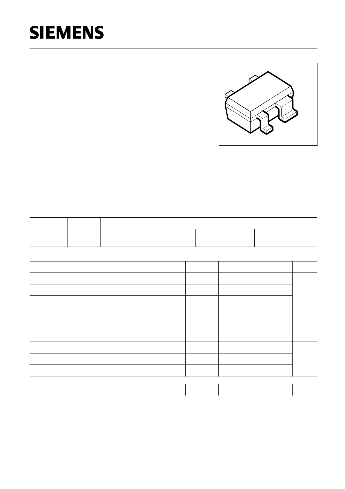
VPS05605
4
2
1
3
ESD: Electrostatic discharge sensitive device, observe handling precaution!
Type Marking Ordering Code Pin Configuration Package
BFP 420 AMs Q62702-F1591 1 = B 2 = E 3 = C 4 = E SOT-343
Maximum Ratings
Parameter
Symbol Value Unit
Collector-emitter voltage
V
CEO
V4.5
V
CBO
15Collector-base voltage
V
EBO
Emitter-base voltage 1.5
Collector current 35 mA
I
C
I
B
3Base current
mW160
Total power dissipation,
T
S
≤ 107 °C
P
tot
Junction temperature
T
j
150 °C
T
A
-65 ...+150Ambient temperature
Storage temperature
T
stg
-65 ...+150
Thermal Resistance
Junction - soldering point
1)
R
thJS
≤ 270
K/W
1) TS is measured on the collector lead at the soldering point to the pcb
Semiconductor Group 1 1998-11-01
BFP 420
Semiconductor Group
Jul-14-19982
Electrical Characteristics at
T
A
= 25°C, unless otherwise specified.
Parameter
Symbol Values Unit
min. typ. max.
DC characteristics
5 6.54.5
V
(BR)CEO
Collector-emitter breakdown voltage
I
C
= 1 mA,
I
B
= 0
V
- 200-
Collector-base cutoff current
V
CB
= 5 V,
I
E
= 0
I
CBO
nA
- 35 µA-
Emitter-base cutoff current
V
EB
= 1.5 V,
I
C
= 0
I
EBO
80
DC current gain
I
C
= 20 mA,
V
CE
= 4 V
h
FE
150
-
50
AC characteristics
Transition frequency
I
C
= 30 mA,
V
CE
= 3 V, f = 2 GHz
f
T
20 25 - GHz
Collector-base capacitance
V
CB
= 2 V, f = 1 MHz
C
cb
- 0.15 0.24 pF
Collector-emitter capacitance
V
CE
= 2 V, f = 1 MHz
C
ce
- 0.41 -
Emitter-base capacitance
V
EB
= 0.5 V, f = 1 MHz
C
eb
- 0.55 -
Noise figure
I
C
= 5 mA,
V
CE
= 2 V,
Z
S
=
Z
Sopt
,
f
= 1.8 GHz
F
- 1.05 1.4 dB
Power gain 1)
I
C
= 20 mA,
V
CE
= 2 V,
Z
S
=
Z
Sopt
,
Z
L
=
Z
Lopt
,
f
= 1.8 GHz
G
ms
- 20 -
Insertion power gain
I
C
= 20 mA,
V
CE
= 2 V, f = 1.8 GHz,
Z
S
=
Z
L
= 50Ω
|
S
21
|
2
14 17 - dB
Third order intersept point
I
C
= 20 mA,
V
CE
= 2 V,
Z
S
=
Z
Sopt
,
Z
L
=
Z
Lopt
,
f
= 1.8 GHz
IP
3
- 22 - dBm
1dB Compression point
I
C
= 20 mA,
V
CE
= 2 V, f = 1.8 GHz,
Z
S
=
Z
Sopt
,
Z
L
=
Z
Lopt
P
-1dB
- 12 -
1)
G
ms
= |
S
21
/
S
12
|
Semiconductor Group 2 1998-11-01
BFP 420
Semiconductor Group
Jul-14-19983
Common Emitter S-Parameters
f S
11
S
21
S
12
S
22
GHz MAG ANG MAG ANG MAG ANG MAG ANG
V
CE
= 2V,
I
C
= 20mA
0.01
0.1
0.5
1
2
3
4
6
8
9
10
0.543
0.538
0.448
0.417
0.437
0.472
0.53
0.617
0.73
0.788
0.82
-2.5
-25.1
-99.3
-143.6
176.2
152.8
133.3
109.1
82.5
72.6
67
36.88
35.4
22.87
13.46
6.93
4.59
3.339
2.15
1.46
1.2
1
178.1
164.4
120.8
96.3
71.5
54.4
38.9
12.9
-16.8
-30.4
-39.5
0.0009
0.0075
0.0272
0.0398
0.062
0.09
0.115
0.156
0.172
0.174
0.172
95.8
79.3
58.7
55.2
53.5
48.6
40.5
25.3
5.4
-5
-11.3
0.96
0.946
0.633
0.399
0.227
0.134
0.109
0.136
0.229
0.319
0.405
-0.6
-12.3
-45.2
-60.3
-77.1
-96.7
-144.5
144.1
101.3
86.1
78.6
Common Emitter Noise Parameters
f F
min
1)
G
a
1)
Γ
opt
R
N
r
n
F
50Ω
2)
|
S
21
|
2 2)
GHz dB dB MAG ANG Ω - dB dB
V
CE
= 2V,
I
C
= 5mA
0.9
1.8
2.4
3
4
5
6
0.9
1.05
1.25
1.38
1.55
1.75
2.2
20.5
15.2
13
12.1
10.3
8.6
6.4
0.19
0.11
0.11
0.19
0.28
0.37
0.44
30
64
116
165
-155
-130
-117
8.7
7.5
7
6.5
7
10
15
0.17
0.15
0.14
0.13
0.14
0.2
0.3
1.02
1.11
1.32
1.48
1.83
2.2
3.3
20.3
15.8
13.5
11.6
9.1
7
5.3
1) Input matched for minimum noise figure, output for maximum gain 2)
Z
S
=
Z
L
= 50Ω
For more and detailed S- and Noise-parameters please contact your local Siemens
distributor or sales office to obtain a Siemens Application Notes CD-ROM or see Internet:
http://www.siemens.de/Semiconductor/products/35/35.htm
Semiconductor Group 3 1998-11-01
 Loading...