

Siemens BF998 Datasheet
Silicon N Channel MOSFET Tetrode BF 998
Features
● Short-channel transistor
with high S/C quality factor
● For low-noise, gain-controlled
input stages up to 1 GHz
Type Marking
Ordering Code
(tape and reel)
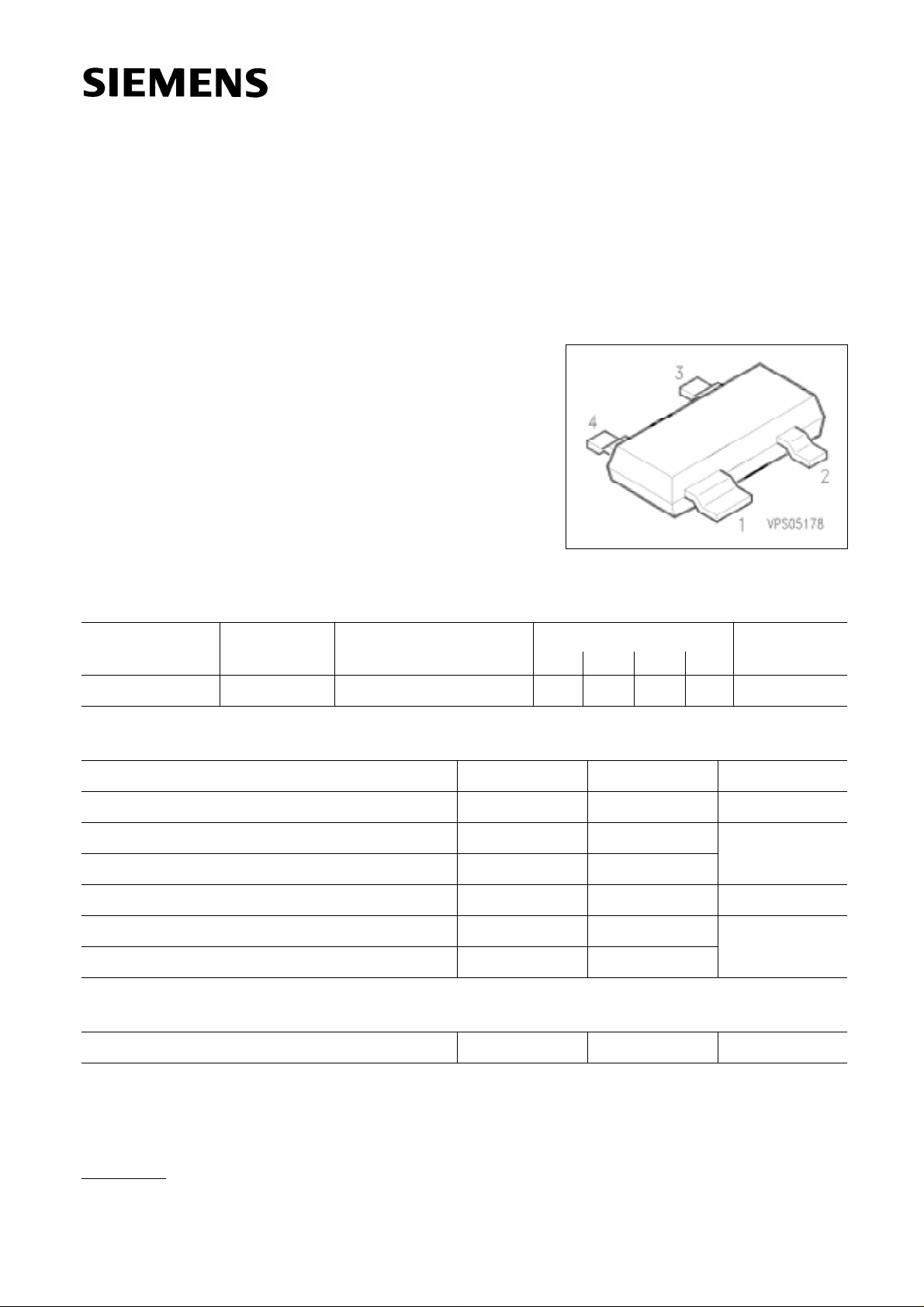
BF 998 Q62702-F1129MO SOT-143
Pin Configuration
1 2 3 4
S D G2 G1
Package
Maximum Ratings
Parameter Symbol Values Unit
Drain-source voltage V
DS 12 V
mADrain current ID 30
Gate 1/gate 2 peak source current
± IG1/2SM 10
Total power dissipation, TS < 76 ˚C Ptot 200 mW
Storage temperature range T
stg – 55 … + 150 ˚C
Channel temperature Tch 150
Thermal Resistance
th JS < 370 K/W
Junction - soldering point
R
1)
1)
For detailed information see chapter Package Outlines.
Semiconductor Group 1 04.96
Electrical Characteristics
I
A = 25 ˚C, unless otherwise specified.
at T
BF 998
Parameter Symbol
DC Characteristics
V
(BR) DS 12 – –
D = 10 µA, – VG1S = – VG2S = 4 V
Gate 1-source breakdown voltage
±IG1S = 10 mA, VG2S = VDS = 0
Gate 2-source breakdown voltage
±IG2S = 10 mA, VG1S = VDS = 0
±VG1S = 5 V, VG2S = VDS = 0
Gate 2-source leakage current
±VG2S = 5 V, VG1S = VDS = 0
DS = 8 V, VG1S = 0, VG2S = 4 V
V
DS = 8 V, VG2S = 4 V, ID = 20 µA
V
± V(BR) G1SS 8–12
± V(BR) G2SS 8–12
± IG1SS ––50
± IG2SS ––50
I
DSS 2–18
– V
G1S(p) – – 2.5
UnitValues
min. typ. max.
VDrain-source breakdown voltage
nAGate 1-source leakage current
mADrain current
VGate 1-source pinch-off voltage
Gate 2-source pinch-off voltage
DS = 8 V, VG1S = 0, ID = 20 µA
V
– V
G2S(p) ––2
Semiconductor Group 2
Electrical Characteristics
A = 25 ˚C, unless otherwise specified.
at T
BF 998
Parameter
AC Characteristics
Forward transconductance
DS = 8 V, ID = 10 mA, VG2S = 4 V
V
f = 1 kHz
DS = 8 V, ID = 10 mA, VG2S = 4 V
V
f = 1 MHz
Gate 2 input capacitance
DS = 8 V, ID = 10 mA, VG2S = 4 V
V
f = 1 MHz
DS = 8 V, ID = 10 mA, VG2S = 4 V
V
f = 1 MHz
DS = 8 V, ID = 10 mA, VG2S = 4 V
V
f = 1 MHz
Symbol
min.–typ.
fs
g
g1ss – 2.1 2.5
C
g2ss – 1.2 –
C
dg1 –25–
C
dss – 1.05 –
C
24
max.
–
UnitValues
mS
pFGate 1 input capacitance
fFReverse transfer capacitance
pFOutput capacitance
(test circuit 1)
DS = 8 V, ID = 10 mA, f = 200 MHz,
V
G = 2 mS, GL = 0.5 mS, VG2S = 4 V
G
Power gain
(test circuit 2)
DS = 8 V, ID = 10 mA, f = 800 MHz,
V
G = 3.3 mS, GL = 1 mS, VG2S = 4 V
G
(test circuit 1)
DS = 8 V, ID = 10 mA, f = 200 MHz,
V
G = 2 mS, GL = 0.5 mS, VG2S = 4 V
G
Noise figure
(test circuit 2)
DS = 8 V, ID = 10 mA, f = 800 MHz,
V
G = 3.3 mS, GL = 1 mS, VG2S = 4 V
G
Control range
(test circuit 2)
DS = 8 V, VG2S = 4 … – 2 V
V
f = 800 MHz
Gps –28–
Gps –20–
F – 0.6 –
F –1–
∆Gps 40 – –
dBPower gain
dBNoise figure
Semiconductor Group 3
 Loading...