

Siemens BF987 Datasheet
Silicon N Channel MOSFET Triode BF 987
● For high-frequency stages up to 300 MHz,
preferably in FM applications
● High overload capability
Type Marking
Ordering Code
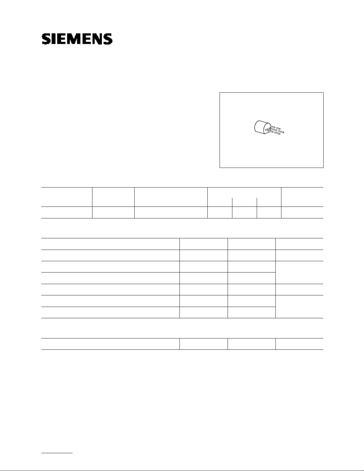
Pin Configuration
Package
1 2 3
BF 987 Q62702-F35– TO-92
D S G
Maximum Ratings
Parameter Symbol Values Unit
Drain-source voltage V
DS 20 V
mADrain current ID 30
Gate-source peak current
± IGSM 10
Total power dissipation, TA ≤ 45 ˚C Ptot 300 mW
Storage temperature range T
stg – 55 … + 150 ˚C
Channel temperature Tch 150
Thermal Resistance
Junction - ambient Rth JA ≤ 350 K/W
1)
1)
For detailed information see chapter Package Outlines.
Electrical Characteristics
A = 25 ˚C, unless otherwise specified.
at T
BF 987
Parameter Symbol
DC Characteristics
V
(BR) DS 20 – –
D = 10 µA, – VGS = 4 V
I
Gate-source breakdown voltage
± IGS = 10 mA, VDS = 0
± VGS = 5 V, VDS = 0
DS = 10 V, VGS = 0
V
DS = 10 V, ID = 20 µA
V
± V(BR) GSS 6.5 – 12
± IGSS ––50
I
DSS 5–18
– V
GS (p) – – 2.5
AC Characteristics
g
fs 14 16 –
DS = 10 V, ID = 10 mA, f = 1 kHz
V
UnitValues
min. typ. max.
VDrain-source breakdown voltage
nAGate-source leakage current
mADrain current
VGate-source pinch-off voltage
mSForward transconductance
DS = 10 V, ID = 10 mA, f = 1 MHz
V
VDS = 10 V, ID = 10 mA, f = 1 MHz
DS = 10 V, ID = 10 mA, f = 1 MHz
V
DS = 10 V, ID = 10 mA,f = 200 MHz,
V
G = 2 mS, GL = 0.5 mS
G
Noise figure (test circuit)
V
DS = 10 V, ID = 10 mA,f = 200 MHz,
G = 2 mS, GL = 0.5 mS
G
C
gss – 2.7 –
C
dg –35–
C
dss –1–
p –25–
G
F –1–
pFGate input capacitance
fFReverse transfer capacitance
pFOutput capacitance
dBPower gain (test circuit)
 Loading...