

Siemens BF959 Datasheet
NPN Silicon RF Transistor BF 959
● For SAW filter driver applications
in TV tuners
● For linear broadband VHF amplifier
stages
● For oscillator applications
Type Marking
Ordering Code
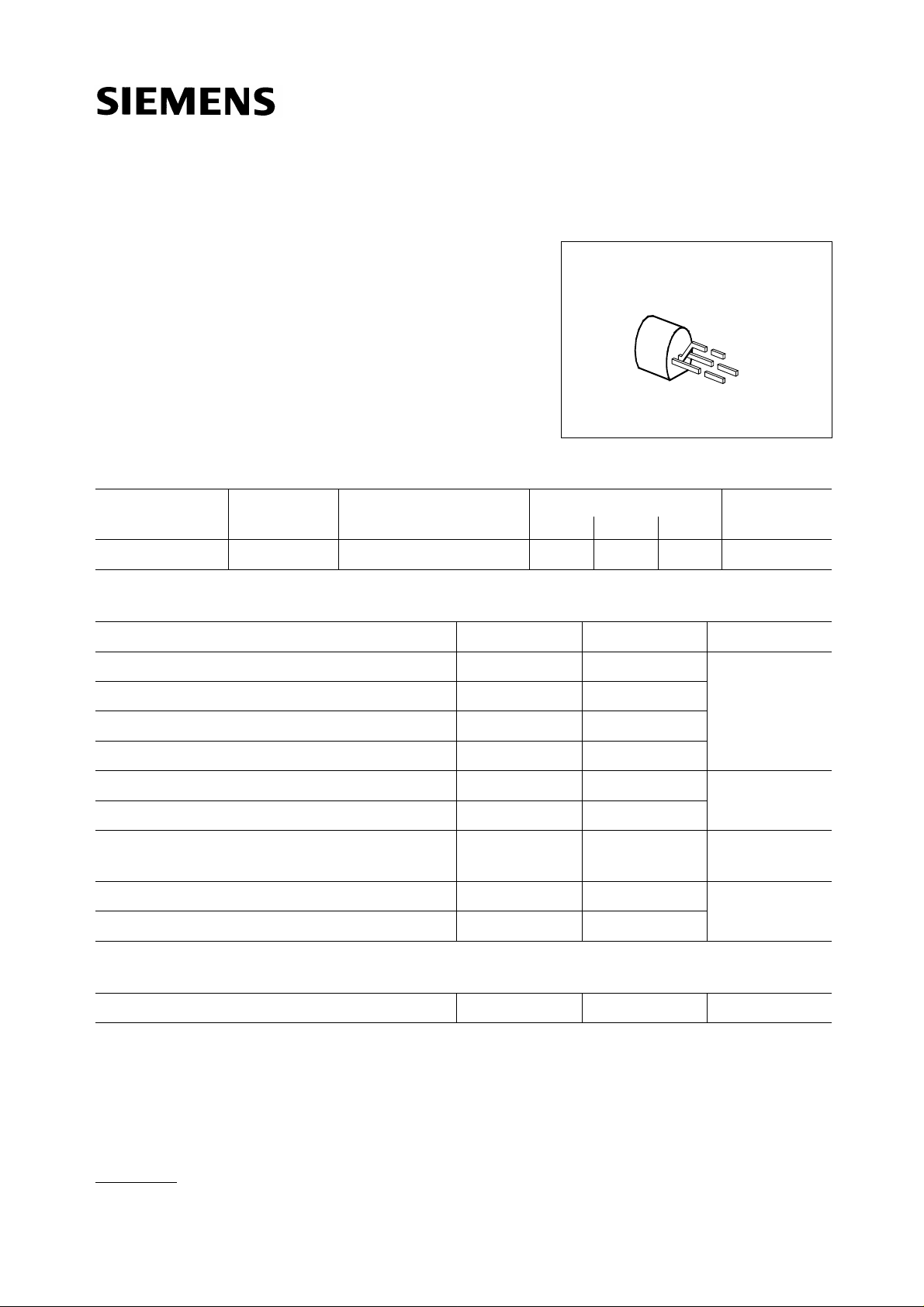
Pin Configuration
Package
1 2 3
BF 959 Q62702-F640– TO-92
C E B
Maximum Ratings
Parameter Symbol Values Unit
Collector-emitter voltage V
CE0 20 V
Collector-emitter reverse voltage VCES 30
Collector-base voltage VCB0 30
Emitter-base voltage V
Peak collector current ICM 100
Peak base current I
Total power dissipation, TA ≤ 25 ˚C
CE ≤ 15 V
V
Junction temperature T
Storage temperature range T
EB0 3
BM 30
P
tot 500 mW
j 150 ˚C
stg – 55 … + 150
mA
1)
Thermal Resistance
Junction - ambient Rth JA ≤ 250 K/W
1)
For detailed information see chapter Package Outlines.
Semiconductor Group 1
Electrical Characteristics
A = 25 ˚C, unless otherwise specified.
at T
BF 959
BF 959
Parameter Symbol
DC Characteristics
V
(BR) CE0 20 – –
C = 1 mA
I
Collector-base breakdown voltage
C = 10 µA
I
Emitter-base breakdown voltage
E = 10 µA
I
V
(BR) CB0 30 – –
V
(BR) EB0 3––
I
CB0 – – 100
V = 20 V
CE = 10 V
C = 5 mA
I
C = 20 mA
I
C = 20 mA, VCE = 10 V
I
Collector-emitter saturation voltage
C = 30 mA, IB = 2 mA
I
FE
h
V
BE – 0.75 –
V
CE sat ––1
min. typ. max.
35
40
–
85
–
–
UnitValues
VCollector-emitter breakdown voltage
nACollector cutoff current
–DC current gain, V
VBase-emitter voltage
Base-emitter saturation voltage
C = 30 mA, IB = 2 mA
I
AC Characteristics
C = 20 mA, VCE = 10 V, f = 100 MHz
I
C = 30 mA, VCE = 5 V
I
CB = 10 V, IE = 0, f = 1 MHz
V
Collector-base capacitance
V
CE = 10 V, VBE = 0, f = 1 MHz
CE = 10 V, f = 200 MHz, RS = 60 Ω
V
C = 5 mA
I
C = 20 mA
I
C = 20 mA, VCE = 10 V, f = 35 MHz
I
V
BE sat – – 0.95
T
f
700
600
C
obo – 0.9 –
C
cb – 0.75 –
1100––
–
F
–
–
g
22e – 0.06 –
3
4
–
–
MHzTransition frequency
pFOutput capacitance
dBNoise figure
mSOutput conductance
Semiconductor Group 2
 Loading...