

Siemens BF841, BF840 Datasheet
NPN Silicon RF Transistors BF 840
BF 841
● Suitable for common emitter RF, IF amplifiers
● Low collector-base
capacitance due to contact shield diffusion
● Low output conductance
Type Ordering CodeMarking
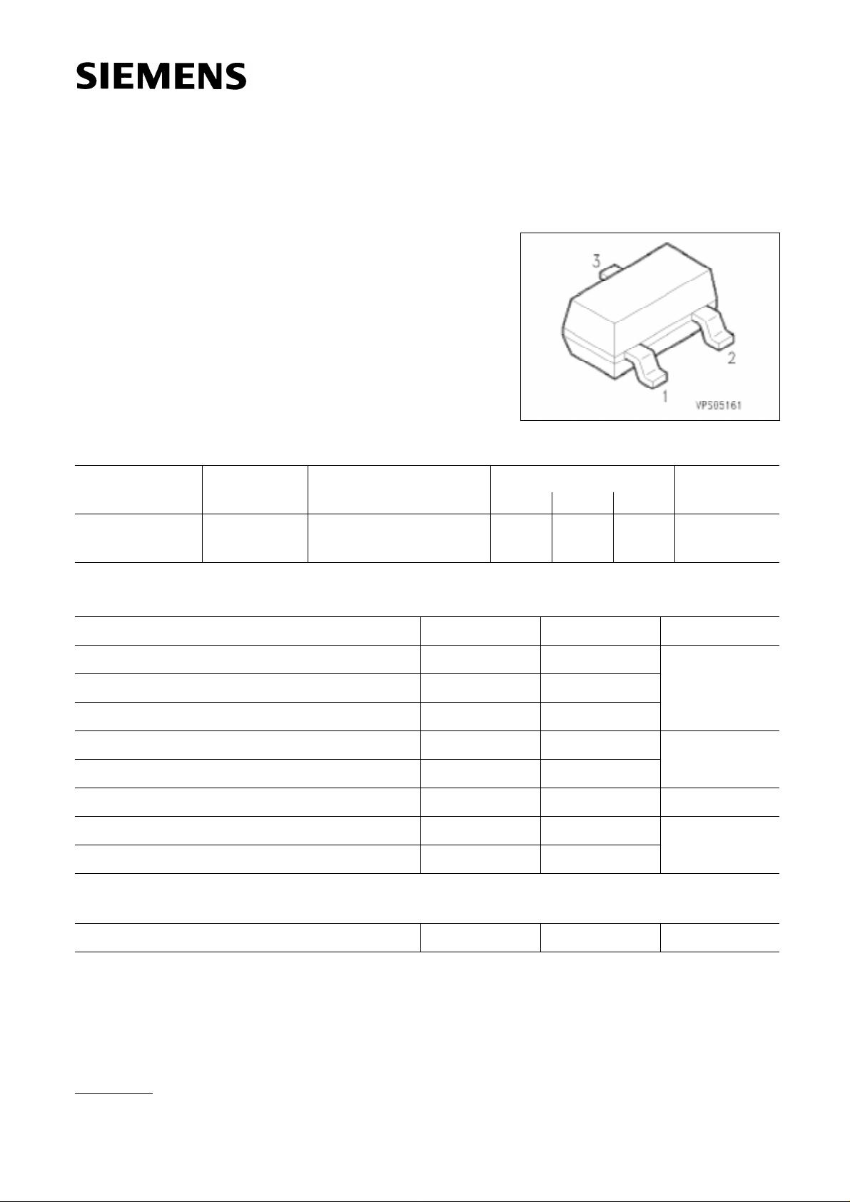
Pin Configuration
Package
1 2 3
BF 840 Q62702-F1240NC SOT-23
B E C
BF 841 Q62702-F1287ND
Maximum Ratings
Parameter Symbol Values Unit
Collector-emitter voltage V
CE0 40 V
Collector-base voltage VCB0 40
Emitter-base voltage V
EB0 4
Collector current IC 25 mA
Base current IB 2
Total power dissipation, TA ≤ 25 ˚C
2)
Junction temperature T
Storage temperature range T
Ptot 280 mW
j 150 ˚C
stg – 65 … + 150
1)
Thermal Resistance
Junction - ambient
1)
For detailed information see chapter Package Outlines.
2)
Package mounted on alumina 15 mm× 16.7 mm × 0.7 mm.
Semiconductor Group 1
2) Rth JA ≤ 450 K/W
07.94
Electrical Characteristics
I
I
I
I
I
R
I
A = 25 ˚C, unless otherwise specified.
at T
BF 840
BF 840
BF 841
Parameter Symbol
DC Characteristics
V
(BR) CE0 40 – –
C = 1 mA, IB = 0
Emitter-base breakdown voltage
E = 10 µA, IB = 0
CB = 20 V, IE = 0
V
C = 1 mA, VCE = 10 V
V
(BR) EB0 4––
I
CB0 – – 100
FE
h
BF 840
BF 841
V
BE – 0.7 –
C = 1 mA, VCE = 10 V
AC Characteristics
min. typ. max.
65
35
–
–
220
125
UnitValues
VCollector-emitter breakdown voltage
nACollector-base cutoff current
–DC current gain, I
VBase-emitter voltage
f
T – 380 –
C = 1 mA, VCE = 10 V, f = 100 MHz
C
CB = 10 V, VBE = vbe = 0, f = 1 MHz
V
cb – 0.3 –
F – 1.7 –
C = 1 mA, VCE = 10 V, f = 100 kHz
S = 200 Ω
C = 1 mA, VCE = 10 V, f = 0.5 MHz
g
22e –4–
MHzTransition frequency
pFCollector-base capacitance
dBNoise figure
µSOutput conductance
Semiconductor Group 2
 Loading...