

Siemens BF799 Datasheet
NPN Silicon RF Transistor BF 799
● For linear broadband amplifier
applications up to 500 MHz
● SAW filter driver in TV tuners
Type Marking
Ordering Code
(tape and reel)
BF 799 Q62702-F935LK SOT-23
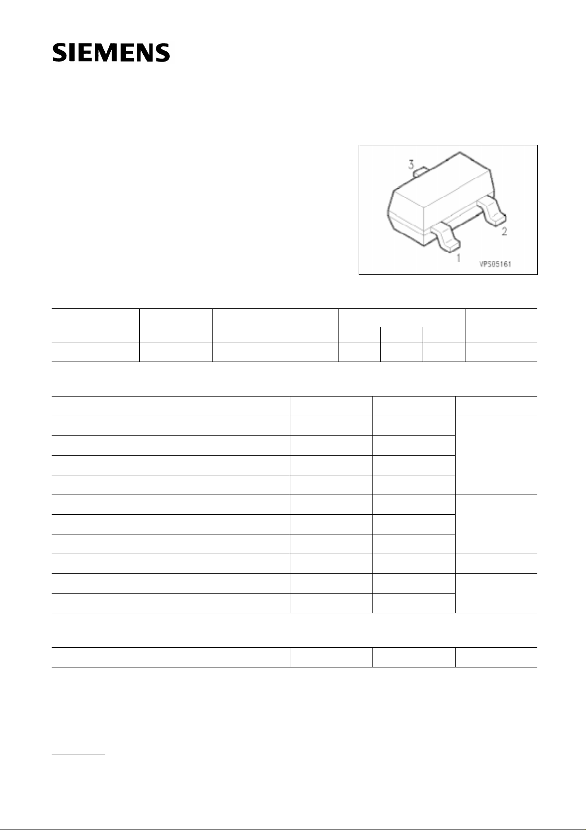
Pin Configuration
1 2 3
B E C
Package
Maximum Ratings
Parameter Symbol Values Unit
Collector-emitter voltage V
CE0 20 V
Collector-emitter reverse voltage VCES 30
Collector-base voltage VCB0 30
Emitter-base voltage V
EB0 3
Collector current IC 35 mA
Peak collector current ICM 50
Peak base current IBM 15
Total power dissipation, TA ≤ 25 ˚C Ptot 280 mW
Junction temperature T
j 150 ˚C
1)
Storage temperature range T
Thermal Resistance
Junction - ambient
1)
For detailed information see chapter Package Outlines.
2)
Package mounted on alumina 15 mm× 16.7 mm × 0.7 mm.
Semiconductor Group 1
2)
stg – 65 … + 150
Rth JA ≤ 450 K/W
07.94
Electrical Characteristics
I
I
I
I
I
I
I
I
I
I
I
R
A = 25 ˚C, unless otherwise specified.
at T
BF 799
Parameter Symbol
UnitValues
min. typ. max.
DC Characteristics
V
(BR) CE0 20 – –
C = 1 mA, IB = 0
Collector-base breakdown voltage
C = 10 µA, IE = 0
Emitter-base breakdown voltage
E = 10 µA
CB = 20 V
V
C = 5 mA
C = 20 mA
CE = 10 V
C = 20 mA, IB = 2 mA
V
(BR) CB0 30 – –
V
(BR) EB0 3––
I
CB0 – – 100
FE
h
35
40
V
CE sat – 0.15 0.5
95
100
–
250
VCollector-emitter breakdown voltage
nACollector cutoff current
–DC current gain, V
VCollector-emitter saturation voltage
Base-emitter saturation voltage
C = 20 mA, IB = 2 mA
V
BE sat – – 0.95
AC Characteristics
C = 5 mA, VCE = 10 V, f = 100 MHz
C = 20 mA, VCE = 8 V, f = 100 MHz
CB = 10 V, f = 1 MHz, IE = 0
V
Collector-base capacitance
T
f
–
–
C
ob – 0.96 –
C
cb – 0.7 –
800
1100––
MHzTransition frequency
pFOutput capacitance
VCB = 10 V, VBE = 0 V, f = 1 MHz
Collector-emitter capacitance
CE = 10 V, VBE = 0 V, f = 1 MHz
V
C = 5 mA, VCE = 10 V, f = 100 MHz
S = 50 Ω
C = 20 mA, VCE = 10 V, f = 35 MHz
C
ce – 0.28 –
F –3–
g
22e –60–
dBNoise figure
µSOutput conductance
Semiconductor Group 2
 Loading...