

Siemens BB689 Datasheet
BB 689
Semiconductor Group
Mar-11-19981
Silicon Tuning Diode
Preliminary data
• For VHF 2-Band-hyperband-TV-tuners
• Very high capacitance ratio
• Low series inductance
• Low series resistance
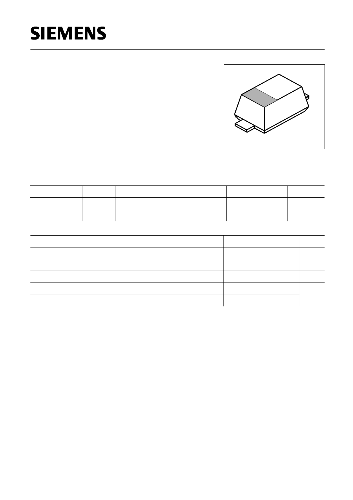
• Extremely small plastic SMD package
• Excellent uniformity and matching due to
"in-line" matching assembly procedure
1
VES05991
2
Type Marking Ordering Code
Pin Configuration
Package
BB 689
BB 689
E
E
Q62702-B0886 unmached
Q62702-B0890 in-line matched
1 = C 2 = A SCD-80
Maximum Ratings
Parameter
ValueSymbol Unit
V
V
R
30
Diode reverse voltage
Peak reverse voltage (R ≥ 5kΩ)
35
V
RM
I
F
20
Forward current
mA
Operating temperature range
T
op
- 55 ...+150
°C
Storage temperature
T
stg
- 55 ...+150
Semiconductor Group 1 1998-11-01
BB 689
Semiconductor Group
Mar-11-19982
Electrical Characteristics at
T
A
= 25°C, unless otherwise specified.
Parameter
ValuesSymbol Unit
typ. max.min.
DC characteristics
I
R
-
- nA
Reverse current
V
R
= 30 V
10
I
R
Reverse current
V
R
= 30 V,
T
A
= 85 °C
- - 200 µA
AC characteristics
61.5
47.2
3
2.9
Diode capacitance
V
R
= 1 V, f = 1 MHz
V
R
= 2 V, f = 1 MHz
V
R
= 25 V, f = 1 MHz
V
R
= 28 V, f = 1 MHz
pF
C
T
56.5
43.4
2.8
2.7
51
39.6
2.6
2.5
Capacitance ratio
V
R
= 2 V,
V
R
= 25 V, f = 1 MHz
C
T2
/
C
T25
-1715.514.5
Capacitance ratio
V
R
= 1 V,
V
R
= 28 V, f = 1 MHz
20.9 23.218
C
T1
/
C
T28
-
∆
C
T
/
C
T
-Capacitance ratio 1)
V
R
= 1 V,
V
R
= 28 V, f = 1 MHz
%2
0.85
r
s
-Series resistance
V
R
= 8 V, f = 470 MHz
-
Ω
Series inductance chip to ground
L
s
- 0.6 - nH
1) In-line matching. For details please refer to Application Note 047
Semiconductor Group 2 1998-11-01
 Loading...