

Page 1
12/2005
Release 1.0
Service Repair Documentation
Level 4 (level 2,5e)
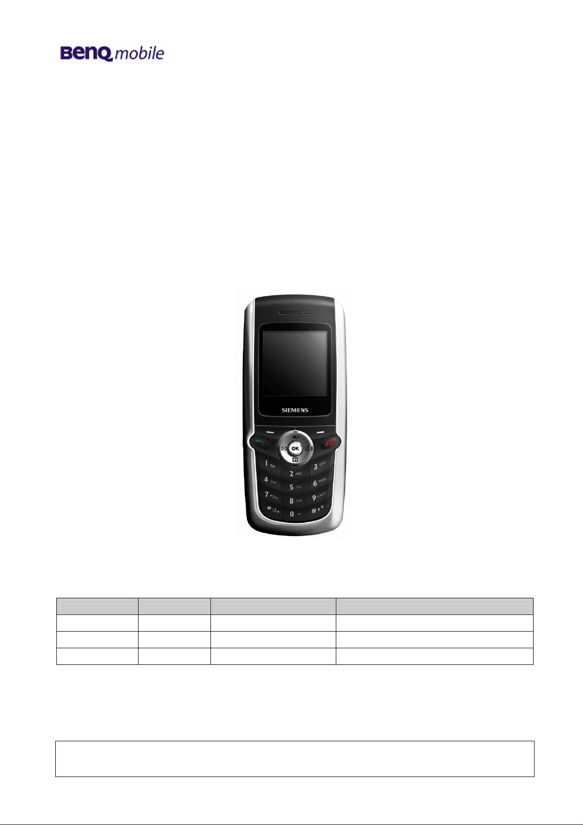
M315 / AP75
Release Date Department Notes to change
R 1.0
Technical Documentation
TD_Repair_L4 M315/AP75_R1.0.pdf Page 1 of 42
12.12.2005
BenQ Mobile (Taipei/KLF)
New document
Page 2

12/2005
Release 1.0
Table of Content
1
Introduction ...............................................................................................................................3
1.1 PURPOSE...............................................................................................................................3
1.2 SCOPE ...................................................................................................................................3
1.3 TERMS AND ABBREVIATIONS ...................................................................................................3
2 List of available level 4 (level 2,5e) parts ...............................................................................4
3 Required Software for Level 4 (level 2,5e) ..............................................................................5
4 Radio Part ..................................................................................................................................6
4.1 RECEIVER OPERATION............................................................................................................6
4.2 TRANSMITTER OPERATION......................................................................................................7
4.3 VCXO OPERATION.................................................................................................................8
4.4 BLUETOOTH OPERATION.........................................................................................................9
5 Logic ( Base-Band ).................................................................................................................10
5.1 CALYPSO-LITE......................................................................................................................12
5.2 IOTA....................................................................................................................................15
5.3 POWER SUPPLY ...................................................................................................................19
5.3.1 System power on/off Sequence ...................................................................................21
5.4 MEMORY CIRCUIT .................................................................................................................22
5.5 LCD MODULE ( LCDM).........................................................................................................24
6 Interfaces .................................................................................................................................27
6.1 AUDIO CIRCUIT .....................................................................................................................27
6.2 MELODY IC...........................................................................................................................29
6.3 AUDIO CIRCUIT .....................................................................................................................31
6.4 10 PINS I/O CONNECTOR......................................................................................................33
6.5 KEYPAD LED CIRCUIT...........................................................................................................35
6.6 VIBRATOR ............................................................................................................................36
6.7 SIM CIRCUIT ........................................................................................................................37
6.8 KEYPAD................................................................................................................................38
6.9 RTC CIRCUIT.......................................................................................................................40
7 Charging circuit.......................................................................................................................41
Technical Documentation
TD_Repair_L4 M315/AP75_R1.0.pdf Page 2 of 42
Page 3

12/2005
Release 1.0
1 Introduction
1.1 Purpose
This Service Repair Documentation is intended to carry out repairs on BenQ repair level 3-4.
1.2 Scope
This document is the reference document for all BenQ authorised Service Partners which are
released to repair Siemens mobile phones up to level 2.5.
1.3 Terms and Abbreviations
Technical Documentation
TD_Repair_L4 M315/AP75_R1.0.pdf Page 3 of 42
Page 4
12/2005
Release 1.0
2 List of available level 4 (level 2,5e) parts
(according to Component Matrix V1.xx - check C-market for updates)
Product ID Order Number Description CM
M315
M315
M315
M315
M315
M315
M315
M315
M315
M315
M315
M315
M315
M315
M315
M315
M315
M315
M315
M315
M315
M315
M315
M315
M315
M315
M315
M315
M315
M315
M315
Technical Documentation
TD_Repair_L4 M315/AP75_R1.0.pdf Page 4 of 42
Page 5

12/2005
Release 1.0
Required Equipment for Level 4 (level 2,5e)
GSM-Tester (CMU200 or 4400S incl. Options)
PC-incl. Monitor, Keyboard and Mouse
Adapter cable for Bootadapter (F30032-xx-A1)
Troubleshooting Frame M315_AP75 (F30032-xx-A1)
Power Supply
Spectrum Analyser
Active RF-Probe incl. Power Supply
Oscilloscope incl. Probe
RF-Connector (N<>SMA(f))
Power Supply Cables
Dongle (F30032-xx-A1)
BGA Soldering equipment
Reference: Equipment recommendation V1.6
(downloadable from the technical support page)
3 Required Software for Level 4 (level 2,5e)
Windows XP
XCSD Tools Level 2
GRT Version 3 or higher
Internet unblocking solution (JPICS)
Technical Documentation
TD_Repair_L4 M315/AP75_R1.0.pdf Page 5 of 42
Page 6
12/2005
Release 1.0
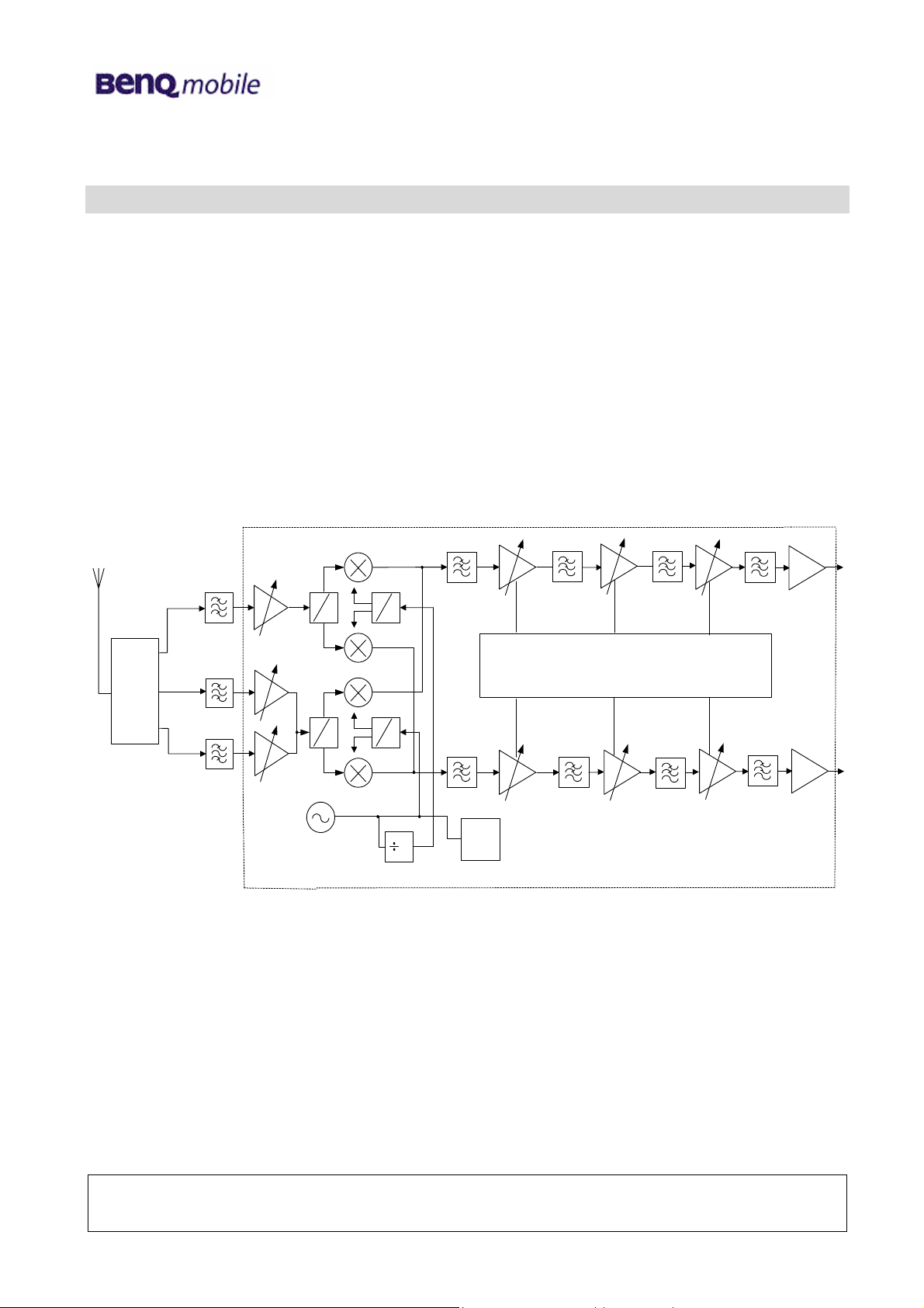
4 Radio Part
M315 / AP75 utilizes TI’s chipsets (CALYPSO-Lite and IOTA) as base-band solution. Base-band is
composed with two potions: Logic and Analog/Codec. CALYPSO-Lite is a GSM/GPRS digital baseband logic solution included microprocessor, DSP, and peripherals. IOTA is a combination of
analog/codec solution and power management which contain base-band codec, voice-band codec,
several voltage regulators and SIM level shifter etc. In addition, 56E22 integrates with other
features such as LED backlight, color LCD display, DSC, vibration, melody tone and charging etc.
The following sections will present the operation theory with circuitry and descriptions respectively.
4.1 Receiver Operation
RX GSM: 925~960 MHz
T/R
Switch
1805~1880 MHz
1930~1990 MHz
DCS:
PCS:
GSM LNA
0
90
DCS LNA
0
90
PCS LNA
RFVCO
PCS:3860~3980 MHz
DCS:3610~3760 MHz
GSM:3700~3840 MHz
0
90
Shift(1/2)
0
90
Shift(1/2)
2
GSM:
1850~1920 MHz
DCS:
1805~1880 MHz
PCS:
1930~1990 MHz
RF
Synth
ADC/DAC & Control Logic for DC Offset Cancellation
The Receiver structure in HD155155NP is a zero-IF solution. That means RF signal is directly downconverted to the baseband signal. And by the way, all of the DC-offset canceling processes
are done within chip. We do not have to care about that.
The LNA amplifies the RF signal after passing the T/R switch and RF SAW filter and before it enters
the down-converter section. The RF signal is mixed with a local oscillator (LO) signal to generate the
baseband signal.
Three LPFs are used in the baseband signal processing for reducing blocking signals. The first LPF
employs two external capacitors, and we can check whether the front-end (LNA + Mixer) is
functionally well or not by probing these two capacitors to see if there is any baseband
signal(<200kHz).
After three stages of DC-offset cancelling, the signal (I+/I-/Q+/Q-) then output to the baseband IC for
further processing.
IRxP
IRxN
QRxP
QRxN
Technical Documentation
TD_Repair_L4 M315/AP75_R1.0.pdf Page 6 of 42
Page 7
12/2005
Release 1.0
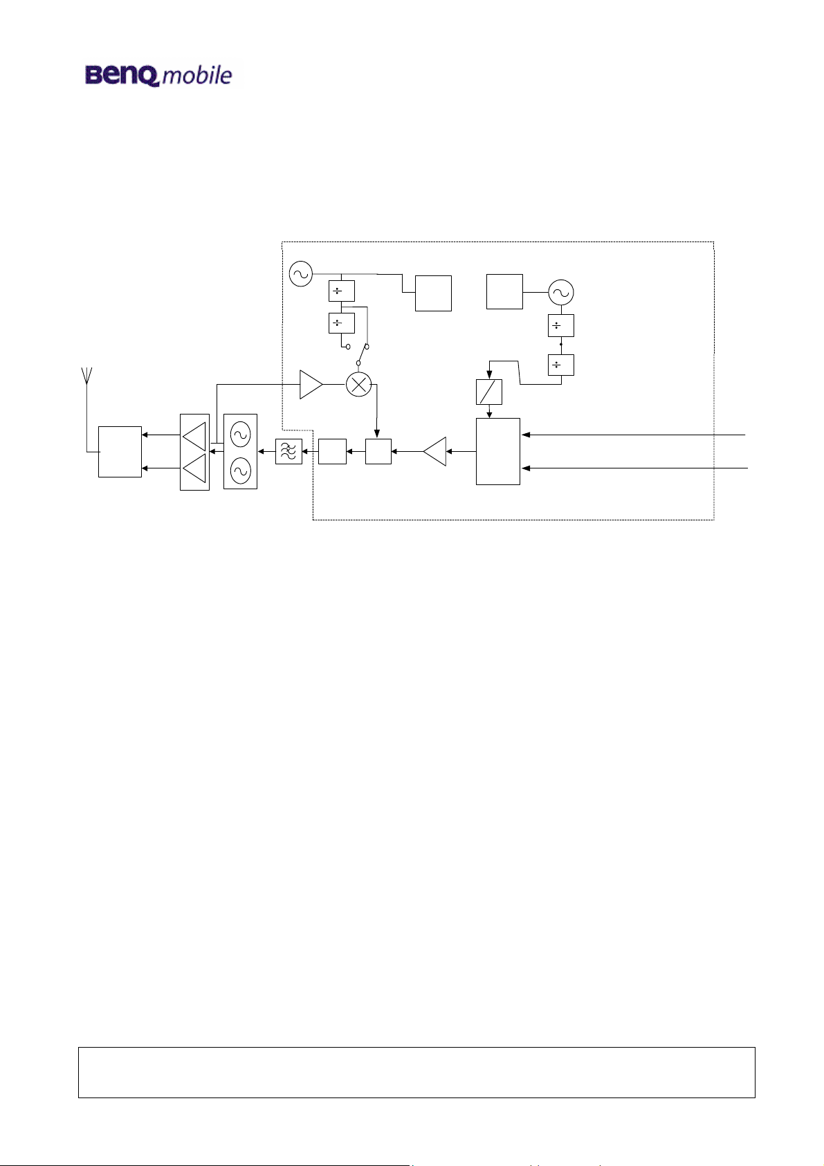
4.2 Transmitter Operation
PCS:3860~3980 MHz
DCS:3580~3730 MHz
RFVCO
T/R
Switch
Quad-Band PA
TX GSM: 880~ 915 MHz
DCS:1710~1785 MHz
PCS:1850~1910 MHz
GSM:3840~3980 MHz
GSM
GSM: 960~995 MHz
Charge
Pump
Loop Filter
2
DCS/
PCS
2
PCS:1930~1990 MHz
DCS:1790~1865 MHz
PFD
80/82 MHz
RF
Synth
Shift(1/2)
IF
Synth
0
90
I&Q Mod
IFVCO
640/656 MHz
2
2
ITxP
ITxN
QTxP
QTxN
The transmitter chain converts differential IQ baseband signals to a suitable format for
transmission by a power amplifier.
The common mode voltage range of the modulator inputs is 1.05 V to 1.45 V and they have 2.0 Vpp
differential swing. The modulator circuit uses double-balanced mixers for the I and Q paths. The
Local signals are generated by dividing the IFLO signals by 8 in GSM band and by 4 in DCS band,
and then passed to the modulator through a phase splitter / shifter. The IF signals generated are
then summed to produce a single modulated IF signal which is amplified and fed into the offset PLL
block.
Within the offset PLL block there are a down converter, a phase comparator and a VCO driver. The
down converter mixes the first local signal and the TXVCO signal to create a reference local signal
for use in the offset PLL circuit. The phase comparator and the VCO driver generate an error
current, which is proportional to the phase differential between the reference IF and the modulated
IF signals. This current is
used in a third order loop filter to generate a voltage, which in turn modulates the TXVCO.
The RF signal is then amplified by PA and power control loop to the assigned power level within the
burst ramping mask. After passing the LPF of the T/R switch, the signal is then radiated through the
antenna.
Technical Documentation
TD_Repair_L4 M315/AP75_R1.0.pdf Page 7 of 42
Page 8
12/2005
Release 1.0
4.3 VCXO Operation
+R-R
HD155155NP provides a VCXO function. With that function, we can build a reference clock
generation circuits as shown in the above graph. This means that the VCTCXO module is not
necessary for clock application, and only one crystal with 8ppm tolerance and one variocap are
enough.
The transistor in HD155155NP and two internal capacitors (C1, C2) provide a negative
resistance, and the crystal (X1) combined with some other passive components (including
variocap r : D1) to provide a positive resistance. When these two resistance values equal to each
other at some frequency, the oscillation will happen at that frequency. In our design target, the
oscillation frequency should be within 26MHz +/-15 ppm.
Technical Documentation
TD_Repair_L4 M315/AP75_R1.0.pdf Page 8 of 42
Page 9
12/2005
Release 1.0
4.4 Bluetooth Operation
26MHz
B5E-VCXO
VBAT
LDO
2.8V
CLK_S E L
OR
Gate
TCXOEN
2402~2480 MHz
IRDA
UART
B C 3-Handphone
G2-lite
MCSI
SPI Int erface
The Bluetooth main chip – BC3-Handphone deals with BT RF signal from chip antenna and
baseband signal from G2-lite including down/up-converting, de/- modulation and de/- coding … The
BC3-Handphone could accept clock frequency from 8MHz to 40MHz. In our application, we feed the
chip with 26MHz clock from RF chip, HD155155N, and share with G2-lite by an OR-Gate. So GSM
part and BT part could go to sleep respectively. BC3-Handphone could wake G2-lite up by a
interrupt. The BC3-Handphone is controlled by AT commands that come from G2-lite via IRDA
UART. The Data between BC3-Handphone and G2-lite are transmitted and received via MCSI
interface. The SPI interface is reserved for firmware downloading for BT chip of Flash-type. The
power BT chip needed outside is 2.8V the same with voltage level of I/O interface of G2-lite.
INTE RRUPT
Technical Documentation
TD_Repair_L4 M315/AP75_R1.0.pdf Page 9 of 42
Page 10

12/2005
Release 1.0
5 Logic ( Base-Band )
Introduction:
56E22 utilizes TI’s chipsets (CALYPSO-Lite and IOTA) as base-band solution. Base-band is
composed with two potions: Logic and Analog/Codec. CALYPSO-Lite is a GSM/GPRS digital
base-band logic solution included microprocessor, DSP, and peripherals. IOTA is a combination
of analog/codec solution and power management which contain base-band codec, voice-band
codec, several voltage regulators and SIM level shifter etc. In addition, 56E30 integrates with
other features such as LED backlight, color LCD display , DSC, vibration, melody tone and
charging etc. The following sections will present the operation theory with circuitry and
descriptions respectively.
Block Diagram CPU CALYPSO (HERCROM40 )
Technical Documentation
TD_Repair_L4 M315/AP75_R1.0.pdf Page 10 of 42
Page 11
12/2005
Release 1.0
IOTA
Technical Documentation
TD_Repair_L4 M315/AP75_R1.0.pdf Page 11 of 42
Page 12

12/2005
Release 1.0
5.1 Calypso-Lite
CALYPSO-Lite (HERCROM400) is a chip implementing the digital base-band processor of a
GSM/GPRS mobile phone. This chip combines a DSP sub-chip (LEAD2 CPU) with its program
and data memories, a Micro-Controller core with emulation facilities (ARM7TDMIE) and an
internal 2M-bit RAM memory, a clock squarer cell, several compiled single-port or 2-ports RAM
and CMOS gates.
Major functions of this chip are as follows:
Real Time Clock (RTC)
The RTC block is an embedded RTC module fed with an external 32.768KHz Crystal. Its basic
functions are:
1. Time information (seconds/minutes/hours)
2. Calendar information (Day/Month/Year/ Day of the week) up to year 2099
3. Alarm function with interrupts (RTCINT is generated to wake up ABB)
4. 32KHz oscillator frequency gauging
Pulse Width Light (PWL)
This module allows the control of the backlight of LCD and keypad by employing a 4096 bit
random sequence .In the 56E30, we use the LT/PWL function to turn on the keypad light LED.
MODEM-UART
This UART interface is compatible with the NS 16C750 device which is devoted to the
connection to a MODEM through a standard wired interface. The module integrates two 64
words (9 and 11 bits) receive and transmit FIFOs which trigger levels are programmable. All
modem operations are controllable either via a software interface or using hardware flow control
signals. In 56E30 , we implement software flow control by only two signals: TXD0 and RXD0.
General Purposes I/O (GPIO)
Calypso-Lite provides 16 GPIOs configurable in read or write mode by internal registers. In
56E30, we utilize 9 of them as follows , others are used in the dual function mode or N/A:
IO 0 : SPK_FM_HF
IO 1 : VOL_CLK
IO 2 : MELODY_INT
IO 3 : VOL_UpDown
IO 4 : FM_SPK
Technical Documentation
TD_Repair_L4 M315/AP75_R1.0.pdf Page 12 of 42
Page 13

12/2005
Release 1.0
IO 5 : X
IO 6 : ACCESSORY_IN
IO 7 : NRESET_OUT
IO 8 :
IO 9 : NLED_DRIVE_SD
IO 10 : FM_EN
IO 11 : FM_SCL
IO 12 : FM_SDA
IO 13 :
IO14: SRAM high-byte enable
IO15: SRAM low-byte enable
Serial Port Interface (SPI)
The SPI is a full-duplex serial port configurable from 1 to 32 bits and provides 3 enable signals
programmable either as positive or negative edge or level sensitive. This interface is working on
13MHz and is used for the GSM/GPRS baseband and voice A/D, D/A with IOTA
Memory Interface and internal Static RAM
For external memory device (Flash and SRAM), this interface performs read and write access
with adaptation to the memory width. It also provides 6 chip-select signals corresponding each
to an address range of 8 mega bytes. One of these chip-select is dedicated to the selection of
an internal memory. In 56E30, we employ nCS0 (NROM_CS0) for external 64 Mbits Flash and
nCS1 (NRAM_CS1) for external 16Mbits SRAM. A 2Mbit SRAM is embedded on the die and
memory mapped on the chip-select nCS6 of the memory interface .The access cycle is
guaranteed with 0 wait-state for any cycle frequency up to 39MHz. About others chip selects
allocation are nCS2 (NDSCM_CS2) for DSC backend IC and nCS3 (NLCDM_CS3) for LCDM
driver and nCS4 for melody IC ..
SIM Interface
The Subscriber Identity Module interface will be fully compliant with the GSM 11.11 and ISO/IEC
7816-3 standards. Its external interface is 3 Volts only. 5 Volts adaptation will be based on
external level shifters.
JTAG
In 56E30, JTAG is used for software debugging.
Technical Documentation
TD_Repair_L4 M315/AP75_R1.0.pdf Page 13 of 42
Page 14

12/2005
Release 1.0
Time Serial Port (TSP)
The TPU is a real-time sequencer dedicated to the monitoring of GSM/GPRS baseband
processing. The TSP is a peripheral of the TPU which includes both a serial port (32 bits) and a
parallel interface. The serial port can be programmed by the TPU with a time accuracy of the
quarter of GSM bit. The serial port is uni-directional (transmit only) when used with IOTA. The
serial port provides 4 enable signals programmable either as positive or negative edge or level
sensitive. This serial port is derived from 6.5MHz and used to control the real time GSM windows
for the baseband codec and the windows for ADC conversion.
TSP Parallel interface (ACT)
The parallel interface allows control 13 external individual outputs and 1 internal signal with a
time accuracy of the quarter of GSM bit. These parallel signals are mainly used to control the RF
activity. In 56F05, we employ 5 of them to control RF activity.
TSPACT1: GSM_T/R
TSPACT2: DCS_T/R
TSPACT3: PCS_RX
TSPACT6: TX_ON
TSPACT9: Band Select
TSPACT10: Latch enable
Radio Interface (RIF)
The RIF (Radio Interface) Module is a buffered serial port derived from the BSP peripheral
module of the defined for TMS320C5X. The external serial data transmission is supported by a
full-duplex double-buffered serial port interface. The interface is used for transfer of baseband
transmit and receive data and also to access all internal programmation registers of the device.
Miscellaneous:
Some important Baseband /RF interface signals are defined as follows:
CLKTCXO: 13MHz VTCXO Clock from RF circuit
TCXOEN: 13MHz VTCXO Clock Enable signal
Technical Documentation
TD_Repair_L4 M315/AP75_R1.0.pdf Page 14 of 42
Page 15

12/2005
Release 1.0
5.2 IOTA
Together with a digital base-band device (Calypso-Lite), IOTA is part of a TI DSP solution
intended for digital cellular telephone applications including GSM 900, DCS 1800 and PCS 1900
standards (dual band capability).
It includes a complete set of base-band functions to perform the interface and processing of voice
signals, base-band in-phase (I) and quadrature (Q) signals which support single-slot and multislot mode, associated auxiliary RF control features, supply voltage regulation, battery charging
control and switch ON/OFF system analysis. IOTA interfaces with the digital base-band device
through a set of digital interfaces dedicated to the main functions of Calypso-Lite, a base-band
serial port (BSP) and a voice-band serial port (VSP) to communicate with the DSP core (LEAD),
a micro-controller serial port to communicate with the micro-controller core and a time serial port
(TSP) to communicate with the time processing unit (TPU) for real time control.
IOTA also includes on chip voltage reference, under voltage detection and power-on reset
circuits.
Major functions of this chip are as follows:
Baseband Codec (BBC)
The baseband codec includes a two-channel uplink path and a two-channel downlink path.
The baseband uplink path (BUL) modulates the bursts of data coming from the DSP via the
baseband serial port (BSP) and to be transmitted at the antenna. Modulation is performed by a
GMSK modulator. The GMSK modulator implemented in digital technique generates In-phase (I)
and Quadrature (Q) components, which are converted into analog base-band by two 10 bits
DACs filters. It also includes secondary functions such as DC offset calibration and I/Q gain
unbalance.
The baseband downlink path (BDL) converts the baseband analog I & Q components coming
from the RF receiver into digital samples and filters these resulting signals through a digital FIR
to isolate the desired data from the adjacent channels. During reception of burst I & Q digital
data are sent to the DSP via the baseband serial port (BSP) at a rate of 270 KHz.
Automatic Frequency control (AFC)
The automatic frequency control function consists of a digital to analog converter optimized for
high resolution DC conversion. Its purpose is to control the frequency of the GSM 13MHz
oscillator to maintain mobile synchronization on the base station and allow proper transmission
and demodulation.
Technical Documentation
TD_Repair_L4 M315/AP75_R1.0.pdf Page 15 of 42
Page 16

12/2005
Release 1.0
Automatic Power Control (APC)
Purpose of the Automatic Power Control (APC) is to generate an envelope signal to control the
power ramping up, ramping down and power level of the radio burst.
The APC structure is intended to support single slot and multi-slots transmission with smooth
power transition when consecutive bursts are transmitted at different power level. It includes a
DAC and a RAM in which the shape of the edges (ramp-up and ramp-down) of the envelope
signals are stored digitally. This envelope signal is converted to analog by a 10 bits digital to
analog converter. Timing of the APC is generated internally and depends of the real time signals
coming from the TSP and the content of two registers which control the relative position of the
envelope signal versus the modulated I & Q.
Time serial port (TSP)
Purpose of the time serial port is to control in real time the radio activation windows of IOTA
which are BUL power-on, BUL calibration, BUL transmit, BDL power-on, BDL calibration and BDL
receive and the ADC conversion start.
These real time control signals are processed by the TPU of DBB and transmitted serially to
ABB via the TSP, which consists in a very simple two pins serial port. One pin is an enable
(TEN) the other one the data receive (TDR). The master clock CK13M divided by 2 (6.5MHz) is
used as clock for this serial port.
Voice band Codec (VBC)
The VBC processes analog audio components in the uplink path and transmits this signal to DSP
speech coder through the voice serial port (VSP). In the downlink path the VBC converts the
digital samples of speech data received from the DSP via the voice serial port into analog audio
signal. Additional functions such as programmable gain, volume control and side-tone are
performed into the voice band codec.
Micro-controller serial port (USP)
The micro-controller serial port is a standard synchronous serial port. It consists in three
terminals, data transmit (UDX), data receive (UDR) and port enable (UEN). The clock signal is
13MHz clock. The USP receives and sends data in serial mode from and to the external microcontroller and in parallel mode from and to the internal GSM Baseband a Voice A/D D/A
modules. The micro-controller serial port allow read and write access of all internal registers
under the arbitration of the internal bus controller.
Technical Documentation
TD_Repair_L4 M315/AP75_R1.0.pdf Page 16 of 42
Page 17

12/2005
Release 1.0
SIM card shifters (SIMS)
The SIM card digital interface in ABB insures the translation of logic levels between DBB and SIM
card, for transmission of 3 different signals; a clock derived from a clock elaborated in DBB, to the
SIM card (DBBSCKSIMCLK). a reset signal from DBB to the SIM card (DBBSRSTSIMRST),
and serial data from DBB to SIM card (DBBSIOSIMIO) and vice-vera.
The SIM card interface can be programmed to drive a 1.8V and 3 V SIM card
Voltage Regulation (VREG)
Linear regulation is performed by several low dropout (LDO) regulators to supply analog and
digital baseband circuits.
(1) LDO VRDBB generates the supply voltage (1.85V, 1.5V,and 1.35V) for the digital core of
DBB. In 56E30, it is programmed to 1.5V. This regulator takes power from the battery
voltage
(2) LDO VRABB generates the supply voltage 2.8V for the analog function of ABB. It is
supplied by the battery.
(3) LDO VRIO generates the supply voltage 2.8V for the digital core of ABB and digital I/O’s of
DBB and ABB. It is supplied from battery voltage.
(4) LDO VRMEM generates the supply voltages 2.8V for DBB memory interfaces I/O’s.
(5) LDO VRRAM generates the supply voltages 2.8V for DBB memory interfaces I/O’s
(6) LDO VRRTC generates the supply voltages (1.85,1.5, or 1.35V) and supply voltage 1.5V for
the following block of DBB (real time clock and 32K oscillator ). It’s supplied by UPR
(7) LDO VRSIM generates the supply voltages (1.8V, 2.9V) for SIM card interface I/O’s
Baseband Serial Port (BSP)
The BSP serial interface is used for both configuration of the GSM baseband and voice A/D D/A
(read and write operation in the internal registers), and transmission of the radio data to the DSP
during reception of a burst by the downlink part of the GSM baseband & voice A/D D/A. Four
pins are used by the serial port: BFSR and BDR for receive, BFSX and BDX for transmit. BDX is
the transmitted serial data output. BFSX is the transmit frame synchronization and is used to
initiate the transfer of the transmit data. BDR is the received serial input. BFSR is the receive
frame synchronization and is used to initiate the reception data.
Technical Documentation
TD_Repair_L4 M315/AP75_R1.0.pdf Page 17 of 42
Page 18

12/2005
Release 1.0
Battery charger Interface (BCI)
The main function of the ABB charger interface is the charging control of either a 1-cell Li-ion
Battery or 3-serie Ni-MH cell batteries with the support of the micro-controller. The battery
monitoring uses the 10 bit ADC converter from the MADC to measure the battery voltage, battery
temperature, battery type, battery charge current, battery charger input voltage. The magnitude
of the charging current is set by the 10 bits of a programming register converted by an 10 bit
Digital to Analog Converter, whose output sets the reference input of the charging current control
loop. The battery charger interface performs also some auxiliary functions. They are battery precharge, battery trickle charge and back-up battery charge if it is rechargeable.
Monitoring ADC (MADC)
The MADC consists in a 10-bit analog to digital converter combined with a nine inputs analog
multiplexer. Out of the nine inputs five are available externally, the four remaining being
dedicated to main battery voltage, back up battery voltage, charger voltage and charger current
monitoring. On the five available externally three are standard inputs intended for battery
temperature, battery type measurements.
Reference Voltage / Power on Control (VRPC)
An integrated band-gap generates a reference voltage. This reference is available on an external
pin for external filtering purpose only. This filtered reference is internally used for analog
functions. The external resistor connected between pin IBIAS and GNDREF sets, from the bandgap voltage, the value of the bias currents of the analog functions. The VRPC block is in charge
to control the Power ON, Power OFF, Switch On, and Switch OFF sequences. Even in Switch
OFF state some blocks functions are performed. These “permanent” functions are functions,
which insure the wake-up of the mobile such as ON/OFF button detection or charger detection.
Interrupts are generated at power-down detection of the PWON button and when abnormal
voltage conditions are detected.
Internal bus and interrupt controller (IBIC)
Read and write access to all internal registers being possible via both the BSP and USP,
purpose of the internal bus controller is to arbitrate the access on the internal bus and to direct
the read data to the proper serial port. During reception of a burst the internal bus controller
assign the transmit part of the BSP to the base-band downlink to transfer the I & Q samples to
the DSP.
This block also handles the internal interrupts generated by the MADC, BCI and VRPC blocks
and generates the micro-controller interrupt signal INT2.
Technical Documentation
TD_Repair_L4 M315/AP75_R1.0.pdf Page 18 of 42
Page 19

12/2005
Release 1.0
5.3 Power Supply
VBAT
VCAM
VCMEM
VLMEN
VCDBB
VCIO1
VCIO2
VCABB
VBAT
ABB
RSIM
1.8/2.9V
10mA
RRAM
1.8/2.8
50mA
RMEM
1.8/2.8V
60mA
RDBB
1.3/1.5/1.8V
120mA
RIO
2.8V
100mA
ABB
D Igital
Core
I/O
VRSIM
VRRAM
VRMEM
VSDBB
VRDBB
VRIO1
VRIO2
SIM
CARD
SRA M
CORE
M enory
IO
CORE
DBB
Memories
I/O
DBB
COre
DBB
I/O
BACK
UP
Technical Documentation
BBS
ABB
VRPC Core
ABB
Analog
Core
RABB
2.8V
50mA
RSIM
1.8/2.9V
10mA
VLRTC
VRABB
Sel 1.8V
VRRTC
D BB S plit P o w er
Low Power Domain
Sel 1.5V
DBB Backup
RTC
I/O R T C
TD_Repair_L4 M315/AP75_R1.0.pdf Page 19 of 42
Page 20

12/2005
Release 1.0
Description:
The voltage regulators embedded in IOTA consists of seven sub blocks. Several low-dropout (LDO)
regulators perform linear voltage regulation. These regulators supply power to internal analog and
digital circuit, to DBB processor, and to external memory.
· LDO (VRDBB) is a programmable regulator that generates the supply voltages(1.8V,1.5V and
1.3V) for the core of the DBB processor. The main battery supplies VRDBB.
· LDO (VRIO) generate the supply voltage (2.8V) for the digital core and I/O of the TWL3014 device.
The main battery supplies VRIO.
· LDO (VRMEM) is a programmable regulator that generates the supply voltages (2.8V and 1.8V) for
external memories (typically flash memories) and DBB memory interface I/O. The main battery
supplies VRMEM.
· LDO (VRRAM) is a programmable regulator that generate the supply voltages (2.8V and 1.8V) the
external memory (typically SRAM memories) and DBB memory interface I/Os. The main battery
supplies VRRAM.
· LDO (VRABB) generates the supply voltage (2.8V) for the analog functions of the TWL 3014
devices. The main battery supplies VRABB.
· LDO (VRSIM) is a programmable regulator that generates the supply voltages (2.9V and 1.8V) SIM
card and SIM card devices. The main battery supplies VRSIM.
· LDO (VRTC) is a programmable regulator that generate the supply voltage (1.8V.1.5Vand 1.3V) for
real time clock and the 32-KHZ oscillator located in the DBB device during all modes. The main or
backup battery supplies VRTC.
Technical Documentation
TD_Repair_L4 M315/AP75_R1.0.pdf Page 20 of 42
Page 21

12/2005
Release 1.0
5.3.1 System power on/off Sequence
Power on mode
On the plug-in of the valid main battery or backup battery, an internal reset is generated (POR).
After a power-on sequence, the TWL3014 device is in the BACKUP or OFF state.
When these conditions occur in the power on state, the hardware power on sequence starts:
1. Enable band-gap (VREF and IREF)
2. Check if Main Battery voltage is greater than 3.2V
3. Enable charge VRDBB-VRABB-VRMEM-VRRAM
4. Regulator OK.
5. ON_nOFF=1, ABB RSTz=1
6. NRESET pin is set from ‘L’ to ‘H’
7. 13MHz clock oscillator is enabled
Power off mode
This state is reached when there is not enough voltage in the main battery and backup battery or
when both batteries are disconnected.
1. Send INT1
2. Start 5*T watchdog Timer , T= 32K period
3. ON_nOFF=0
4. ABB RSTz=0
5. Disable the LDO’s using MSKOFF content and the band-gap
6. “MBATLOW”=0
Technical Documentation
TD_Repair_L4 M315/AP75_R1.0.pdf Page 21 of 42
Page 22

12/2005
Release 1.0
5.4 Memory circuit
Block diagram
CLK
ADV#
WP#
RST#
OE#1
CE#1
VCC1
A[MAX:0]
Flash Die #1
28F640W18
WE#
VPP
VCCQ
WAIT
D[15:0]
S-VCC/P-VCC
P-CS#/S-CS#
S-CS2
S-OE#/P-OE#
RAM Die
4,8,16-Mbit SRAM
S-WE#/P-WE#
P_MODE
R_UB#
R_LB#
Description:
The two diagrams show the memory circuit of 56F05 and internal package connections for the
Stacked CSP family with multiple die. The 64-Mbit 1.8 Volt Intel Wireless Flash Memory Stacked
CSP Family encompass multiple flash memory + 16M bit RAM die combinations.
Technical Documentation
TD_Repair_L4 M315/AP75_R1.0.pdf Page 22 of 42
Page 23

12/2005
Release 1.0
Schematic
VRME M
FDP2
VBAT
C204
2.8V
VRRAM
C200
1uF
BGND
1uF
BGND
74.03218.03B
74.08878.B3B
U202
1
VIN
2
GND
3 4
ON/OFF
AAT3218IGV-1.8
BGND
VRMEM
BGND
VOUT
NOISE
C201
0.1uF
1.8V
5
BGND
2.8V
C203
0.01uF
BGND
1.8V
R202
C206
0.1uF
BGND
1K
PMODE
A[1..22]2,6,7,9
C205
1uF
R201
Address line
A22
A21
A20
A19
A18
A17
A16
A15
A14
A13
A12
A11
A10
A9
A8
A7
A6
A5
A4
A3
A2
A1
VRMEM
VRRAM
1.8V
47K
WP#
C202
0.1uF
BGND
U203
E3
A25
D3
A24
C3
A23
C7
A22
B7
A21
E6
A20
B3
A19
B2
A18
D2
A17
F8
A16
E8
A15
F7
A14
D8
A13
C8
A12
B8
A11
E7
A10
D7
A9
F6
A8
E2
A7
F2
A6
C1
A5
B1
A4
D1
A3
E1
A2
F1
A1
G1
A0
J8
VCCQ(I/O)
K7
VCCQ(I/O)
L3
VCCQ(I/O)
K4
S-VCC(SRAM)
K5
P-VCC(PSRAM)
B5
VCC1
L4
VCC1
K6
VCC2
B6
VCC2
D4
VPP
E4
WP#
K8
P-Mode
F4
RST#
RD38F2030W0ZBQ0CSP88
72.38203.A0T
64Mb Flash + 16Mb P SRAM
S-CS1#
ADV#
WAIT
CE1#
CE2#
S-CS2
P-CS#
OE1#
OE2#
R-OE#
R-UB#
R-LB#
WE#
R-WE#
GND
GND
GND
GND
GND
GND
GND
GND
D15
D14
D13
D12
D11
D10
CLK
3.3 V<VBAT<4.2V
Data bus
J7
D15
H6
D14
G6
D13
H5
D12
J4
D11
G4
D10
J3
G2
H7
J6
G5
J5
H4
G3
H3
H2
C6
E5
G7
2.8V
K1
G8
J1
C5
D6
J2
H8
H1
F3
C2
F5
D5
L1
L2
L5
L7
C4
B4
L8
L6
BGND
D9
D8
D7
D6
D5
D4
D3
D2
D1
D0
D9
D8
D7
D6
D5
D4
D3
D2
D1
D0
Intel 80 series control
D[0.. 15] 2,6,7,9
NROM_CS0 2
NRAM_CS1 2
VRMEM
R200
47K
VRRAM
NFOE 2,6,7,9
NBHE 2
NBLE 2
RNW 2,6,7,9
Technical Documentation
TD_Repair_L4 M315/AP75_R1.0.pdf Page 23 of 42
Page 24

12/2005
Release 1.0
5.5 LCD module ( LCDM)
Connector between PCBA and LCDM
RN103
LFA144
O4
I4
9
O3
I3
8
O2
I2
O1I1
D
D
N
N
G
G
21
2 1
D
D
N
N
3 7
G
G
O1 I1
4
O2
I2
5
O3
I3
6
O4
I4
RN104
LFA144
RN105
LFA144
10
I4
9
I3
8
I2
D
N
G
RN106
LFA144
10
I4
9
I3
8
I2
D
N
G
21
6
5
4
37
J325
DB15
8
9
10
6
O4
5
O3
4
O2
37
O1I1
D
N
G
21
6
O4
5
O3
4
O2
37
O1I1
D
N
G
BGND
1
DB15
2
DB14
DB13
3
DB13
DB12
4
DB12
5
DB11
DB10
6
DB10
DB9
7
DB9
8
DB8
DB8
DB7
9
DB7
DB6
10
DB6
DB5
11
DB5
DB4
12
DB4
DB3
13
DB3
DB2
14
DB2
DB1
15 16
DB1 DB0
CSTN LCDM Connector
short jump
LED2+(A)
LED2-(K)
LED1+(A)
LED1-(K)
HW_ID
/RESET
GND
VCC
F(/WR)
RW(/RD)
SJ329
1
2
30
29
28
27
26
/RESET
25
24
IM1
23
IM2
22
21
20
/CS
19
RS
RS
18
17
DB0D1
DNI 0.1uF
VRIO
R329
SJ326
0
LED_OUT
short jump
SJ325
short jump
12
LED_IN
12
NLCDM_CS3
A1
C328
2
1uF
1
OJ328
12
open jump
/CS
/WR
/RD
2
C332
1
BGND
10
D[0..15]
2,7,8
D15
D14 DB14
D13
D12
D11 DB11
D10
D9
D8
D7
D6
D5
D4
D3
D2
D0
LCDM_HW_ID
NRSTOUT/IO7
A[1.. 22]
RNW
NFOE
LCDM_HW_ID ( ADIN1 ) voltage allocation vs LCDM vendor : (we use the ADIN1 (Iota) to
detect the LCDM vendor)
272, /* LCDM_Nanya : 0.0 ~ 0.272V */
410, /* Reserve : 0.273 ~ 0.410V */
616, /* Reserve : 0.411 ~ 0.616V */
926, /* Reserve : 0.617 ~ 0.926V */
1390, /* LCDM_GiantPlus : 0.927 ~ 1.390V */
1718, /* Reserve : 1.391 ~ 1.718V */
Technical Documentation
TD_Repair_L4 M315/AP75_R1.0.pdf Page 24 of 42
Page 25

12/2005
Release 1.0
LCM mechanical outline
Description
This display module is a transmissive color STN (CSTN) Liquid crystal display (LCD) module of
glass construction with a black background. The display has an internal transflector. The display
consists of 128 ( xRGB Stripe) x 128 pixel with 65K colors. bar connections to a flex foil
accommodating components to drivers and the backlighting system. The backlighting system will
consist of one light guide illumination both cells with a white backlight. Interconnection to the main
board will be by a board to board connector.
This display module consists of:
CSTN Cell with polarizers, COG
Enhancement films (DBEF + 2*BREF)
Mechanical support/carrier system with Magnesium frame
One illumination system with 2 White LED’s.
Flexfoil with SMD component (include board to board connector for connection to the main part
of the phone and between the module)
Technical Documentation
TD_Repair_L4 M315/AP75_R1.0.pdf Page 25 of 42
Page 26

12/2005
Release 1.0
White LED driver schematic
VBAT
BL325
BEAD(0603)
NLED_DRIVE_SD/IO9
BGND
C325
1uF(0603)
1
2
BGND
2
R331
47K
1
C327
2
1
1uF (0603)
L325
33uH
U325
1
OVP
2
VIN
3
EN
4
AGND NC
MIC 2287 WHITE LED DRIVER
PGND
SW
8
7
6
FB
5
BGND
Max 20mA
1
D325
RB520S-30
2
BGND
C326
2
1uF (0603)
1
R327
2
R328
82K
4.7K
1
2
R326
3.9
1
BGND
DAC
1
2
C
2
1
C333
LED_OUT
DAC range 0~1023 step
LED_IN
Technical Documentation
TD_Repair_L4 M315/AP75_R1.0.pdf Page 26 of 42
Page 27

12/2005
A
y
A1A
K
K
Release 1.0
6 Interfaces
6.1 Audio circuit
3.7.1 Uplink path
MICBIAS
-10dBm0
MICIP
-10dBm0
MICIN
R172
R173
2.0V
1
1K
R164
1
C160
0.1UF
C165 0.1UF
C168
DNI
R163
1K
EMI
rra
1
2
C169
4.7uF(0603)
R162 1K
3
68ohm
47pF
B2
TP150
EN150
C1
C3
TP151
1
1
MICROPHONE_0
1
1
.
.
T151
.
.
DNI
2
2
T150
DNI
3
4
X150
Technical Documentation
BGND
BGND
BGND
TD_Repair_L4 M315/AP75_R1.0.pdf Page 27 of 42
Page 28

12/2005
Release 1.0
Downlink path
EARN-
RECEVER_N 9
EARP+
Iota part
RECEVER_N
RECEVER_P
TP400
1
C181
27PF
TP401
BGND
1
C182
27PF
BGND
SJ402
SJ403
12
short jump
12
short jump
RECEVER_P
..
T400
TVS
12
..
T401
TVS
12
9
RECEIVERRECEIVER+
LS1
Receiver
BGND
Description
The audio circuit is divided into two parts, uplink and downlink path.
For uplink path, the analog voice signals are fed into IOTA from the microphone differential input
and then transmitted to G2 DSP via the voice-band series port (VSP). After being modulated, the
signals go through the uplink I/Q path to the RF transceiver and transmitted from the antenna.
The microphone circuit is biased from MICBIAS of IOTA. The bias circuit, R163, R164, R162 mainly
provides the optimal operation point for the microphone signals, MICP and MICN. For downlink path,
the signals received from the antenna are down-converted to I/Q signals and then transmitted to G2
DSP. After being demodulated, the signals are fed to IOTA via voice-band interface and then
amplified to drive the receiver in the EARP and EARN .
Technical Documentation
TD_Repair_L4 M315/AP75_R1.0.pdf Page 28 of 42
Page 29

12/2005
Release 1.0
6.2 Melody IC
Schematic
A[1.. 22]2
Yamaha 16 tone melody
IC
D[0..15]2,4,9
RNW2
NMELODY_CS4
A1
VRIO
2
NFOE2
1 2
NMELODY_INT/IO22
LOUD_SPK_P 9
16
15
14
13
12
11
10
LOUD_SPK_N 9
VBAT
2
1
C405
0.1uF
12
VRIO
2
IO4/F M_SPK
Gain = R404 / R403
f1 = 1 / (2pi * R403 * C404)
f2 = 1 / (2pi * R404 * C407)
C406
4.7uF
C404
0.1uF
1
OJ400
open jump
C408
2
0.1uF
2
1
1 2
R403
20K
1 2
R406
20K
VRIO
C407
270pF
U401
4
A
5
Vcc
6
S
NC7SB3157
2
1
L- B0-A
R404
62K
3
B0
2
Gnd
BGND
1
B1
FM_AUDIO_LEFT
D7
D6
D5
D4
D3
D2
D1
D0
5
U400
2
26
D1
27
D0
28
/WR
29
/CS
30
A0
31
/RD
32
SDOUT
R4050
13MOUT3
NRSTOUT/IO72
K
C
1 234
TPL400
1
L
1
T
X
E
1
YMU759
T
Q
S
R
I
R
/
/
D6D5D4D3D
L
E
S
F
I
5 678 9
0
0
4
C
1
0
4
R
C
L
L
P
2
F
n
1
1
2
2
k
1
3
.
3
1
BGND
17181920212223242
1
2
2D7
T
T
T
X
U
U
E
O
O
P
P
S
S
SPVSS
SPVDD
HPOUT-R
HPOUT-L/MONO
F
D
E
S
S
D
R
V
V
V
BGND
F
u
7
.
4
1
0
4
C
EQ3
EQ2
EQ1
H- B1-A
FM
Technical Documentation
TD_Repair_L4 M315/AP75_R1.0.pdf Page 29 of 42
Page 30

12/2005
Release 1.0
Description:
The Yamaha Melody IC (YMU759 MA2) mainly generate multi-tone for speaker. The main features
are
1. Equipped with FM generator function and ADPCM playback function
3. Number of voice simultaneously generated
4. When only 2-operator tone are used : up to 16 voices can be generated simultaneously
5. When only 4-operator tone are used : up to 8 voices can be generated simultaneously
6. Built-in 4-bit 1ch ADPCM decoder, and supports two kinds of sampling frequency , 4kHz and
8kHz.
7. Built-in output 550mW (AVDD=3.6V) speaker amplifier
8. Built-in hardware sequencer
9. Built-in circuit for sound quality correcting equalizer
10. Supports stereophonic D/A converter
11. Provided with a stereophonic analog output terminal for headphone
12. 4 wire serial interface or 12 wire parallel interface can be selected
13. PLL is built-in to support master clock in 2MHz to 20MHz range
14. Support power down mode(Typical current: 1uA or less)
15. Power supply is divided into analog power supply for speaker amplifier and power supply for the
others
Analog power supply for speaker amplifer (SPVDD): 2.7V~4.5V (Typ 3.6V)
Digital power supply for the others (VDD):2.7V~3.3V(Typ 3.0V)
Besides, IO4 control analog switch U401 to decide FM output to headset or Loud speaker.
Technical Documentation
TD_Repair_L4 M315/AP75_R1.0.pdf Page 30 of 42
Page 31

12/2005
Release 1.0
6.3 Audio circuit
Uplink path
-10dBm0
MICIP 2
-10dBm0
MICIN 2
2.0V
MICBIAS2
R155 1K
R159 1K
Downlink path
BGND
C153
0.1uF
C154
0.1uF
R152 1K
BGND
C172
C
C170
C
C171
C
C158
0.1uF
BGND
R154
R153
1K
C159
4.7uF(0603)
1K
C160
27pF
Close to
MIC
U162
C3
C1
I3O3
GND
I1
O1
CSPEMI202A
For PCBA
A3
B2
A1
BGN
D
T150
TVS
SEND_END_KEY
TP158
1
X2
1
1
2
2
3
3
2
2
T151
..
..
TVS
1
1
BGND
4
5
6
456
Microphone
BGND
TP159
1
RC-
RC+
C430
39pF
2
C431
39pF
1
2
1
BGND
Iota part
Technical Documentation
TD_Repair_L4 M315/AP75_R1.0.pdf Page 31 of 42
Page 32

12/2005
Release 1.0
RC-
BL400 BLM15AG102SN1
LS1
Receiver
RC+
BL401 BLM15AG102SN1
2
C414
10pF
1
BGND
2
C412
100pF
1
2
C413
10pF
1
RECEIVER-
RECEIVER+
1
..
T400
TVS
2
1
2
..
T401
TVS
Description
The audio circuit is divided into two parts, uplink and downlink path.
For uplink path, the analog voice signals are fed into IOTA from the microphone differential input
and then transmitted to G2 DSP via the voice-band series port (VSP). After being modulated, the
signals go through the uplink I/Q path to the RF transceiver and transmitted from the antenna.
The microphone circuit is biased from MICBIAS of IOTA. The bias circuit provides the optimal
operation point for the microphone signals, MICP and MICN. For downlink path, the signals received
from the antenna are down-converted to I/Q signals and then transmitted to G2 DSP. After being
demodulated, the signals are fed to IOTA via voice-band interface and then amplified to drive the
receiver in the EARP and EARN.
Technical Documentation
TD_Repair_L4 M315/AP75_R1.0.pdf Page 32 of 42
Page 33

12/2005
Release 1.0
6.4 10 Pins I/O connector
Schematic
BGND
20.N2003.010
J450
1
12
2
3
4
5
6
7
8
9
1011
I/O CONN
尖端放電
SP1
1 2
SP2
1 2
SP3
1 2
SP4
1 2
2
.
.
1
BGND
FM
IO0/SPK_FM_HF
2
Discharging c omponent
Discharging c omponent
Disc har ging c o m pone nt
Disc har ging c o m pone nt
R456
BGND
300
2
T452
T453
.
.
TVS
TVS
1
FM_ANT
放大/工廠量產
R457
300
2
T454
.
.
TVS
1
U453
A
Vcc
S
NC7SB3157
3
B0
2
Gnd
1
B1
4
VRIO
5
6
L- B0-A
H- B1-A
VRIO
R458 47K
R453
U454
2,3
FM_ANT
T451
0.1uF
4.02K F
C454
3
Vout
2
VinNCGND
XC61_2.2V
EARPHONE_I N 3
12
1uF
3
TXD 2,3
RXD
2
T450
.
.
TVS
1
BL451
BEAD(0402)
BGND
TP450
1
1
4
BGND
FM_AUDIO_RIGHT
SEND_END
C453
12
1uF
FM_AUDIO_LEFT
To solve TDD issue
SIM_CD
2
ACCESSORY _IN/IO6
To solve TDD issue
FM
BGND
A1
I1
B2
GND
A3 C3
I3 O3
CSPEMI204
SEND_END_KEY
U452
NSBC144EDXV6T1
U451
FM
BL450
BEAD(0603)
VRIO
2
R451
1K
1
2
C1
O1
R455
10K
5
4
4.7uF
2K
BGND
BGND
C452
R452
C451
1
1
DNI
2
2
C450
1uF
HF_AUXI
3
HF_HSO
3
3
162
R466
BGND
VRIO
47K
Accessory type table :
0.8V < ADIN3 < 1.3V Define : Handsfree
0.45V < ADIN3 < 0.65V Define : DataCable
Technical Documentation
TD_Repair_L4 M315/AP75_R1.0.pdf Page 33 of 42
Page 34

12/2005
Release 1.0
Description
The 10 Pins I/O connector circuit is used either for the headsfree or the data service. The SIM_CD
will be pulled to low level when headsfree or data cable is plugged-in.
And the SEND_END_KEY function is that when handsfree work , user can send the call or end the
call in the handsfree push bottom key. This function use the Keypad interrupt (G2-Lite) to generate
the send-end function.
The HF_HSO is the handsfree speaker output and the HF_AUXI is the handsfree Micphone input for
the Iota.
The EARPHONE _IN is connected to the Iota ADIN3 to judge accessory type (refer to the Accessory
type table)
The IO0 control analog switch U453 to decide FM(L) or speech(H) output to headset.
Technical Documentation
TD_Repair_L4 M315/AP75_R1.0.pdf Page 34 of 42
Page 35

12/2005
VBA
K
Release 1.0
6.5 Keypad LED circuit
Schematic
T
R1=4
.7K
2
KP_BL
BGND
2
Pre_Charge_Ind
Iota_LEDC
R2=47K
1
R2
DTC143ZET1
U350
R1
2
R351
1.2M
R350
1
D350
CL190
1 2
2
D351
CL190
32
1
2
BQ350
UMT4403
3
D352
CL190
D353
CL190
D354
CL190
D355
CL190
5678
RN350
47 (8 4RP )
1 2 3 4
BGND
5678
RN351
47 (8 4RP )
1 2 3 4
Description
M315 employs six blue LEDs for keypad backlight and pre-charging indicator. The ON_OFF timing
of (D350, D351, D352, D353, D354, D355) are controlled by U350 according to KP_BL = H (ON) /L
(OFF). Under the default condition (VBAT=3.8V), the average current of one keypad backlight LED
is about 6.25mA. So total current through LEDs is 40mA. If VBAT < 3.2V , as charger plug in
handset ,Iota will do the pre-charging function and LEDC will L(ON) then these six LEDs will be turn
on.
Technical Documentation
TD_Repair_L4 M315/AP75_R1.0.pdf Page 35 of 42
Page 36

12/2005
Release 1.0
6.6 Vibrator
Schematic
(from battery )
TP351
1
TP352
1
VBAT
C351
DNI
M350
BGND
VIB_ON_OFF3
12
+
A
-
D357
RB520S-30
1 2
R353
27(0805)
Iota_LEDB
Description
Vibrator is enabled by LEDB control logic in IOTA. When the logic is set to ‘H’, the motor will
activate. R353 are used to control operating current and D1 is used to reduce EMF. Under the
condition of VBAT = 3.8V, the average drain current is around 66.5mA.
Technical Documentation
TD_Repair_L4 M315/AP75_R1.0.pdf Page 36 of 42
Page 37

12/2005
Release 1.0
6.7 SIM Circuit
Schematic
R8
5.1KF
IOTA
DBBSRST
DBBSCK
DBBSIO
LEVEL SHIFTERS
SIMRST
SIMRST
SIMRST
VRSIM
SIMCARD
RESET
CLK
IO
R14
10K
VCC
CALYPSO G2
SIM_RST
SIM_CLK
SIM_IO
SIM_PWCTRL
Description
The SIM interface of IOTA is composed by a dedicated LDO and I/O level shifters. It supports 3V
and 1.8V SIM cards (In 56E30 just use the 3V ).
SIM_IO(I/O): Data
SIM_RST(O): Reset signal
SIM_CLK(O): Clock (1.6MHz/3.2MHz)
The SIM card digital interface insures the translation of logic levels between CALYPSO-Lite and SIM
card. Selection of pull-up resistor is trade-off between the SIM IO rising time and current
consumption
Technical Documentation
TD_Repair_L4 M315/AP75_R1.0.pdf Page 37 of 42
Page 38

12/2005
Release 1.0
6.8 Keypad
Schematics
BGND
123
45
CN350
DNI
678
ROW42
ROW32
ROW22
ROW12
ROW02
SEND_END
2
BGND
C350
DNI
1 2
1 2
BGND
D356
RB520S-30
S371
KSW
[End]
[PWR]
COL02
S350
KSW
[3]
COL12
S355
KSW
[6]
COL22
S360
KSW
[9]
COL32
S365
KSW
[#]
TP350
1
PWON 2
TP355
Fixture
1
S351
KSW
[2]
S356
KSW
[5]
S361
KSW
[8]
S366
KSW
[0]
S352
KSW
[1]
S357
KSW
[4]
S362
KSW
[7]
S367
KSW
[*)]
S353
KSW
[Down]
S358
KSW
[left]
S363
KSW
[Up]
S368
KSW
[Right]
S354
KSW
[Menu]
S359
KSW
[SEL]
S364
KSW
[SEND]
S369
KSW
[QUIT]
Description
1. The keypad is made of a 5 Column x 5 Row matrixes.
2. The keypad matrix is as follows:
Technical Documentation
TD_Repair_L4 M315/AP75_R1.0.pdf Page 38 of 42
Page 39

12/2005
Release 1.0
Function
COL0 COL1 COL2 COL3 COL4 ROW0 ROW1 ROW2 ROW3 ROW4
END/PWR
3
2
1
DOWN
MENU
6
5
4
LEFT
YES/Sen
d
8
7
UP
SEND
9
#
0
*
RIGHT
NO
S371
S350
S351
S352
S353
S354
S355
S356
S357
S358
S359
S361
S362
S363
S364
S360
S365
S366
S367
S368
S369
0 0
0 0
0 0
0 0
0 0
0 0
0 0
0 0
0 0
0 0
0 0
0 0
0 0
0 0
0 0
0 0
0 0
0 0
0 0
0 0
Technical Documentation
TD_Repair_L4 M315/AP75_R1.0.pdf Page 39 of 42
Page 40

12/2005
(
Release 1.0
6.9 RTC Circuit
Schematic
VRIO
Vbackup
Iota charge around
50uA until the backup
battery reach 3.1V
#2 charge path
2
C177 1uF
BGND
R159 0
U152
1
+
-
2
BGND
R174
330
47mF
Gold cap
12
RB520S-30
12
Fast charging path until the
backup battery to 2.6 V
around
#1 charge path
Description
Gold cap is employed as backup battery. When main battery is removed or battery voltage is lower
than backup battery voltage, backup battery will supply real-time clock and the 32.768Hz oscillator.
The supply current for backup battery is about 50uA. There are two charging paths for backup
battery. The charge path #1 charge backup battery until backup battery voltage reachs around 2.6V.
The charge path #2 is always on until backup battery is full-charged
Technical Documentation
TD_Repair_L4 M315/AP75_R1.0.pdf Page 40 of 42
Page 41

12/2005
K
m
R
K
k
Release 1.0
7 Charging circuit
Schematic
RPWON
U255
R =47K1
R2=47K
DZ250
UDZS6.2B
BGND
BGND
6
1
BQ250
R258
24
C2
0.1uF
1
2 3
2
0WBC807-4
3
1
55
2
45
PEMH2
TP250
Double power on mechanism
4
3
R252
5.1K(0603)
BGND
5
D2 S1 D1
S2G2
2
BGND
1
6
R251
1
3
G1
C254
0.1uF
FUSE(1A
0603)
PCHG
U251
FDC6506P
F250
BGND
1
C257
fro
DNI
IOTA's BCI
C258
0.1uF
BGND
ICTL 3
VCHG
PW
C250
0.1uF
R257 (0805)
91
R260 80 (0 5)
91
1
T251
.
.
TVS
2
BGND
VCCS3
12
12
( to IOTA for BB p ower)
1
T250
.
.
DNI
2
1 2
VBATB
B
D250
CRS03
J250
GND
V+
GND
GND
Po r Jawe c
1
2
3
4
BGND
SJ250
C259
1uF
R256
0.2(1%) 0805
0
VBA
T
3
BATEM
P
TP251
1
Pre-charging path
TP252
TP253
1
1
JP250
1
VBA
T
2
BATTEM
P
3
C251
22pF
BGND
GND
BATTERY
CONNECTOR
BGND
3
2 1
BGND
U253
R
1
R2
DTC143ZET1
R
1=
4.7K
R2=47K
VBA
T
U252
Vss
Vou
t
NC
Vi
n
XC61CC4302NR
4
BGND
3
1
2
Charging circuit part
OVP circuit
Technical Documentation
TD_Repair_L4 M315/AP75_R1.0.pdf Page 41 of 42
Page 42

12/2005
Release 1.0
Description
This circuit mainly contains OVP, Charge circuit part , and Double power on mechanism . The OVP
gives system a voltage protection of over charger voltage or battery over charged. If the charger
voltage is over 6.8 V and the battery is over charged to 4.4 V the OVP mechanism will work.
F250 is a 1A fuse to assure charging current under 1A limit. The group of BQ250 and DZ250
compose the charger over-charge protection circuit. The cut-off voltage is 6.8V. While the charger
voltage is over 6.8V, the circuit will turn off U251 PMOS to stop charge process. The group of 253,
BQ250 and U252 compose the battery over-charge protection circuit. While the battery voltage is
over 4.4V, the circuit will turn on U252 to turn off U251 PMOS to stop charge process.
The normal charging operation theory (battery voltage above 3.2V) is that IOTA monitors charger
voltage via VCHG pin to decide whether charger plug in or out, and control power P-MOSFET
(U251.1) via ICTL pin. If phone enters into charging mode, the ICTL pin will limit the maximum
charging current at 750mA(max) by sensor the R256 and control CC_H / CV mode. When VBAT
equals to 4.2V, Iota will stop the charge function . The charging current will decrease until the
charging current is lower than 30mA. In charging process, IOTA BCI always monitor the charging
status. It can monitor charging current by current sense resistor (R256), VBAT and temperature by
ADC pin, and charging time by internal timer. If there is any abnormal status happened while
charging, IOTA BCI will turn off power P-MOSFET (U251.1) via ICTL pin to prevent any hazardous
condition happening.
When VBAT<3.2V, charging state enters in “pre-charge” state. In this state, U251 is off and IOTA
will supply pre-charge current from VCHG through VBAT to charge battery. We use R257 and R260
to set the pre-charge current between 35mA(VBAT=3V) to 75mA(VBAT=2V).
Double power on mechanism, this mechanism is to avoid the VCHG > Vbat power on function fail ,
therefore we use the Remote power on function to double turn on the power on sequence.
Technical Documentation
TD_Repair_L4 M315/AP75_R1.0.pdf Page 42 of 42
 Loading...