

Page 1

T E C H N I C A L I N F O R M A T I O N
HIPERFACE DSL
Implementation
®
Page 2

© SICK STEGMANN GmbH
All rights reserved. No component of the description may by copied or processed in any
other way without the written consent of the company.
This documentation applies to the HIPERFACE DSL® release version 1.07, release date
July 29, 2016. Subject to modification without notice.
SICK STEGMANN GmbH accepts no responsibility for the non-infringement of patent
rights, e.g. in the case of recommendations for circuit designs or processes.
The trade names listed are the property of the relevant companies.
HIPERFACE® and HIPERFACE DSL® are registered trademarks of SICK STEGMANN
GmbH.
SICK STEGMANN GmbH
Dürrheimer Strasse 36
78166 Donaueschingen, Germany
Tel.: +(49) 771 / 807 – 0
Fax: +(49) 771 / 807 – 100
Internet: http://www.sick.com
E-mail: info@sick.com
Made in Germany, 2016.
2
T EC H NI C AL IN F OR M AT I ON | HIPERFACE DSL
®
8017595/ZTW6/2018-01-15 | SICK
Subject to change without notice
Page 3

Contents
CONTENTS
1 List of figures..................................................................................... 5
2 Scope of application of the document........................................... 6
2.1 Symbols used............................................................................................ 6
2.2 Associated documents............................................................................. 6
2.3 HIPERFACE DSL® for Motor Feedback Systems...................................... 6
2.4 Features of HIPERFACE DSL®.................................................................. 7
3 Protocol overview.............................................................................. 9
3.1 Process data channel............................................................................... 11
3.2 Safe Channel 1......................................................................................... 12
3.3 Safe Channel 2......................................................................................... 13
3.4 Parameters Channel................................................................................. 13
3.5 SensorHub Channel.................................................................................. 13
4 Hardware installation....................................................................... 15
4.1 Interface circuit......................................................................................... 15
4.2 FPGA IP Core............................................................................................. 18
4.3 Cable specification................................................................................... 21
5 Interfaces............................................................................................ 22
5.1 Drive interface........................................................................................... 22
5.2 SPI PIPE Interface..................................................................................... 23
5.3 Control signals.......................................................................................... 24
5.4 Test signals............................................................................................... 26
6 Register map...................................................................................... 29
6.1 Explanation of the registers..................................................................... 29
6.2 Online Status D......................................................................................... 30
6.3 DSL Master function register................................................................... 32
6.4 Function register for the DSL Slave......................................................... 55
7 Central functions............................................................................... 59
7.1 System start.............................................................................................. 59
7.2 System diagnostics................................................................................... 60
7.3 Fast position.............................................................................................. 61
7.4 Safe position, Channel 1.......................................................................... 66
7.5 Parameters Channel................................................................................. 67
7.6 Status and error messages...................................................................... 74
8 Motor feedback system resources.................................................. 86
8.1 Access to resources.................................................................................. 86
8.2 Resources list............................................................................................ 89
8.3 Node.......................................................................................................... 90
8.4 Identification resources............................................................................ 93
8017595/ZTW6/2018-01-15 | SICK T EC H NI C AL IN F OR M AT I ON | HIPERFACE DSL
Subject to change without notice
®
3
Page 4

CONTENTS
8.5 Monitoring resources................................................................................ 99
8.6 Code disk position range.......................................................................... 113
8.7 Code disk position.................................................................................... 113
8.8 Administration resources......................................................................... 114
8.9 Counter resources.................................................................................... 124
8.10 Data storage resources............................................................................ 126
8.11 SensorHub resources............................................................................... 133
9 FPGA IP-Core...................................................................................... 136
9.1 Interface blocks........................................................................................ 139
9.2 Serial interface block................................................................................ 140
9.3 Parallel interface block............................................................................. 145
9.4 Basic interface specification.................................................................... 148
9.5 Register assignment................................................................................. 150
9.6 Implementation of the IP Core for Xilinx Spartan-3E/6......................... 151
9.7 Installation of the IP Core for Altera FPGAs............................................ 156
10 DSL component interoperability..................................................... 161
10.1 Servo controller recommendations......................................................... 161
10.2 Motor recommendations.......................................................................... 164
10.3 Recommendations for connection line................................................... 166
10.4 Recommendations on installation site.................................................... 168
11 Index.................................................................................................... 169
12 Glossary.............................................................................................. 170
13 Versions.............................................................................................. 171
4
T EC H NI C AL IN F OR M AT I ON | HIPERFACE DSL
®
8017595/ZTW6/2018-01-15 | SICK
Subject to change without notice
Page 5

1 List of figures
1. Drive system with HIPERFACE DSL®............................................................................ 7
2. Length of protocol packages......................................................................................10
3. Data channels in HIPERFACE DSL®........................................................................... 11
4. HIPERFACE DSL® SensorHub interface.....................................................................14
5. Interface circuit with separate encoder cable.......................................................... 16
6. Interface circuit with two core cable (integrated in cable).......................................16
7. Block diagrams of the "standard" DSL Master IP Core with interfaces.................. 19
8. Reset procedure......................................................................................................... 20
9. DSL system interfaces................................................................................................22
10. SPI-PIPE interface time control..................................................................................24
11. "Read Pipeline" transaction....................................................................................... 24
12. Sample signal............................................................................................................. 26
13. Register block overview..............................................................................................29
14. Interrupt masking....................................................................................................... 39
15. DSL Slave status and summary.................................................................................46
16. Sequence of the bytes to calculate the CRC.............................................................48
17. Status table for DSL system start..............................................................................59
18. Position value format..................................................................................................62
19. Polling of position registers in free running mode....................................................64
20. Polling of rotation speed registers in free running mode.........................................64
21. SYNC mode signals.....................................................................................................66
22. Polling registers for the fast position in SYNC mode................................................66
23. Polling of rotation speed registers in SYNC mode....................................................66
24. Polling the safe position.............................................................................................67
25. Reading from remote register....................................................................................68
26. "Long message" characteristics.................................................................................69
27. Example of a "long message" read command..........................................................72
28. Reset of the Parameters Channel............................................................................. 73
29. Acknowledgment of event bits...................................................................................74
30. Tree structure of the resources database.................................................................87
31. Code disc position....................................................................................................114
32. Workflows for data storage......................................................................................126
33. sHub® categories......................................................................................................133
34. Block circuit diagram of the DSL Master IP Core................................................... 136
35. Combination examples of interface blocks ........................................................... 140
36. Serial interface block signals ................................................................................. 140
37. Time control of the SPI.............................................................................................142
38. Parallel interface block signals............................................................................... 145
39. Allocation of parallel interface block to host..........................................................147
40. Read access basic interface................................................................................... 149
41. Write access basic interface....................................................................................149
42. Connection of the hybrid motor cable to the servo controller ..............................163
43. Pin layout M23..........................................................................................................167
LIST OF FIGURES 1
8017595/ZTW6/2018-01-15 | SICK T EC H NI C AL IN F OR M AT I ON | HIPERFACE DSL
Subject to change without notice
®
5
Page 6

2 SCOPE OF APPLICATION OF THE DOCUMENT
2 Scope of application of the document
This document is for a standard HIPERFACE DSL® application. For safety applications,
please only refer to the document “HIPERFACE DSL® safety manual (8017596)".
2.1 Symbols used
NOTE
Notes refer to special features of the device. Please pay attention to these notes. They
often contain important information.
Tips provide additional information that facilitates using the documentation.
CAUTION
Safety notes contain information about specific or potential dangers, and misuse of the
application. This information is to prevent injury.
Read and follow the safety notes carefully.
2.2 Associated documents
Along with this manual, the following documents are relevant for the use of the HIPER‐
FACE DSL® interface:
Document number Title Status
8017596 HIPERFACE DSL® safety manual 2018-01-15
Table 1: Associated documents
Individual encoder types with the HIPERFACE DSL® interface are described with the fol‐
lowing documents:
Data sheet
•
Operating instructions
•
Errata document
•
2.3 HIPERFACE DSL® for Motor Feedback Systems
This document describes the use and implementation of the HIPERFACE DSL® data pro‐
tocol installed in motor feedback systems of servo drives.
HIPERFACE DSL® is a purely digital protocol that requires a minimum of connection
cables between frequency inverter and motor feedback system. The robustness of the
protocol enables the connection to the motor feedback system via the motor connec‐
tion cable.
Motor feedback systems with the HIPERFACE DSL® interface can be used across all per‐
formance ranges and substantially simplify the installation of an encoder system in the
drive:
Standardized digital interface (RS485)
•
Analog components for the encoder interface are not required
•
Standardized interface between the frequency inverter application and the proto‐
•
col logic
6
T EC H NI C AL IN F OR M AT I ON | HIPERFACE DSL
®
8017595/ZTW6/2018-01-15 | SICK
Subject to change without notice
Page 7

Drive
OK …
DSL connection
MFB
system
Motor
SCOPE OF APPLICATION OF THE DOCUMENT
2
Figure 1: Drive system with HIPERFACE DSL
Based on the name for the predecessor protocol, the SICK HIPERFACE®, the name
HIPERFACE DSL® stands for HIgh PERformance InterFACE Digital Servo Link.
This interface takes into account all the current requirements of digital motor feedback
systems and also contains future enhancements for the manufacturers of frequency
inverters.
2.4 Features of HIPERFACE DSL
Some of the main advantages of HIPERFACE DSL® are based on the opportunity for
connection of the encoder:
A digital interface on the frequency inverter for all communication with the motor
•
feedback system. The interface complies with the RS485 standard with a transfer
rate of 9.375 MBaud.
Communication with the encoder via a twisted pair
•
Power supply and communication with the encoder can be carried out using the
•
same dual cable. This is possible by the enhancement of the frequency - inverter
with a transformer.
The connection cables to the encoder can be routed as a shielded, twisted- pair
•
cable in the power supply cable to the motor. This means that no encoder plug
connector to the motor and to the frequency inverter is necessary.
The cable length between the frequency inverter and the motor feedback system
•
can be up to 100 m, without degradation of the operating performance.
®
®
The digital HIPERFACE DSL® protocol can be used for a variety of frequency inverter
applications:
For the feedback cycle of the frequency inverter's synchronous cyclic data that
•
enables synchronous processing of position and rotation speed of the encoder.
Shortest possible cycle time: 12.2 µs.
•
Transmission of the safe position of the motor feedback system with a maximum
•
cycle time of 216 µs.
Redundant transmission of the safe position of the motor feedback system with a
•
maximum cycle time of 216 µs, so that suitable motor feedback systems can be
used in SIL2 applications (in accordance with IEC 61508).
Transmission of the safe position of the motor feedback system on a second chan‐
•
nel with a maximum cycle time of 216 µs, so that suitable motor feedback sys‐
tems can be used in SIL3 applications (in accordance with IEC 61508).
8017595/ZTW6/2018-01-15 | SICK T EC H NI C AL IN F OR M AT I ON | HIPERFACE DSL
Subject to change without notice
®
7
Page 8

2 SCOPE OF APPLICATION OF THE DOCUMENT
Parameter data channel for bi-directional general data transfer with a band width
•
of up to 340 kBaud. This data includes an electronic type label for designation of
the motor feedback system and for storage of frequency inverter data in the motor
feedback system.
SensorHub channel via which motor data from external sensors is transmitted,
•
that are connected by the HIPERFACE DSL® SensorHub protocol to the motor feed‐
back system.
The protocol is integrated into the frequency inverter in the form of hardware logic. This
logic circuit is supplied by several manufacturers as an IP Core for FPGA components
(FPGA = Field Programmable Gate Array).
The available protocol logic enables free routing when installing the HIPERFACE
•
DSL® IP Core. The protocol circuit can be installed along with the frequency
inverter application on the same FPGA.
Choice between full-duplex SPI (SPI = serial peripheral interface) or parallel inter‐
•
face between protocol logic and frequency inverter applications for standardized
access to process data (position, rotation speed) and parameters.
Fast additional full-duplex SPI between protocol logic and frequency inverter appli‐
•
cations for standardized access to secondary position data
Additional configurable SPI for output of the data from external sensors.
•
Configurable interrupt output
•
8
T EC H NI C AL IN F OR M AT I ON | HIPERFACE DSL
®
8017595/ZTW6/2018-01-15 | SICK
Subject to change without notice
Page 9

3 Protocol overview
HIPERFACE DSL® is a fast digital protocol for motor feedback systems for the connec‐
tion between servo drive and motor feedback system. The protocol is installed in the
transport layer in the frequency inverter using a digital logic circuit (DSL Master IP
Core).
The position data are generated in two different ways in HIPERFACE DSL®, either in
free running mode, in which the position values are sampled and transmitted as quickly
as possible, or in SYNC mode, in which the position data are sampled and transmitted
synchronously with a defined clock signal. With a frequency inverter application, this
clock signal is normally the clock feedback of the frequency inverter.
In SYNC mode the protocol matches the time points for the sampling of the data with‐
out time fluctuations with the clock coming from the frequency inverter.
For each frequency inverter cycle at least one position value is sampled and transmit‐
ted with constant latency to the DSL Master. As the protocol matches the internal data
transfer speed to the frequency inverter cycle, the overall transfer rate of the
HIPERFACE DSL® depends on the frequency inverter clock.
The protocol package is matched to the various lengths, see figure 2. Provided the fre‐
quency inverter cycle is long enough, additional sampling points can be positioned in
the frequency inverter cycle, known as "Extra" packages. The number of additional
packages is programmed by the user with a divider value.
PROTOCOL OVERVIEW
3
The number of packages transmitted per frequency inverter cycle cannot be selected at
random, as the lower and upper range length of a protocol package must be adhered
to. This must be taken into account when setting the divider value.
In free running mode, the frequency inverter cycle is not taken into account for sam‐
pling and transmission and the protocol uses the minimum package length.
It must be noted that the minimum package length in free running mode is shorter than
the minimum package length in SYNC mode.
table 1 shows the dependency of the lengths of the protocol packages using examples
for the length of the frequency inverter cycle.
8017595/ZTW6/2018-01-15 | SICK T EC H NI C AL IN F OR M AT I ON | HIPERFACE DSL
Subject to change without notice
®
9
Page 10

PROTOCOL OVERVIEW
3
Figure 2: Length of protocol packages
Table 1: Frequency inverter cycle and length of protocol packages
Inverter cycle frequency
(kHz)
Length of the fre‐
quency inverter cycle
(µs)
Length of the protocol
package
(µs)
Protocol packages
per frequency
inverter cycle
2 500 12.50 40
4 250 12.50 20
6.25 160 13.33 12
8 125 12.50 10
16 62.5 12.50 5
40 25 12.50 2
37 to 84 27 to 12.2 27 to 12.2 1
Free running -- 11.52 --
In HIPERFACE DSL®, the data are transmitted over several channels. Each individual
channel is adapted to different requirements according to its content. The cycle time of
each individual channel varies with the length of the basic protocol package.
10
T EC H NI C AL IN F OR M AT I ON | HIPERFACE DSL
®
8017595/ZTW6/2018-01-15 | SICK
Subject to change without notice
Page 11

Inverter
OK …
MFB
system
DDPos
DDPos DDPos DDPos DDPos DDPos DDPos DDPos
Process data channel
Safe channel 1
Safe position 1
Status CRC
Position request
Parameter answer
SensorHub channel
SensorHub data
SensorHub data
Parameter channel Slave-Master
Parameter channel Master-Slave
Parameter request
Safe channel 2
Safe position 2
Status 2 CRC
PROTOCOL OVERVIEW 3
Figure 3: Data channels in HIPERFACE DSL
table 2 gives an overview of the characteristics of the various channels.
NOTE
It should be noted that the minimum cycle time and the maximum band width only
apply if the maximum number of sample points per frequency inverter cycle was pro‐
grammed (refer to "Register synchronization control", chapter 6.3.2).
Table 2: Channels for protocol data
Channel in
HIPERFACE DSL
Process data chan‐
nel
Safe Channel 1 Absolute / safe position, status of
Safe Channel 2 Absolute / safe position, status of
Parameter channel General data, parameters Variable 330 to 167
SensorHub channel External data 12.2 to 27.0 660 to 334
3.1 Process data channel
®
Function Cycle time (µs) Band width
®
Fast position, rotation speed 12.2 to 27.0 1321 to 669
96.8 to 216.0 660 to 334
Channel 1
96.8 to 216.0 660 to 334
Channel 2
(kBaud)
The fast position value of the motor feedback system is transferred on the process data
channel synchronously with the position requests that are controlled by the signal at
the SYNC input of the frequency inverter cycle.
The process data channel is the fastest channel of the HIPERFACE DSL® protocol. Every
protocol package transferred contains a complete update of the content of this chan‐
nel.
This content consists of increments to rotation speed that is used as feedback parame‐
ters for the control loop of the motor drive (see chapter 6.3.12 and chapter 6.3.13).
If the fast position from the process data channel cannot be calculated (either due to
transmission or due to sensor errors), estimation is made by the DSL Master based on
the last two available position values of Safe Channel 1. The worst case deviation from
the actual mechanical position is also provided.
NOTE
8017595/ZTW6/2018-01-15 | SICK T EC H NI C AL IN F OR M AT I ON | HIPERFACE DSL
Subject to change without notice
For reliable position estimation, the user needs to provide application specific informa‐
tion about maximum speed and maximum acceleration. Please see chapter 7.3.1 for
details.
®
11
Page 12

3 PROTOCOL OVERVIEW
3.1.1 Sampling Time
The fast position value sampling time is based on the transmission of a SYNC edge in a
protocol package (where the SYNC edge can be user-commanded or belong to an
EXTRA package, see above).
The duration from SYNC edge to sampling time point is based on the following formula:
t
sample
where
t
latency
t
delay
t
jitter
EDGES refers to the number of set bits in the EDGES register, see chapter 6.3.7. Sam‐
pling latency will always be less than 1 μs. Note that position values will only be avail‐
able after a longer duration (around 10 μs after SYNC edge) due to data serialization
and transmission to the drive controller.
3.2 Safe Channel 1
= t
latency
+ t
delay
± t
jitter
< 100 ns
= 5 ns/m * l_cable [m]
= 6.5 ns + 13.33 ns * EDGES
3.2.1 Sampling Time
The safe position value of the motor feedback system is transferred on the Safe Chan‐
nel as an absolute value. In addition, the status of the encoder is reported on this chan‐
nel in the form of errors and warnings.
NOTE
The safe position value transferred on the Safe Channel is not synchronous with the fre‐
quency inverter cycle signal at the SYNC input.
The safe position is used by the DSL Master IP Core to check the fast position value of
the process data channel and can be used by the frequency inverter application for the
same purpose.
Where there are deviations between the safe and the fast position values, an error
message is generated (see chapter 5.4.2). In this case, the protocol replaces the fast
position with the estimated position. Please see chapter 7.3.1 for details.
In each package of the safe channel, a collection of status bits is transferred that
reflects the error and warning condition of the motor feedback system.
NOTE
It should be noted that each bit of the summary byte of the Safe Channel refers to one
status byte the motor feedback system. Each status byte of the encoder can be read
with a "short message" (see chapter 7.5.1).
12
The safe position value (both channel 1 and 2) is not synchronous to the drive con‐
troller cycle signal at the SYNC input. The safe position value is transmitted in eight
protocol packages. The sampling point of the safe position is based upon the SYNC
edge of the first of these eight protocol packages (keeping in mind that the SYNC edge
might be user-commanded or belong to a DSL Master-generated EXTRA package, see
above). Depending on the actual position of the last user-generated SYNC edge the safe
position value will be 1 to 9 protocol packages old. Depending on the timer settings for
SYNC to EXTRA packages the sampling time of the safe position value will change
between measurements.
T EC H NI C AL IN F OR M AT I ON | HIPERFACE DSL
®
8017595/ZTW6/2018-01-15 | SICK
Subject to change without notice
Page 13

3.3 Safe Channel 2
In Safe Channel 2, copies of the absolute position value and the status of the motor
feedback system are transferred. This information can be discarded in non-safe appli‐
cations.
NOTE
The Safe Channel 2 is only accessible in the safety variants of the DSL Master IP Core.
For sampling time of safe channel 2 see chapter 3.2.1.
PROTOCOL OVERVIEW 3
3.4
Parameters Channel
The Parameters Channel is the interface, over which the frequency inverter application
reads and writes parameters of the motor feedback system.
In addition to the main task of position measurement, motor feedback systems with the
HIPERFACE DSL® interface also have various internal resources installed. These
resources are accessible via the Parameters Channel.
Examples of these resources are temperature measurements, monitoring - mecha‐
nisms for correct functioning, product data (the "electronic type label") or freely pro‐
grammable data fields.
NOTE
It should be noted that the resources actually installed for DSL products differ and are
listed in the relevant product data sheet.
There are two types of communication on the Parameters Channel:
"Short message" transaction
•
"Long message" transaction
•
A "short message” transaction allows access to resources that have an influence on
the HIPERFACE DSL® protocol interface and are used for monitoring them. This includes
detailed status and error messages for the motor feedback system and indications of
the signal strength on the DSL connection. As a "short message" transaction is
processed directly by the interface logic of the motor feedback system, this transaction
is completed in a comparatively short time.
A "long message" transaction allows access to all the other resources of the motor
feedback system. Unlike a "short message" transaction, a "long message" normally
requires processing by the motor feedback system processor and therefore has does
not have a response time that can be defined in advance.
NOTE
It should be noted that in HIPERFACE DSL®, a maximum of one "short message" and
one "long message" are processed at any time.
3.5 SensorHub Channel
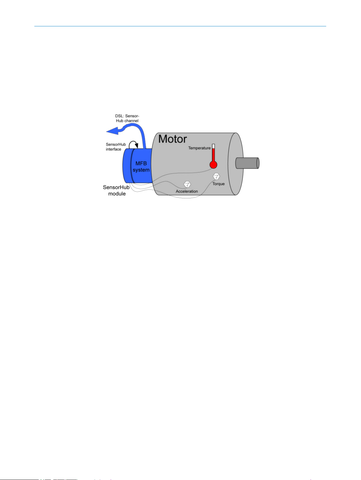
Data from additional external sensors can be transferred on the SensorHub Channel
that can be used in the frequency inverter system. External sensors must be connected
to the motor feedback system via the HIPERFACE DSL® SensorHub interface. Various
sensors or sensor networks are accessible via this interface and can be selected using
HIPERFACE DSL®.
8017595/ZTW6/2018-01-15 | SICK T EC H NI C AL IN F OR M AT I ON | HIPERFACE DSL
Subject to change without notice
®
13
Page 14
3 PROTOCOL OVERVIEW
The configuration of external sensors is carried out via the Parameters Channel, whilst
the data are transferred via the SensorHub Channel. The transfer of protocol packages
in the SensorHub Channel takes place synchronously with the DSL transfer and as an
extension of the frequency inverter cycle signal that is present at the DSL Master SYNC
input. Depending on the use of the SensorHub interface, external data can therefore be
sampled and transferred synchronously.
The protocol in the SensorHub Channel is not monitored by HIPERFACE DSL®. Apart
from the monitoring of the data transfer quality, there are no protocol mechanisms on
this channel.
Figure 4: HIPERFACE DSL® SensorHub interface
14
T EC H NI C AL IN F OR M AT I ON | HIPERFACE DSL
®
8017595/ZTW6/2018-01-15 | SICK
Subject to change without notice
Page 15

4 Hardware installation
The installation of HIPERFACE DSL® in a drive system requires an interface circuit with
specific components as well as the installation of a digital logic core for an FPGA com‐
ponent.
The interface circuit is described thoroughly in this chapter. The chapter also contains
recommendations for the selection of components.
The digital logic core (IP Core) is supplied by SICK for prescribed FPGA types.
In addition, the type of cable recommended for the connection between the frequency
inverter and the motor feedback system is described thoroughly in this chapter.
NOTE
It may also be possible to use other sorts of cable. These must be tested before use,
however.
As a physical layer, HIPERFACE DSL® uses a transfer in accordance with EIA-485
(RS-485).
4.1 Interface circuit
HARDWARE INSTALLATION 4
In most cases a transceiver for more than 20 MBaud is suitable. Nevertheless the tim‐
ing parameters of the transceiver have to fulfill the requirements of the following
table 3 under worst case conditions of the application.
Table 3: Interface circuit
Characteristic Value Units
Transfer rate >20 MBaud
Permitted common mode voltage -7 to +12 V
Receiver: Differential threshold voltage < 200 mV
Load resistance < 55 Ohm
Receiver running time delay < 60 ns
Sender running time delay < 60 ns
Sender power-up delay < 80 ns
Sender power-down delay < 80 ns
Sender rise time < 10 ns
Sender dropout time < 10 ns
Switch over time of 1 bit < 106.7 ns
Protection against short-circuit
Protection against bus conflict
HIPERFACE DSL® can be used in connection with two different interface circuit configu‐
rations. Each configuration requires a different sort of connection cable (see
chapter 4.3).
4.1.1 Separate encoder cable - four core cable
When using a separate encoder cable, the smallest interface circuit can be used. The
separate encoder cable allows a four core connection.
In connection with the associated table, figure 5 below gives the specification of the
interface circuit.
8017595/ZTW6/2018-01-15 | SICK T EC H NI C AL IN F OR M AT I ON | HIPERFACE DSL
Subject to change without notice
®
15
Page 16

DE
RE\
VCC
R
D
A
B
VSS
C1
C2
R1
R2
7..12 VDC
DATA+
DATA-
PWR+
PWR-
DSL
EN
DSL
IN
DSL
OUT
U2
DE
RE\
VCC
R
D
A
B
VSS
U2
C1
C2
R1
R2
TR1
C3
C4
7..12 VDC
L1
L2
DSL+
DSL-
DSL
EN
DSL
IN
DSL
OUT
4 HARDWARE INSTALLATION
Figure 5: Interface circuit with separate encoder cable
Recommended components for the interface circuit are set out in table 4.
Table 4: Components for the interface circuit with separate encoder cable
Component Part Manufacturer
C1 Ceramic capacitor 100 nF
C2 Ceramic capacitor 2.2 µF, 16 V
R1, R2 Resistors 56R
U2 RS485 transceiver SN65LBC176A
SN75LBC176A
Texas Instruments
Texas Instruments
NOTE
The use of four core cable is no longer recommended for the motor cable.
4.1.2 Integrated cable - two core cable
For a connection via a two core cable integrated in the motor cable, (see chapter 4.3),
the data cables must be provided with a transformer to raise the common mode rejec‐
tion ratio. To feed the supply voltage into the data cables choke coils are also required.
In connection with the associated table, figure 6 below gives the specification of the
interface circuit.
Figure 6: Interface circuit with two core cable (integrated in cable)
16
T EC H NI C AL IN F OR M AT I ON | HIPERFACE DSL
®
8017595/ZTW6/2018-01-15 | SICK
Subject to change without notice
Page 17

Recommended components for the interface circuit are set out in table 5.
Table 5: Components of the interface circuit with two core cable (integrated in cable)
Component Part Manufacturer
C1 Ceramic capacitor 100 nF
C2 Ceramic capacitor 2.2 µF, 16 V
C3, C4 Ceramic capacitor 470 nF, 50 V
L1, L2 Choke coils 744043101, 100 µH
R1, R2 Resistors 56R
U2 RS485 transceiver SN65LBC176A
TR1 Transformer PE-68386NL
4.1.3 Motor feedback voltage supply
Motor feedback systems with HIPERFACE DSL® have been developed for operation with
a supply voltage of 7 to 12 V. The voltage supply is measured at the encoder plug con‐
nector.
HARDWARE INSTALLATION 4
ELL6SH101M, 100 µH
SN75LBC176A
78602/1C
B78304B1030A003
78602/1C
Würth Elektronik
Panasonic
Texas Instruments
Texas Instruments
Pulse Engineering
Murata
Epcos
Epcos
table 6 below describes the specification for the power supply.
Table 6: Voltage supply
Parameter Value
Switch-on voltage ramp Max. 180 ms from 0 to 7 V
Inrush current Max. 3.5 A (0 to100 µs)
Operating current Max. 250 mA at 7 V
4.1.4 Interface circuit design recommendations
figure 5 and figure 6 show the two different interface circuits depending on the chosen
system configuration. The following recommendations help in attaining a system design
optimized for transmission robustness.
During PCB design a good RF isolation for the interface circuit shall be achieved
•
against the motor power circuit.
The two sides of the transformer TR1 have to be well separated from each other to
•
avoid crosstalk.
Inside the servo controller the DSL-signal lines shall be routed as short as possible
•
and with good symmetry in the differential part. To avoid or reduce signal distur‐
bances by EMC-noise it is recommended to place this circuit as close as possible
to the connection point of the DSL-lines.
During PCB layout design also assess and avoid potential EMC-noise coupling
•
from brake lines as well as the brake power supply circuit.
For the encoder power supply via L1/L2 a star connection to a very low impedance
•
point is important. Both inductances shall be well matched to each other to avoid
differential mode noise. Self-resonance frequency should be of at least 10 MHz. A
common mode filter between L1/L2 and the supply voltage can improve robust‐
ness.
The DSL-line impedance is matched balanced by 2 x 56 Ohm. C2 grounds remain‐
•
ing common mode noise after the transformer; RF parts shall be used or different
types paralleled to get low impedance on a broader frequency range. PCB design
Max. 1 A (100 µs to 400 µs)
8017595/ZTW6/2018-01-15 | SICK T EC H NI C AL IN F OR M AT I ON | HIPERFACE DSL
Subject to change without notice
®
17
Page 18

4 HARDWARE INSTALLATION
at this area needs to consider RF requirements for the actual components selec‐
tion and PCB layout.
DSL signal transmission is done with about 10 MHz frequency but square signal
•
harmonics can reach frequencies beyond (to 60 MHz) which should be considered
for layout design.
The used motor cable shall meet the impedance requirements of (110 +/-10)
•
Ohm to avoid signal reflections.
DSL line connection to the servo controller shall be separated from the motor
•
power connection point.
A good main shielding connection to a low inductance path shall allow draining
•
motor power residual current. For the DSL-line shielding a separate connection
point is recommended. For the connection unshielded DSL lines shall be avoided
or kept as short as possible (<20 mm).
4.2 FPGA IP Core
The frequency inverter system communicates with the DSL motor feedback system via
a special protocol logic circuit that is designated as the DSL Master. The circuit is sup‐
plied by SICK and must be installed in an FPGA component. It is supplied as an Intellec‐
tual Property Core (IP Core). The DSL Master IP Core is supplied in different forms,
depending on the FPGA vendor preferred by the user (compiled netlist or encrypted
VHDL). If there is sufficient space in the FPGA being used, the DSL Master can be
installed in the same component as the frequency inverter application.
CAUTION
There are two different IP Cores available, one for standard and one for safety applica‐
tions. This manual only describes the standard variant. Please choose according to the
desired system.
For interfacing the IP Core, several options are available. For details of those interface
blocks see chapter 9.1.
The following figure show the possible combinations of IP Core and interface block vari‐
ants.
18
T EC H NI C AL IN F OR M AT I ON | HIPERFACE DSL
®
8017595/ZTW6/2018-01-15 | SICK
Subject to change without notice
Page 19

Standard DSL Master
(dslm_n)
Parallel
interface
Parallel Bus Drive interface
SPI Pipeline
Test signals
Control signals
DSL
Standard DSL Master
(dslm_n)
Serial
interface
SPI Drive interface
SPI Pipeline
Test signals
Control signals
DSL
Standard DSL Master
(dslm_n)
User
interface
Miscellaneous Drive interface
SPI Pipeline
Test signals
Control signals
DSL
Serial
interface
SPI
A)
B)
C)
HARDWARE INSTALLATION 4
4.2.1 DSL Master inputs / outputs
8017595/ZTW6/2018-01-15 | SICK T EC H NI C AL IN F OR M AT I ON | HIPERFACE DSL
Subject to change without notice
Figure 7: Block diagrams of the "standard" DSL Master IP Core with interfaces
Table 7: Pin functions of the IP Core interface
Signal name Type Function
rst* Input Master reset (High active)
clk* Input Clock input
sync* Input Position sampling resolution
interrupt Output Configurable interrupt
link Output Connection indication
pos_ready Output Position data availability indication
sync_locked Output Position sampling resolution locked
bigend Input Byte sequence choice
fast_pos_rdy Output Fast position update indication
sample Output DSL bit sampling information
estimator_on Output Postion Estimator activated
safe_channel_err Output Transmission error in safe channel 1
safe_pos_err Output Safe position not valid
acceleration_err Output Fast channel / position error
acc_thr_err Output Fast channel / position threshold error
encoding_err Output DSL message encoding error
dev_thr_err Output Estimator deviation threshold reached
aux_signals Output (12) Auxiliary signals
dsl_in* Input DSL cable, input data
®
19
Page 20

rst
a b
Switch on
4 HARDWARE INSTALLATION
Signal name Type Function
dsl_out* Output DSL cable, output data
dsl_en* Output DSL cable transceiver, activation
spipipe_ss Input SensorHub SPI slave select
spipipe_clk Input Serial clock for SPI SensorHub
spipipe_miso Output SPI SensorHub, master output data/slave input
online_status_d Output (16) IP Core status information
hostd_a Input (7) Host interface address
hostd_di Input (8) Host interface data in
hostd_do Output (8) Host interface data out
hostd_r Input Host interface data read
hostd_w Input Host interface data write
hostd_f Input Host interface register freeze
* these signals must be assigned to physical pins of the FPGA.
4.2.2 SYNC signal
data
4.2.3 Reset signal
The HIPERFACE DSL® communication can be established in “SYNC mode” or “free run‐
ning mode”. In free running mode, the IP-Core will use the fastest possible transmis‐
sion timing and this input should be low (0). Please note that the IP-Core is not bound
to any timing of the frequency inverter in this mode.
In SYNC mode the frequency inverter clock must be supplied to this input/pin. Please
refer to table 8 for the signal specification. This signal triggers position sampling of the
DSL encoder. The polarity of the edge can be programmed using the SPOL bit in the
SYS_CTRL register.
As the frame cycle time must always be within a limited range, a divider for the SYNC
frequency has to be chosen accordingly. The divider value needs to be written to the
SYNC_CTRL register.
NOTE
In case of the SYNC frequency changing, the IP-Core will synchronize automatically. Dur‐
ing this synchronization the former sampling frequency is used. Please note that this
synchronization takes a few SYNC periods.
rst is the reset input (high active) of the DSL Master IP Core.
After start-up (switching on) of the frequency inverter, a reset procedure is mandatory to
return the DSL Master IP Core to its initialization condition.
The reset procedure is established by the parameters listed in table 8 and quoted in
figure 8.
20
Figure 8: Reset procedure
T EC H NI C AL IN F OR M AT I ON | HIPERFACE DSL
®
8017595/ZTW6/2018-01-15 | SICK
Subject to change without notice
Page 21

Table 8: Reset time sequence
Diagram reference Parameters in figure 8 Value (cf.figure 8)
a Reset delay Variable
b Duration of the reset signal >60 ns
Additional pin functions are described in detail in chapter 5.
4.3 Cable specification
HARDWARE INSTALLATION 4
The cable recommended for connecting the frequency inverter to the HIPERFACE DSL
®
motor feedback system is specified by the parameters set out in table 8. These techni‐
cal data apply to all configurations.
In the case of integrated cables (see chapter 4.1.2), the motor cables are not listed.
Table 9: Technical data for the HIPERFACE DSL® cable
Characteristic Minimum Typical Maximum Units
Length 100 m
Impedance at 10 MHz 100 110 120
DC loop resistance 0.1
W
W/m
Velocity ratio 0.66 c
Propagation delay 5 ns/m
Limit frequency 25 MHz
Maximum current per cable 0.25 A
Operating temperature -40 125 °C
More information relating cable construction and installation are available on the
Whitepaper “Cable and Connector for HIPERFACE DSL® Motor and Drive Applications”.
8017595/ZTW6/2018-01-15 | SICK T EC H NI C AL IN F OR M AT I ON | HIPERFACE DSL
Subject to change without notice
®
21
Page 22

Inverter
OK …
MFB
system
DSL
Response
Drive
Application
DSL
Master
DSL
Request
rst rst
clk clk
Drive interface Drive interface
SPI-PIPE SPI-PIPE
Control signals
Control signals
Test signals
Test signals
5 INTERFACES
5 Interfaces
The IP Core of the DSL Master includes interfaces to the motor feedback system (DSL
Slave) and to the frequency inverter application (see figure 9).
The motor feedback system communicates via a DSL connection with the DSL Master.
All data channels between the DSL Master and DSL Slave are routed via this connec‐
tion.
The user application is connected via one interface (choice of SPI or parallel bus) and
several control signals . In addition, the frequency inverter provides a clock signal (CLK)
and a reset signal (RST) to the DSL Master IP Core. By means of these signals, a
defined start-up performance is achieved.
According to the requirements of the particular application, an optional serial interface
(SPI-PIPE) can be employed to use the SensorHub Channel (see chapter 3.5).
The various interfaces correspond to the tasks described in table 10.
Figure 9: DSL system interfaces
Table 10: Interface functions
Interface Function
Drive interface Register-based access to all DSL Master and DSL Slave functions relevant
SPI PIPE Optional register-based access to SensorHub Channel data
Control signals DSL Master indication and control signals
Test signals Test signals for development or fault-finding for a DSL controller
CLK Clock signal for the IP Core circuit
RST Reset signal for the IP Core circuit
DSL Connection to the motor feedback system
5.1 Drive interface
The drive interface forms the central communications interface between the frequency
inverter application and the DSL Master IP Core. Absolute and fast position data can
be read via this interface. The functions of the motor feedback system are also accessi‐
22
T EC H NI C AL IN F OR M AT I ON | HIPERFACE DSL
ble via this interface.
The following signals are used for Drive interface:
Table 11: Drive interface signals
Pin name Type Function
online_status_d(0:15) Output IP Core status (see chapter 6.2)
®
for the core frequency inverter application
8017595/ZTW6/2018-01-15 | SICK
Subject to change without notice
Page 23

Pin name Type Function
hostd_a(0:6) Input Register address bus
hostd_di(0:7) Input Register input data bus
hostd_do(0:7) Output Register output data bus
hostd_r Input Read signal
hostd_w Input Write signal
hostd_f Input Freeze signal
Example installations of interface blocks for the Drive interface of the DSL Master are
supplied together with the IP Core. These examples include a serial SPI interface and a
parallel Texas Instruments EMIFA interface. For more information please see
chapter 9.1.
5.2 SPI PIPE Interface
The SPI PIPE is a read-only Serial Peripheral Interface (SPI). SPI PIPE is an optional com‐
munication channel between the frequency inverter application and the DSL Master IP
Core. Read processes on the SensorHub Channel can be carried out via this interface.
Alternatively, this data can also be read from the registers by standard transactions via
Drive interface.
INTERFACES
5
The type of access to the SensorHub Channel is selected by setting or deleting the
SPPE bits in the SYS_CTRL register (see chapter 6.3.1). If the SPPE bit is deleted, the
data and the status of the SensorHub channel are accessible via the DSL Master
PIPE_S (2Dh) and PIPE_D (2Eh) registers. If the SPPE bit is set, the SensorHub Channel
is read using the SPI PIPE "Read Pipeline" transaction.
SPI PIPE should be activated if, at a fast frequency inverter cycle, the bandwidth of
Drive interface is insufficient to access position and pipeline data, or if the pipeline
data is being processed by another frequency inverter application resource.
NOTE
It should be noted that in every case, the configuration of external sensor components
at the sHub® is carried out via the DSL Master Parameters Channel. The SPI PIPE pro‐
vides only one read access to the SensorHub Channel (see chapter 3.5).
The SensorHub Channel data is kept in a FIFO (First In First Out) buffer that can hold 8
bytes. In addition, for each data byte, status information is also stored in the FIFO buffer
(see chapter 6.3.22 and chapter 6.3.23).
NOTE
It should be noted that the FIFO buffer can only store 8 bytes of SensorHub Channel
data. If the buffer is not read quickly enough, old data will be overwritten. This is indi‐
cated by a flag in the FIFO buffer status information.
The SPI Master for the SPI PIPE is the frequency inverter application. The SPI functions
"Slave Selection" (Pin: spipipe_ss) and "clock" (Pin: spipipe_clk) are controlled by
the frequency inverter application. The SPI function "Data, Master input Slave output"
(Pin: spipipe_miso) is controlled by the DSL Master.
SPI PIPE has the following SPI characteristics:
PHA = 1 (Sampling for clock trailing edge, data changes for clock leading edge)
•
POL = 0 (Basic clock value)
•
The data with the highest value bit (MSB) is given first.
8017595/ZTW6/2018-01-15 | SICK T EC H NI C AL IN F OR M AT I ON | HIPERFACE DSL
Subject to change without notice
®
23
Page 24

spipipe_clk
spipipe_miso
POL=0
PHA=1
1 2 3 4 5 6 7 8
a
b c
n-1 n
d
e
f
spipipe_ss
spipipe_clk
spipipe_miso
PIPE STATUS PIPE DATA
spipipe_ss
5 INTERFACES
When accessing the SensorHub Channel via the SPI PIPE, the first four bits of the sta‐
tus buffer (0101) show a different value for each transaction, in order to check the cor‐
rect function of the interface.
5.2.1 SPI-PIPE timing
The time sequence for SPI PIPE is shown in the time sequence diagram (figure 10 )
below and in table 12.
Figure 10: SPI-PIPE interface time control
Table 12: SPI-PIPE time control
Diagram
reference
Description Mini‐
mum
Maxi‐
mum
Units
A Assertion of spipipe_ss before spipipe_clk 30 ns
B Time for spipipe_clk high 30 ns
C Time for spipipe_clk low 30 ns
D spipipe_ss pulse width 30 ns
E Delay spipipe_miso after spipipe_ss high 25 70 ns
F Delay spipipe_miso after spipipe_clk high 25 70 ns
5.2.2 Read pipeline
The SPI PIPE transaction "Read Pipeline" is used for access to the FIFO buffer values
that contain the data and status of the SensorHub Channel.
Table 13: "Read Pipeline" transaction
Symbol Meaning
PIPE STATUS SensorHub Channel status (see chapter 6.3.21)
PIPE DATA SensorHub Channel data (see chapter 6.3.22)
Figure 11: "Read Pipeline" transaction
5.3 Control signals
Various control signals are available between the DSL Master and the frequency
inverter application to configure the performance of the IP Core or to carry out fast
monitoring of the IP Core status.
5.3.1 SYNC signal
sync is a DSL Master digital input.
24
T EC H NI C AL IN F OR M AT I ON | HIPERFACE DSL
®
8017595/ZTW6/2018-01-15 | SICK
Subject to change without notice
Page 25

One edge on this pin triggers a position sampling. The polarity of the edge can be pro‐
grammed using the SPOL bit in the SYS_CTRL (00h) register. The protocol requires a
constant frequency of the signal at this pin, with deviations permitted within a set toler‐
ance band. Continuously, the protocol synchronizes the protocol frame with the signal
frequency at sync.
NOTE
If the sync signal frequency is outside the tolerance range, re-synchronization of the
protocol is triggered. During the time that the re-synchronization is taking place, sam‐
pling is carried out with the former sync frequency until the re-synchronization is com‐
plete. For more details on the sync signal also see chapter 7.3.3.
5.3.2 INTERRUPT signal
interrupt is a DSL Master digital output.
interrupt is set to "1" if an interrupt condition has been fulfilled in the DSL-Master.
The interrupt conditions are set using the registers MASK_H, MASK_L and MASK_SUM
(see chapter 6.3.5 and chapter 6.3.6).
NOTE
During each write process in one of the registers EVENT_H or EVENT_L, the interrupt
output is masked until the current SPI transaction has ended.
INTERFACES 5
5.3.3 LINK signal
link is a DSL Master digital output.
link is effected by the content of the LINK bit in the MASTER_QM register (see
chapter 6.3.3) and therefore indicates whether the DSL Master has produced a com‐
munications link to a connected HIPERFACE DSL® motor feedback system.
link is intended to be a control signal for an LED display, but can also be used to con‐
trol the start-up performance (see chapter 7.1) or for global error handling.
link is reset if communication faults are detected.
5.3.4 FAST_POS_RDY signal
fast_pos_rdy is a DSL Master digital output.
fast_pos_rdy signals that a new fast position value is available and permits an
event-based reading of the position for incorporating latency reduction.
fast_pos_rdy is always available, even if the position value is invalid or no connec‐
tion to the encoder has been established.
Dependent upon the configuration in the register system control (see chapter 6.3.1),
fast_pos_rdy displays either only the availability of positions based on user require‐
ments (edge at sync input) or all transmitted positions.
5.3.5 SYNC_LOCKED signal
sync_locked is a DSL Master digital output.
sync_locked indicates whether the sync signal was correctly passed to the encoder,
or whether the IP Core is still in a synchronization phase. sync_locked drops to “0”
when the SYNC edge supplied by the application has been transported with more than
2 clock cycles of distortion.
8017595/ZTW6/2018-01-15 | SICK T EC H NI C AL IN F OR M AT I ON | HIPERFACE DSL
Subject to change without notice
®
25
Page 26

5 INTERFACES
5.3.6 BIGEND signal
5.4 Test signals
5.4.1 SAMPLE signal
bigend is a DSL Master digital input.
The byte sequence of the address allocation for registers can be influenced via bigend
(see chapter 9.5). The byte sequence is based on 32 bit-wide data words. The selection
influences the allocation independently of the interface block used.
Table 16 below lists the selection options for bigend.
Table 14: bigend selection
Value Address allocation byte sequence
0 Little endian
1 Big endian
To support development or fault-finding for controllers that have a DSL interface inte‐
grated, the DSL Master supplies some test signals.
sample is a DSL Master digital output.
The sample signal is set at the sampling time point of each bit that is transmitted from
the DSL motor feedback system. It consists of 50 pulses from Channel 1 followed by a
bit pause and 10 pulses from Channel 2 of the motor feedback system.
Figure 12: Sample signal
The sample signal can be used for eye diagrams to measure time and voltage margins
during signal transmission.
When making the evaluation, signal delays in the DSL Master must be taken into
account. The rising edge of the sample signal is offset by 40 ns from the line driver
signal. The time delay of the line driver must also be taken into account. Typically this is
13 ns.
5.4.2 ESTIMATOR_ON signal
estimator_on is a DSL Master digital output.
26
The estimator_on signal is set if some event leads to the transmitted fast position
(see chapter 6.3.12) being invalid and the position estimator supplying the values.
Such events are:
The DSL motor feedback system reporting a position error
•
A coding error in transmission of the fast position
•
A check-sum error in transmission of the fast position
•
Realignment from safe to fast - fast position is forced to the safe position value
•
The protocol is re-synchronizing following a break in the link
•
T EC H NI C AL IN F OR M AT I ON | HIPERFACE DSL
®
8017595/ZTW6/2018-01-15 | SICK
Subject to change without notice
Page 27

The estimator_on signal can be used to carry out a statistical analysis of the inci‐
dence of errors in the DSL system. For more information, please refer to chapter 7.3.1.
It should be noted that the POS flag and estimator_on signal information is redun‐
dant.
5.4.3 DEV_THR_ERR signal
dev_thr_err is a DSL Master digital output.
If the fast position from the process data channel cannot be calculated (either due to
transmission or due to sensor errors), estimation is made by the DSL Master based on
the last two available position values of the Safe Channel. The worst case deviation
from the actual mechanical position is also provided, referring to a user- defined para‐
meter for the maximum possible acceleration in the application (fast position accelera‐
tion boundary, see chapter 6.3.25).
A threshold can be set up for a worst case deviation to raise the dev_thr_err out-
put. The threshold is a user defined parameter for the maximum tolerable deviation in
the application (fast position estimator deviation, see chapter 6.3.26).
dev_thr_err indicates whether the maximum tolerable deviation is violated (‘1’) or
kept (‘0’).
INTERFACES 5
5.4.4 SAFE_CHANNEL_ERR signal
safe_channel_err is a DSL Master digital output.
The safe_channel_err signal is set if some event leads to the safe position or sta‐
tus (see chapter 6.3.15) being invalid. Such events are:
A coding error in transmission of the safe position
•
A check-sum error in transmission of the safe position
•
The safe_channel_err signal can be used to carry out a statistical analysis of the
incidence of errors in the DSL system.
5.4.5 SAFE_POS_ERR signal
safe_pos_err is a DSL Master digital output.
safe_pos_err is a DSL Master digital output. The safe_pos_err signal is set if the
safe position of Safe Channel 1 is not updated or it has never been written since the
startup. Another possible cause can be the DSL motor feedback system reporting a
position error.
5.4.6 ACCELERATION_ERR signal
acceleration_err is a DSL Master digital output.
The acceleration_err signal is set if an encoding error was detected after transmis‐
sion of a fast position value, or if the encoder has transmitted an invalid acceleration
cause of internal errors.
If the acceleration_err signal is set the error counter acc_err_cnt will be incre‐
mented with each transmission (see chapter 6.3.24). As soon as the accelera-
tion_err signal is reset the error counter acc_err_cnt will be set to “0” again.
5.4.7 ACC_THR_ERR signal
acc_thr_err is a DSL Master digital output.
The acc_thr_err signal is set if the threshold programmed in register
acc_err_cnt is exceeded.
8017595/ZTW6/2018-01-15 | SICK T EC H NI C AL IN F OR M AT I ON | HIPERFACE DSL
Subject to change without notice
®
27
Page 28

5 INTERFACES
The acc_thr_err signal can be used to implement a fault-tolerant evaluation in the
drive. For this the maximum position deviation should be calculated from the number of
transmission errors.
5.4.8 ENCODING_ERR signal
encoding_err is a DSL Master digital output.
The encoding_err signal is set if the underlying 8B/10B encoding of a DSL frame
transmission is disturbed.
The encoding_err signal can be used to make a statistical analysis of the bit error
rate of a DSL system.
28
T EC H NI C AL IN F OR M AT I ON | HIPERFACE DSL
®
8017595/ZTW6/2018-01-15 | SICK
Subject to change without notice
Page 29

6 Register map
DSL Master Primary
functions
Registers
for all
main
functions
00h
01h
|
|
2Dh
2Eh
|
3Eh
3Fh
Drive interfacexx
SPI-PIPEx
DSL
Slave
Remote
Registers
40h
41h
|
|
|
7Eh
7Fh
(optional)
The DSL Master is accessible via register in three different register blocks. Each register
block has its own address area (see table 15).
Table 15: Register blocks address area
Register block Address area Functions
Drive 00h to 3Fh
Safe 1 00h to 7Fh Safe Channel 1, position/status
Safe 2 00h to 3Fh Safe Channel 2, position/status
All IP Core registers and functions can be accessed via drive interface. As an option, the
SensorHub Channel data is accessible via the SPI PIPE interface.
In addition, the DSL Slave interface registers are mirrored as decentralized registers.
The address area 40h to 7Fh is intended for this. The addressing of these registers is
identical to the addressing of the registers in the DSL Master. The answer to the trans‐
action is, however, delayed and must be read individually (see under "Short message",
in chapter 7.5.1).
60h to 6Fh
REGISTER MAP 6
Process data Channel, position/status
Parameters Channel (long messages)
SensorHub Channel
Parameters Channel (short messages)
6.1
8017595/ZTW6/2018-01-15 | SICK T EC H NI C AL IN F OR M AT I ON | HIPERFACE DSL
Subject to change without notice
figure 13 below shows via which interface a connection to which register block is estab‐
lished.
Figure 13: Register block overview
Explanation of the registers
In the following description of the registers, symbols are used to describe the standard
value of a bit following a reset. Additional symbols are used to describe the functions
provided to the frequency inverter application for this bit.
®
29
Page 30

REGISTER MAP
6
The bit is described according to the following example: "Function" "Reset value", e.g.
"R/W-0"
Table 16: Function symbols for bits
Function symbol Meaning
R Bit can be read.
W Bit can be set and deleted.
C Bit can only be deleted.
X Bit is not installed and will always be read as "0".
Table 17: Symbols for bit reset values
Reset value Meaning
0 The bit is deleted after a reset.
1 The bit is set after a reset.
x After a reset, the bit has no defined value.
- In the register diagram:
The bit is not installed and will always be read as "0".
NOTE
It should be noted that read access to a bit that can only be written ("W") always returns
the value "0". If a register address that is not used is read, the result will be “0” as well.
6.2 Online Status D
The Online Status D is a non-storing copy of registers EVENT_H and EVENT_L. The sta‐
tic information in these registers must be deleted by the user after the read process, by
writing the value "0" to the corresponding bit in the register, whilst the Online Status D
only shows the current status without storing previous indications. The signal name of
the Online Status is online_status_d (with d indicating drive).
online_status_d is given in two bytes. If an SPI block is used for interfacing the IP
Core, online_status_d is transmitted in each transaction in the first two bytes via
the spi_miso output. When a parallel bus interface is used for drive interface,
online_status_d has 16 dedicated output signals available.
NOTE
It should be noted that when the parallel bus interface is used the 16 signals of the
Online Status D are not frozen during a read access. If required, the user can insert a
Latch (e.g. using the hostd_fcode.inlinesignal).
Table 18: Online Status D, High Byte
Bit 7
INT: Status of the Interrupt output
R-0 R-0 R-1 R-1 R-1 R-1 R-1 R-1
INT SUM SCE FIX1 POS VPOS DTE PRST
Bit 7 Bit 0
30
This bit represents an exception to the Online Status D, as this bit does not relate to an
event indication. INT provides the value of the physical INT output so that request man‐
agement (polling) can be established. The importance of this flag depends on the Inter‐
rupt sources monitored.
1 = interrupt output on "High" level
0 = interrupt output on "Low" level
T EC H NI C AL IN F OR M AT I ON | HIPERFACE DSL
®
8017595/ZTW6/2018-01-15 | SICK
Subject to change without notice
Page 31

Bit 6 SUM: Summary byte
1 = The last valid value from SUMMARY was not zero. The importance of this flag
depends on the particular error source that leads to a set SUMMARY (see
chapter 6.3.14).
0 = The last valid value from SUMMARY was zero.
REGISTER MAP
6
Bit 5
SCE: CRC error on the Safe Channel
1 = The last Safe Channel CRC received was wrong. It is expected that the last safe
position transmitted (see chapter 6.3.16) is invalid.
0 = The last Safe Channel CRC received was correct.
Bit 4 FIX1: This bit always gives a "1". For SPI interfaces, this is used for checking the
spi_miso pin for stuck-at- '0' faults.
Bit 3 POS: Estimator turned on (functionality based on estimator_on, see chapter 5.4.2)
1 = A source of an error in the fast position was identified or an alignment procedure is
currently being carried out. It is probable that the last fast position is invalid. Be aware
that the fast position read through drive interface is provided by the estimator.
0 = No fast position error.
Bit 2
VPOS: Safe position invalid
1 = An error in the safe position was identified. It is expected that the safe position
transmitted from the encoder is invalid.
0 = The last safe position received was correct.
Bit 1 DTE: Deviation Threshold Error (see chapter 5.4.3)
1 = Current value of deviation greater than the specified maximum.
0 = Current value of deviation smaller than the specified maximum.
Bit 0 PRST: Protocol reset
1 = IP-Core has restarted the protocol.
0 = IP-Core running.
Table 19: Online Status D, Low Byte
X-0 X-0 R-0 R-0 R-0 R-1 R-0 R-0
POSTX MIN ANS FIX0 QMLW FREL FRES
Bit 7 Bit 0
Bit 7-6 POSTX1:POSTX0: Position transmission status
00: Position request is transmitted to the DSL encoder.
01: Safe Channel was correctly transmitted.
10: Fast position present (see chapter 6.3.11).
11: Safe Channel 2 was correctly transmitted.
Recommended to trigger on rising edge of a POSTX bit change (is set). A new state is
indicated by a set bit. It is cleared/maintained until a new frame/event arrives.
Bit 5
MIN: Acknowledgment of message initialization
1 = The DSL encoder sends a figure by which the initialization of the Parameter Chan‐
nel is acknowledged.
0 = Parameter Channel not functioning.
Bit 4
ANS: Incorrect answer detected.
8017595/ZTW6/2018-01-15 | SICK T EC H NI C AL IN F OR M AT I ON | HIPERFACE DSL
Subject to change without notice
®
31
Page 32

6 REGISTER MAP
1 = The last answer to a long message was damaged.
0 = No error detected in the last answer to a long message.
Bit 3 FIX0: This bit always gives a "0". For SPI interfaces, this is used for checking the
spi_miso pin for stuck-at-'1' faults.
Bit 2 QMLW: Quality monitoring at Low level (see chapter 6.3.3)
1 = Current value of quality monitoring less than 14.
0 = Current value of quality monitoring greater than or equal to 14.
Bit 1 FREL: Channel status for “long message”.
1 = The channel for the “long message” is free.
0 = The channel for the “long message” is in use.
Bit 0 FRES: Channel status for the "short message". 1 = The channel for the "short message"
is free.
0 = The channel for the "short message" is in use.
6.3 DSL Master function register
The protocol logic controls the performance of the DSL Master via the registers in the
DSL Master IP Core on drive interface. These registers are also used for accessing the
position values.
The table below contains a list of all the function registers available in the IP Core.
NOTE
The addresses given below are referencing a big-endian addressing. For a table stating
the register addresses depending on the endianness, see chapter 9.5.
Table 20: Description of the registers in DSL Master, drive interface
Addr Designation Bit 7 Bit 6 Bit 5 Bit 4 Bit 3 Bit 2 Bit 1 Bit 0 Value at reset
00h SYS_CTRL PRST MRST FRST LOOP PRDY SPPE SPOL OEN 0000 0000
01h SYNC_CTRL ES 0000 0001
03h MASTER_QM LINK - - -
04h EVENT_H INT SUM SCE - POS VPOS DTE PRST 000- 0000
05h EVENT_L - - MIN ANS - QMLW FREL FRES --00 -000
06h MASK_H - MSUM MSCE - MPOS MVPOS MDTE MPRST -00- 0000
07h MASK_L - - MMIN MANS - MQMLW MFREL MFRES --00 -000
08h MASK_SUM MSUM7:0 0000 0000
09h EDGES Bit sampling pattern 0000 0000
0Ah DELAY RSSI Cable delay 0000 0000
0Bh VERSION Coding
0Ch RELEASE Release date FIFO 0000 0000
0Dh ENC_ID2 - SCI ENC_ID19:16 -000 0000
0Eh ENC_ID1 ENC_ID15:8 0000 0000
0Fh ENC_ID0 ENC_ID7:0 0000 0000
10h POS4 Fast position, byte 4 0000 0000
11h POS3 Fast position, byte 3 0000 0000
12h POS2 Fast position, byte 2 0000 0000
IP Core version number
Quality monitoring
0--- 0000
0101 0111
32
T EC H NI C AL IN F OR M AT I ON | HIPERFACE DSL
®
8017595/ZTW6/2018-01-15 | SICK
Subject to change without notice
Page 33

REGISTER MAP 6
Addr Designation Bit 7 Bit 6 Bit 5 Bit 4 Bit 3 Bit 2 Bit 1 Bit 0 Value at reset
13h POS1 Fast position, byte 1 0000 0000
14h POS0 Fast position, byte 0 0000 0000
15h VEL2
Speed, byte 2
16h VEL1 Speed, byte 1 0000 0000
17h VEL0 Speed, byte 0 0000 0000
18h SUMMARY SUM7:0 0000 0000
19h VPOS4
Safe position, byte 4
1Ah VPOS3 Safe position, byte 3 0000 0000
1Bh VPOS2 Safe position, byte 2 0000 0000
1Ch VPOS1 Safe position, byte 1 0000 0000
1Dh VPOS0 Safe position, byte 0 0000 0000
1Eh VPOSCRC_H CRC of the safe position, byte1 0000 0000
1Fh VPOSCRC_L CRC of the safe position, byte0 0000 0000
20h PC_BUFFER0
Parameters Channel, byte0
21h PC_BUFFER1 Parameters Channel, byte1 0000 0000
22h PC_BUFFER2 Parameters Channel, byte2 0000 0000
23h PC_BUFFER3 Parameters Channel, byte3 0000 0000
24h PC_BUFFER4 Parameters Channel, byte4 0000 0000
25h PC_BUFFER5 Parameters Channel, byte5 0000 0000
26h PC_BUFFER6 Parameters Channel, byte6 0000 0000
27h PC_BUFFER7 Parameters Channel, byte7 0000 0000
28h PC_ADD_H LID LRW LOFF LIND LLEN LADD9:8 1000 0000
29h PC_ADD_L LADD7:0 0000 0000
2Ah PC_OFF_H LID LOFFADD14:8 1000 0000
2Bh PC_OFF_L LOFFADD7:0 0000 0000
2Ch PC_CTRL - - - - - - - LSTA ---- ---0
2Dh PIPE_S - - - - POVR PEMP PERR PSCI ---- 0000
2Eh PIPE_D SensorHub FIFO, output 0000 0000
2Fh PC_DATA
"Short message" data
38h ACC_EE_CNT - - - Acc. errorthreshold/counter ---0 0000
39h MAXACC Acc. Res. Acc. Mantissa 1111 1111
3Ah MAXDEV_H Max. position deviation, byte1 0000 0000
3Bh MAXDEV_L Max. position deviation, byte0 0000 0000
3Fh DUMMY No data ---- ----
0000 0000
0000 0000
0000 0000
0000 0000
NOTE
It should be noted, that some registers are shared (e.g. 09h EDGES) and others are just
used for accessing the same data (SYS_CTRL and SAFE_CTRL, for instance). In most
cases though, both interfaces use registers that are exclusively available to them.
6.3.1 System control
The system control register SYS_CTRL contains the main control bits of the DSL Master.
8017595/ZTW6/2018-01-15 | SICK T EC H NI C AL IN F OR M AT I ON | HIPERFACE DSL
Subject to change without notice
®
33
Page 34

6 REGISTER MAP
Register 00h: System control
Bit 7 PRST: Protocol reset
Bit 6 MRST: Messages reset
NOTE
It should be noted that apart from a reset of the Master, all system control bits can only
be set and deleted by the user.
R/W-0 R/W-0 R/W-0 R/W-0 R/W-0 R/W-0 R/W-0 R/W-0
PRST MRST FRST LOOP PRDY SPPE SPOL OEN
Bit 7 Bit 0
1 = A forced reset of the protocol status will be initiated. If the bit is deleted, a restart of
the connection is triggered.
0 = Normal protocol action
1 = The Parameters Channel is reset. Current short and long messages are discarded.
0 = Normal Parameters Channel action
Bit 5
FRST: Pipeline FIFO, reset
1 = The FIFO is reset. Data is not stored and cannot be read.
0 = Normal FIFO access
Bit 4
LOOP: Test drive interface
Value for the read back test for drive interface. This value has no other purpose.
Bit 3 PRDY: POS_READY mode.
1 = pos_ready shows time of receipt of all position transmissions.
0 = pos_ready shows only the time of receipt of position transmissions following a
control clock (sync input).
Bit 2 SPPE: SPI-PIPE activation
1 = SPI-PIPE activated. Access to pipeline status and data via SPI-PIPE. The registers
PIPE_S and PIPE_D are read as "0".
0 = SPI-PIPE deactivated. Access to pipeline status and data via the registers PIPE_S
and PIPE_D.
Bit 1 SPOL: Polarity of the synchronization pulse
1 = The sync trailing edge is used.
0 = The sync leading edge is used.
Bit 0 OEN: Activation of the output
1 = The DSL cables are activated for output to the DSL Slave.
0 = The impedance of the DSL cable is high.
6.3.2 Synchronization control
The SYNC_CTRL register for control of the synchronization contains the bit with which
the synchronization source for position sampling is controlled.
Register 01h: Synchronization control
W-0 W-0 W-0 W-0 W-0 W-0 W-0 W-1
34
T EC H NI C AL IN F OR M AT I ON | HIPERFACE DSL
ES
®
8017595/ZTW6/2018-01-15 | SICK
Subject to change without notice
Page 35

Bit 7-0 ES: External synchronization
00000000 = Position sampling during free running at the shortest cycle time.
All other values = Position sampling with the sync signal synchronized. The value from
ES determines the number of position samplings carried out in one sync cycle. The
user must match the number of samplings per cycle to the shortest frame length (see
chapter 7.3.3).
6.3.3 Quality monitoring
The MASTER_QM quality monitoring register contains the quality monitoring value for
the data connection.
As soon as the DSL Master detects events that indicate an improvement or degradation of the quality of the data connection, these events are indicated as values higher
or lower than the quality monitoring value (see table 21).
Table 21: Quality monitoring events
Protocol event Value change in quality moni‐
Wrong synchronization in Safe Channel (last byte) -4
Wrong synchronization in Safe Channel (1
RSSI <2 -4
Wrong encoding in parameter or SensorHub channels -1
Wrong encoding in process data channel -2
Unknown special characters in the protocol package -2
Any identified error in Safe Channel 1 -6
Any identified error in Safe Channel 2 -8
Correct synchronization in Safe Channel +1
Correct CRC value in Safe Channel +1
REGISTER MAP 6
Bit 7 Bit 0
toring
st
th
… 7
bytes) -6
Quality monitoring is initiated with the value "8".
The maximum quality monitoring value is "15". This is the standard value during opera‐
tion.
NOTE
Particular attention must be paid to the quality monitoring value during the develop‐
ment of a DSL drive controller. If a value lower than "15" is indicated, the cause may be
a problem with the connection circuit, particularly if the value is continuously displayed.
If the quality monitoring value falls below "14", QMLW information is indicated in Online
Status and in the EVENT_L register.
If the quality monitoring value falls to "0", a forced reset of the protocol is carried out.
This is indicated by the PRST error bit in Online Status and in the EVENT_H register.
The MASTER_QM register is write protected.
Register 03h:
Quality monitoring register
R-0 X-0 X-0 X-0 R-0 R-0 R-0 R-0
LINK QM
Bit 7 Bit 0
8017595/ZTW6/2018-01-15 | SICK T EC H NI C AL IN F OR M AT I ON | HIPERFACE DSL
Subject to change without notice
®
35
Page 36

REGISTER MAP
6
Bit 7 LINK: DSL protocol connection status
1 = Protocol connection between DSL Master and Slave was established.
0 = No connection present or connection error due to a communications error.
It should be noted that LINK is also represented at the link interface output (see
chapter 5.3).
Bit 6-4 Not implemented: Read as "0".
Bit 3-0
6.3.4 Events
QM3:QM0: Quality monitoring bits
0000 to 1111: Quality monitoring value. Higher values indicate a better connection. If
the quality monitoring reaches the value "0000", a forced reset of the protocol is car‐
ried out.
The EVENT_H/EVENT_L registers contain the messaging bits for all warning and error
modes of the DSL system.
All messaging bits are set by the DSL Master if a corresponding status is determined.
The following bit description lists the effects of warning and error conditions as well as
the reactions to errors that must be installed in the frequency inverter application.
An event bit that has been set is not reset by the DSL Master. The frequency inverter
application must delete bits that have been set.
Both edge and level-sensitive flags are present in the EVENT registers. Edge- sensitive
bits are set when the corresponding status arises. They are only set again if the corre‐
sponding status disappears and then arises once more. This is the standard action. The
level-sensitive bits set a bit as long as the corresponding status exists.
NOTE
It should be noted that all event register bits are also transferred to Online Status D
(see chapter 6.2 and chapter 7.6.2). The event bits are not static there and contain the
actual status of each individual event.
36
Register 04h:
High Byte events
R-0 R/C-0 X-0 X-0 R/C-0 X-0 R/C-0 R/C-0
INT SUM POS DTE PRST
Bit 7 Bit 0
Bit 7 INT: Interrupt status
This bit reflects the status of the interrupt signal (see chapter 5.3.2).
Bit 6
SUM: Remote event monitoring
1 = The DSL Slave has signaled an event and the summary mask is set accordingly (see
registers MASK_SUM and SUMMARY).
0 = All DSL Slave events are deleted.
When the SUM bit is set, an error or a warning has been transmitted from the DSL
Slave. The frequency inverter application must check the SUMMARY register (see
chapter 6.3.14) to obtain a detailed description. This bit is level sensitive.
Bit 5 SCE: Error on the Safe Channel
1 = Data consistency error on the Safe Channel.
0 = Safe Channel data was correctly transmitted.
T EC H NI C AL IN F OR M AT I ON | HIPERFACE DSL
®
8017595/ZTW6/2018-01-15 | SICK
Subject to change without notice
Page 37

This error usually indicates a transmission error on the DSL connection. If this error
occurs frequently, the wiring of the DSL connection should be checked. If this error
occurs continuously, there is probably an error in the motor feedback system.
This error affects quality monitoring and produces the QMLW warning or a protocol
reset.
: Read as "0".
CAUTION
When this error occurs, the last valid value of the safe position is retained (see
chapter 6.3.15). Only if a fresh value has been transmitted will the safe position be
updated and correspond to the actual position of the motor feedback system. The fast
position is not affected by this.
Bit 4 Not implemented: Read as "0".
REGISTER MAP
6
Bit 3
Bit 2
POS: Estimator turned on (functionality based on estimator_on, see chapter 5.4.2)
1 = Fast position data consistency error. The fast position read through drive interface
is supplied by the estimator.
0 = The data for the fast position was correctly transmitted.
This error usually indicates a transmission error on the DSL connection. If this error
occurs frequently, the wiring of the DSL connection should be checked. If this error
occurs continuously, there is probably an error in the motor feedback system.
CAUTION
When this error occurs, the fast position is updated by the estimator (see
chapter 7.3.1).
VPOS: Safe position error 1 = Sensor error.
0 = The safe position is correct.
This error usually indicates an encoder sensor error. If this error occurs continuously,
there is probably an error in the motor feedback system.
CAUTION
When this error occurs, the error value FD FD FD FD FDh is displayed instead of the
safe and fast position.
Bit 1
DTE: Estimator Deviation Threshold Error (see chapter 5.4.3)
1 = Current value of deviation greater than the specified maximum.
0 = Current value of deviation smaller than the specified maximum.
CAUTION
This error message is relevant when the estimator deviation threshold is used. See
chapter 7.3.1 for details of this function.
Bit 0
PRST: Protocol reset warning
1 = The forced protocol reset was triggered.
0 = Normal protocol action
8017595/ZTW6/2018-01-15 | SICK T EC H NI C AL IN F OR M AT I ON | HIPERFACE DSL
Subject to change without notice
®
37
Page 38

REGISTER MAP
6
This error message indicates that the protocol connection to the DSL Slave has been reinitialized. This error message can be caused by a frequency inverter application
request (PRST bit in SYS_CTRL), generated by the DSL Master itself, or activated via the
rst input.
The DSL Master causes a protocol reset if too many transmission errors indicate a con‐
nection problem (see chapter 6.3.3). A protocol reset causes a re-synchronization with
the DSL Slave that can improve the connection quality.
Register 05h:
Low Byte events
X-0 X-0 R/C-0 R/C-0 R/C-0 R/C-0 R/C-0 X-0
Bit 7 Bit 0
Bit 7-6 Not implemented: Read as "0".
Bit 5 MIN: Message initialization
1 = An acknowledgment was received from the Slave for the initialization of a message.
0 = No acknowledgment for the initialization received.
When this warning is displayed, the Parameters Channel is still in the initialization sta‐
tus and no "short message" or "long message" can be triggered.
This bit is level sensitive.
Bit 4 ANS: Erroneous answer to "long message"
1 = An error occurred during the answer to a long message. The effectiveness of the
previous transaction is not known.
0 = The last answers to "long messages" were error free.
This error indicates that the transmission of an answer from the DSL Slave to the last
"long message" failed. The frequency inverter application must send the "long mes‐
sage" again.
MIN ANS QMLW FREL
Bit 3 Not implemented: Read as "0".
Bit 2 QMLW: Quality monitoring low value warning
1 = Quality monitoring value (see register 03h) below "14"
0 = Quality monitoring value greater than or equal to "14"
This warning indicates that a transmission error occurred at bit level for one of the CRC
values. If this error occurs frequently, the wiring of the DSL connection should be
checked (also see chapter 6.3.3).
Bit 1 FREL: Channel free for "long message"
1 = A "long message" can be sent on the Parameters Channel.
0 = No "long message" can be sent.
If the bit is set, the frequency inverter application can trigger a "long message". Pro‐
vided no answer has been received from the DSL Slave, this bit remains deleted. As the
processing duration of a "long message" in the motor feedback system is not specified,
a user time limit condition should be installed via the frequency inverter application.
When a time limit is exceeded, the MRST bit in the SYS_CTRL register is set, which
causes the Parameters Channel to be reset.
Bit 0
FRES: Channel free for "short message"
1 = A "short message" can be sent on the Parameters Channel.
0 = No "short message" can be sent.
38
T EC H NI C AL IN F OR M AT I ON | HIPERFACE DSL
®
8017595/ZTW6/2018-01-15 | SICK
Subject to change without notice
Page 39

6.3.5 Event mask
OR
Events (DSL Master)
Reg
04h
Reg
05h
--
PRST
DTE
POS
SCE
--
VPOS
SUM
--
FRES
FREL
--
MIN
ANS
QMLW
--
Status (DSL Slave)
Reg
18h
SUM7
SUM0
SUM1
SUM3
SUM5
SUM4
SUM2
SUM6
INT output
OR
Event Mask
Reg
06h
Reg
07h
--
MPRST
MDTE
MPOS
MSCE
--
MVPOS
MSUM
--
MFRES
MFREL
--
MMIN
MANS
MQMLW
--
Status Mask
Reg
08h
MSUM7
MSUM0
MSUM1
MSUM3
MSUM5
MSUM4
MSUM2
MSUM6
REGISTER MAP
If the bit is set, the frequency inverter application can trigger a "short message". Pro‐
vided no answer has been received from the DSL Slave, this bit remains deleted. As the
processing duration of a "long message" in the motor feedback system is not specified,
a time limit condition is installed in the DSL Master. If the time limit is exceeded,
attempts are made again automatically (see under RET bit).
In the event mask registers MASK_H/MASK_L, the events are set with which the inter-
rupt signal is set.
Several events can be masked to trigger an interrupt. In addition, events from the DSL
Slave summary can be combined with these events (see chapter 6.3.6). This is
explained in figure 14 .
6
8017595/ZTW6/2018-01-15 | SICK T EC H NI C AL IN F OR M AT I ON | HIPERFACE DSL
Subject to change without notice
Register 06h:
Figure 14: Interrupt masking
NOTE
It should be noted that the SUM bit is an OR connection of all bits of the status bit is an
OR connection of all bits of the status summary (SUMMARY register).
High Byte event mask
X-0 W-0 X-0 X-0 W-0 X-0 W-0 W-0
MSUM MPOS MDTE MPRST
Bit 7 Not implemented: Read as "0".
Bit 6
Bit 7 Bit 0
MSUM: Mask for remote event monitoring
1 = DSL Slave events that are masked in the SUMMARY register set the interrupt sig‐
nal.
0 = DSL Slave events that are masked in the SUMMARY register do not set the inter-
rupt signal.
®
39
Page 40

REGISTER MAP
6
Bit 5 MSCE: Mask for transmission errors on the Safe Channel
1 = A transmission error on the Safe Channel sets the interrupt signal.
0 = A transmission error on the Safe Channel does not set the interrupt signal.
Bit 4 Not implemented: Read as "0".
Bit 3 MPOS: Mask for fast position error
1 = An error in the fast position sets the interrupt signal.
0 = An error in the fast position does not set the interrupt signal.
Bit 2 MVPOS: Mask for safe position error
1 = An error in the safe position sets the interrupt signal.
0 = An error in the safe position does not set the interrupt signal.
Bit 1 MDTE: Mask for estimator deviation threshold error warning
1 = A high estimator deviation threshold error sets the interrupt signal.
0 = A high deviation threshold error value does not set the interrupt signal.
Bit 0 MPRST: Mask for protocol reset warning
1 = A protocol reset sets the interrupt signal.
0 = A protocol reset does not set the interrupt signal.
Register 07h: Low Byte event mask
X-0 X-0 W-0 W-0 X-0 W-0 W-0 X-0
Bit 7 Bit 0
Bit 7-6 Not implemented: Read as "0".
Bit 5 MMIN: Mask for message initialization confirmation
1 = The acknowledgment for the initialization of a DSL Slave message sets the inter-
rupt signal.
0 = The acknowledgment for the initialization of a DSL Slave message does not set the
interrupt signal.
Bit 4 MANS: Mask for erroneous answer to long message
1 = A transmission error during the answer to a long message sets the interrupt sig‐
nal.
0 = A transmission error during the answer to a long message does not set the inter-
rupt signal.
Bit 3
Bit 2
Not implemented: Read as "0".
MQMLW: Mask for low quality monitoring value warning
MMIN MANS MQMLW MFREL
40
1 = A low quality monitoring value (see registers 03h and 05h) sets the interrupt
signal.
0 = A low quality monitoring value does not set the interrupt signal
Bit 1 MFREL: Mask for "channel free for "long message"'
1 = If a "long message" can be sent on the Parameters Channel, the interrupt signal
is set.
0 = If a "long message" can be sent on the Parameters Channel, the interrupt signal
is not set.
T EC H NI C AL IN F OR M AT I ON | HIPERFACE DSL
®
8017595/ZTW6/2018-01-15 | SICK
Subject to change without notice
Page 41

Bit 0 MFRES: Mask for "channel free for "short message"'
1 = If a "short message" can be sent on the Parameters Channel, the interrupt signal
is set.
0 = If a "short message" can be sent on the Parameters Channel, the interrupt signal
is not set.
6.3.6 Summary mask
In the MASK_SUM summary mask register, the DSL Slave collective events are deter‐
mined with which the SUM event monitoring in the event register as well as the signal to
the interrupt pin are set (interrupt).
Several events can be masked to trigger an interrupt. In addition, events from the DSL
Master can be combined with these events (see chapter 6.3.4).
NOTE
It should be noted that the MSUM bit from the MASK_H register is an OR connection of
all bits of the summary mask register.
REGISTER MAP 6
Register 08h:
Bit 7-0 MSUM7:MSUM0: Mask for status summary bits
6.3.7 Edges
Summary mask
W-0 W-0 W-0 W-0 W-0 W-0 W-0 W-0
MSUM7 MSUM6 MSUM5 MSUM4 MSUM3 MSUM2 MSUM1 MSUM0
Bit 7 Bit 0
1 = In the set status, the corresponding status summary bit sets the SUM event moni‐
toring and the signal at the interrupt pin.
0 = In the set status, the corresponding status summary bit does not set the SUM event
monitoring and the signal at the interrupt pin.
The EDGES edge register contains the time control for the DSL cable bit sampling and
can be used to monitor the connection quality.
Each individual edge register bit is set if, at system start-up, an edge of the test signal is
detected during the time period of the corresponding bit. An edge is defined as a
change in cable value between successive detections. The sampling is carried out eight
times as fast as the cable bit rate.
Clean cable signals mean that only a few bits are set in the edge register, whilst noisy
cable signals set a large number of bits.
CAUTION
If all bits in the edge register are set, this is an indication of excessive interference in
the cable in which no connection can be established.
The register is write protected. The content of this register does not change after the
start-up phase. A new bit sampling pattern is only generated after a forced reset of the
protocol.
Register 09h: Edges
R-0 R-0 R-0 R-0 R-0 R-0 R-0 R-0
Bit sampling pattern
8017595/ZTW6/2018-01-15 | SICK T EC H NI C AL IN F OR M AT I ON | HIPERFACE DSL
Subject to change without notice
®
41
Page 42

6 REGISTER MAP
Bit 7-0 Bit sampling pattern: Identification of edges in the cable signal
6.3.8 Delay / RSSI
Register 0Ah: Run time delay
Bit 7-4 RSSI: Indication of the received signal strength
Bit 7 Bit 0
1 = An edge was detected in the time period of the corresponding bit.
0 = No edge was detected in the time period of the corresponding bit.
The DELAY run time register stores information about the run time delay of the system
cable and the signal strength. The register can be used to monitor the connection qual‐
ity.
The register is write protected.
R-0 R-0 R-0 R-0 R-0 R-0 R-0 R-0
RSSI Cable delay
Bit 7 Bit 0
4 bit value for the cable signal strength, from "0" to "12". Higher values indicate better
connection quality. Low connection (<2) quality affects QM.
RSSI is continuously updated during operation and used for signal monitoring during
run time.
Bit 3-0 Cable delay:
4 bit value for cable delay. This value gives the cable signal round trip delay of cable
and transceivers in bits. This value enables a rough estimate of cable length to be
made.
The value for Line Delay does not change after the start-up phase. A fresh value for
Line Delay is only measured after a forced reset of the protocol.
table 22 below shows the relationship between the value in Line Delay and the cable
length of the DSL connection.
Table 22: Cable delay
Cable delay DSL connection cable delay Cable length DSL connection
0 <100 ns < 10 m
1 100 to 200 ns 10 to 20 m
2 200 to 300 ns 20 to 30 m
3 300 to 400 ns 30 to 40 m
4 400 to 500 ns 40 to 50 m
5 500 to 600 ns 50 to 60 m
6 600 to 700 ns 60 to 70 m
7 700 to 800 ns 70 to 80 m
8 800 to 900 ns 80 to 90 m
9 900 to 1000 ns 90 to 100 m
42
CAUTION
A value above "9" indicates a delay of greater than 1 µs. Such a value will lead to a
violation of the specification for cycle time. In this case, a check should be made of
whether the cable complies with the cable specification.
T EC H NI C AL IN F OR M AT I ON | HIPERFACE DSL
®
8017595/ZTW6/2018-01-15 | SICK
Subject to change without notice
Page 43

6.3.9 Version
Register 0Bh: Version
Bit 7-6 Coding: Type of IP Core 01= DSL Master IP Core
REGISTER MAP 6
The VERSION register contains the release version of the DSL Master IP Core. The regis‐
ter is write protected.
R-0 R-1 R-0 R-1 R-0 R-1 R-1 R-0
Coding Major Release Minor Release
Bit 7 Bit 0
Bit 5-4
Bit 3-0
6.3.10 Release Date
IP Core Major release number:
The current version is 1 (01).
IP Core Minor release number:
The current version is 7 (0111).
The RELEASE register contains the release date of the DSL Master IP Core. The release
date value can be read by sequential access to a three byte structure with arbitration
rules to avoid possible conflicts between both interfaces "drive" and "safe 1" where the
value can be accessed. To read the release date value the following steps are required:
During one host interface transaction the VERSION register (see 5.3.9) is read
•
first; this enables access to the release date register.
The first returned byte from the release date register encodes the release year as
•
binary number in excess of 2000 (10h = 2016, ... 63h = 2099).
The second returned byte from the release date register encodes the release
•
month as binary number (01h = January, ... 0Ch = December).
The third returned byte from the release date register encodes the release day as
•
binary number (01h = 1st, ... 1Fh = 31st).
Every reading to the RELEASE register after the third byte repeats the third returned
byte. To reset the RELEASE register a new reading of the VERSION register is required.
While one of the interfaces accesses the RELEASE register ("drive" or "safe 1") the other
returns 00h. When using the Basic Interface (see chapter 9.4) the access right to the
RELEASE register is released when the freeze signal ("hostx_f") is lowered.
NOTE
Access from Safe 2 Interface is not possible.
6.3.11 Encoder ID
The ENC_ID registers contain the designation code of the motor feedback system con‐
nected to the DSL Master. In the current protocol specification, the designation code is
20 bits long. With later enhancements, the free bits in the encoder ID registers are
used to indicate special characters.
These registers are write protected.
Register 0Dh: Encoder ID, byte 2
X-0 R-0 R-0 R-0 R-0 R-0 R-0 R-0
SCI ENC_ID19:16
Bit 23 Bit 16
Register 0Eh:
8017595/ZTW6/2018-01-15 | SICK T EC H NI C AL IN F OR M AT I ON | HIPERFACE DSL
Subject to change without notice
Encoder ID, byte 1
®
43
Page 44

6 REGISTER MAP
Register 0Fh: Encoder ID, byte 0
Bit 23 Not implemented: Read as "0".
Bit 22-20 SCI: Indication of special characters
R-0 R-0 R-0 R-0 R-0 R-0 R-0 R-0
ENC_ID15:8
Bit 15 Bit 8
R-0 R-0 R-0 R-0 R-0 R-0 R-0 R-0
ENC_ID7:0
Bit 7 Bit 0
3 bit special character for later enhancements of the encoder designation code. Not
allocated.
Bit 19-0
Bit 19 Continue: In High status, Continue indicates that ENC_ID is longer than 20 bits (for
Bit 18 to 16 Reserved: Read as "0".
Bit 15 to 12 User defined encoder index: 4 bit value (0 to 15) for user- defined encoder index (see
Bit 11
Bit 10 Sign: In High status, Sign indicates that the position value is signed, in Low status, Sign
Bit 9 to 4
Bit 3 to 0 #Acc-8: Length of the acceleration value transmitted (standard value: 11 bits) minus 8.
6.3.12 Fast position
ENC_ID: Encoder designation code
Designation of the motor feedback system (length: 20 bits)
The individual ENC_ID register bits are allocated as follows:
future use).
chapter 8.8.7).
Reserved: Read as "0".
indicates that the position value is not signed.
#Pos-#Acc: Length of position information (standard value: 40 bits) minus length of the
acceleration value transmitted (see chapter 6.3.12, standard value: 11 bits).
The POS registers for the fast position contain the value of the motor feedback system
connected. This position is generated incrementally from the safe position at start-up
and is updated with every protocol frame.
After every eight protocol frames, the fast position is checked against the safe position
(see under registers 18h to 1Ch).
44
The position sampling point is determined by the ES value of the synchronization con‐
trol register.
Only those POS bits are activated that lie within the range that the motor feedback sys‐
tem has actually measured. All other higher value bits are read as "0". The number of
measurable bits can be taken from ENC_ID bits 9 to 0 in the ENC_ID0 to 2 registers.
If Sign is set in the ENC_ID register, the value of the fast position is given signed in the
two's complement.
The units of the position value are (steps). These registers are write protected.
CAUTION
The fast position must not be used for safety functions.
T EC H NI C AL IN F OR M AT I ON | HIPERFACE DSL
®
8017595/ZTW6/2018-01-15 | SICK
Subject to change without notice
Page 45

Register 10h: Fast position, byte 4
R-0 R-0 R-0 R-0 R-0 R-0 R-0 R-0
Bit 39 Bit 32
Register 11h: Fast position, byte 3
R-0 R-0 R-0 R-0 R-0 R-0 R-0 R-0
Bit 31 Bit 24
REGISTER MAP 6
Fast position, byte 4
Fast position, byte 3
Register 12h:
Register 13h:
Register 14h:
Bit 39-0 Fast position, byte 4/3/2/1/0:
6.3.13 Speed
Fast position, byte 2
R-0 R-0 R-0 R-0 R-0 R-0 R-0 R-0
Fast position, byte 2
Bit 23 Bit 16
Fast position, byte 1
R-0 R-0 R-0 R-0 R-0 R-0 R-0 R-0
Fast position, byte 1
Bit 15 Bit 8
Fast position, byte 0
R-0 R-0 R-0 R-0 R-0 R-0 R-0 R-0
Fast position, byte 0
Bit 7 Bit 0
Position value of the motor feedback system (length: 40 bits), incrementally generated.
The VEL speed registers contain the speed values of the connected motor feedback
system. This value is calculated as a Δ position from the acceleration value (ΔΔposi‐
tion) transmitted on the process data channel and the currently updated protocol
frame (see chapter 3).
The speed sampling point is determined by the ES value of the SYNC_CTRL register. The
units of the speed value are (steps/frame cycle time).
These registers are write protected.
CAUTION
The speed value must not be used for safety functions.
Register 15h: Speed, byte 2
R-0 R-0 R-0 R-0 R-0 R-0 R-0 R-0
Speed, byte 2
Bit 23 Bit 16
Register 16h:
8017595/ZTW6/2018-01-15 | SICK T EC H NI C AL IN F OR M AT I ON | HIPERFACE DSL
Subject to change without notice
Speed, byte 1
®
45
Page 46

Encoder Status (DSL Slave registers)
Reg
40h
Bit
7
Bit SUM
(Reg 04h)
Bit6Bit5Bit4Bit3Bit3Bit1Bit
0
Status Summary (Reg 18h DSL Master)
Reg
41h
Bit7Bit6Bit5Bit4Bit3Bit3Bit1Bit
0
Reg
42h
Bit7Bit6Bit5Bit4Bit3Bit3Bit1Bit
0
Reg
43h
Bit7Bit6Bit5Bit4Bit3Bit3Bit1Bit
0
Reg
44h
Bit7Bit6Bit5Bit4Bit3Bit3Bit1Bit
0
Reg
45h
Bit7Bit6Bit5Bit4Bit3Bit3Bit1Bit
0
Reg
46h
Bit7Bit6Bit5Bit4Bit3Bit3Bit1Bit
0
Reg
47h
Bit7Bit6Bit5Bit4Bit3Bit3Bit1Bit
0
Bit
0
Bit
1
Bit
2
Bit
3
Bit
4
Bit
5
Bit
6
Bit
7
REGISTER MAP
6
Register 17h: Speed, byte 0
Bit 23-0 Speed, byte 2/1/0:
Speed of the motor feedback system (length: 24 bits)
6.3.14 Status summary
The SUMMARY status summary register contains the summarized DSL Slave status
information. Each status summary bit contains the summarized information from 8
error, warning and event modes of the DSL Slave. The bits in the status summary regis‐
ter can be read only. figure 15 shows the relationship between the encoder status regis‐
ters, the status summary register and the SUM bit in the EVENT registers.
R-0 R-0 R-0 R-0 R-0 R-0 R-0 R-0
Speed, byte 1
Bit 15 Bit 8
R-0 R-0 R-0 R-0 R-0 R-0 R-0 R-0
Speed, byte 0
Bit 7 Bit 0
46
Register 18h: Status summary
T EC H NI C AL IN F OR M AT I ON | HIPERFACE DSL
Figure 15: DSL Slave status and summary
A bit that has been set in the SUMMARY register is not automatically deleted by the DSL
System. To delete, the frequency inverter application must read the corresponding DSL
Slave encoder status register (see chapter 6.4.1) and acknowledge the status message,
by individually deleting each set bit.
R-0 R-0 R-0 R-0 R-0 R-0 R-0 R-0
SUM7 SUM6 SUM5 SUM4 SUM3 SUM2 SUM1 SUM0
Bit 7 Bit 0
Bit 7-1 SUM7:SUM1: Status summary bit (external resource)
1 = An error, a warning or an event associated with DSL Slave external resources was
triggered.
®
8017595/ZTW6/2018-01-15 | SICK
Subject to change without notice
Page 47

Bit 0 SUM0: Status summary bit (interface)
6.3.15 Safe position
REGISTER MAP 6
0 = The corresponding error, warning or event is not active.
1 = An error, a warning or an event associated with the DSL Slave protocol interface
was triggered.
0 = The DSL Slave protocol has not triggered an error, warning or event.
NOTE
A bit that has been set in summary register is not automatically deleted by the DSL Sys‐
tem. To delete, the user application must read the corresponding DSL Slave encoder
status register and acknowledge the status message, by individually deleting each set
bit.
The value for each safe position transmitted is compared with the incrementally gener‐
ated position value (fast position) (see registers 10h to 14h).
The safe position is not synchronized with the sync signal.
Only those vpos bits are activated that lie within the range that the motor feedback
system has actually measured. All other higher value bits are read as "0". The number
of measurable bits can be taken from ENC_ID bits 9 to 0 in the ENC_ID0 to 2 regis‐
ters.
If Sign is set in the ENC_ID register, the value of the safe position is given signed in the
two's complement.
The units of the position value are [steps]. These registers are write protected.
Register 19h: Safe position, byte 4
R-0 R-0 R-0 R-0 R-0 R-0 R-0 R-0
Bit 39 Bit 32
Register 1Ah:
Safe position, byte 3
R-0 R-0 R-0 R-0 R-0 R-0 R-0 R-0
Bit 31 Bit 24
Register 1Bh: Safe position, byte 2
R-0 R-0 R-0 R-0 R-0 R-0 R-0 R-0
Bit 23 Bit 16
Register 1Ch:
Safe position, byte 1
R-0 R-0 R-0 R-0 R-0 R-0 R-0 R-0
Bit 15 Bit 8
Safe position, byte 4
Safe position, byte 3
Safe position, byte 2
Safe position, byte 1
Register 1Dh:
8017595/ZTW6/2018-01-15 | SICK T EC H NI C AL IN F OR M AT I ON | HIPERFACE DSL
Subject to change without notice
Safe position, byte 0
R-0 R-0 R-0 R-0 R-0 R-0 R-0 R-0
Safe position, byte 0
®
47
Page 48

SAFE_SUM VPOS[39:32] VPOS[31:24] VPOS[23:16] VPOS[15:8] VPOS[7:0]
6 REGISTER MAP
Bit 39-0 Safe position, byte 4/3/2/1/0:
Position value transmitted through Safe Channel 1 (length: 40 bits), absolute value.
6.3.16 Position checksum
The POSCRC registers for the position checksum contain the CRC checksum of the safe
position VPOS (see chapter 6.3.15) and the SUMMARY status summary (see
chapter 6.3.14).
The CRC is checked in the DSL Master IP Core. These registers can be checked with an
external cross check by the drive application.
The CRC is generated with the following CRC parameters:
Table 23: POSCRC parameters
Parameter Value
CRC sequence 16 Bit
CRC polynomial C86Ch (x
Starting value 0000h
Closing XOR value 00FFh
Reverse data bytes No
Reverse CRC before closing XOR No
Bit 7 Bit 0
16
15
+ x
Normal representation: 90D9h
12
+ x
+ x7 + x6 + x4 + x3 + 1)
The sequence of the bytes to calculate the CRC is shown in the following figure:
Figure 16: Sequence of the bytes to calculate the CRC
Register 1Eh:
CRC of the safe position, byte 1
R-0 R-0 R-0 R-0 R-0 R-0 R-0 R-0
Bit 15 Bit 8
Register 1Fh: CRC of the safe position, byte 0
R-0 R-0 R-0 R-0 R-0 R-0 R-0 R-0
Bit 7 Bit 0
Bit 15-0 CRC of the safe position:
16 bit CRC checksum (CRC 16) of the safe position and status summary in Safe Chan‐
nel 1.
6.3.17 Parameters Channel buffer
The eight PC_BUFFER registers of the Parameters Channel buffer contain the answer to
the last "long message" request or the data for a "long message" write operation.
CRC of the safe position, byte 1
CRC of the safe position, byte 0
NOTE
Access to these registers may only take place if the "long message" channel is free
(FREL in the EVENT_L register).
48
T EC H NI C AL IN F OR M AT I ON | HIPERFACE DSL
®
8017595/ZTW6/2018-01-15 | SICK
Subject to change without notice
Page 49

Depending on the length of the "long message" answer, the registers are used as fol‐
lows:
Table 24: Data length of the "long message"
Length of the "long message" Register used
8 bytes 20h to 27h
4 bytes 20h to 23h
2 bytes 20h to 21h
0 bytes None
These registers are also for the reporting of error conditions arising from a "long mes‐
sage" operation. If, when accessing a resource, an error due to a "long message" arises
(e.g. invalid data, error in the A/D conversion, time overrun), after the answering mes‐
sage has been received the LOFF bit in the PC_ADD_H register (28h) is set. In this case
the Parameters Channel buffer bytes 0 and 1 contain an error code.
The meaning of the error code depends on the particular HIPERFACE DSL® encoder and
is described in detail in the data sheet.
Register 20h: Parameters Channel buffer, byte 0
R/W-0 R/W-0 R/W-0 R/W-0 R/W-0 R/W-0 R/W-0 R/W-0
Parameters Channel, byte 0
Bit 63 Bit 56
REGISTER MAP
6
Register 21h:
Parameters Channel buffer, byte 1
R/W-0 R/W-0 R/W-0 R/W-0 R/W-0 R/W-0 R/W-0 R/W-0
Parameters Channel, byte 1
Bit 55 Bit 48
Register 22h: Parameters Channel buffer, byte 2
R/W-0 R/W-0 R/W-0 R/W-0 R/W-0 R/W-0 R/W-0 R/W-0
Parameters Channel, byte 2
Bit 47 Bit 40
Register 23h: Parameters Channel buffer, byte 3
R/W-0 R/W-0 R/W-0 R/W-0 R/W-0 R/W-0 R/W-0 R/W-0
Parameters Channel, byte 3
Bit 39 Bit 32
Register 24h:
Parameters Channel buffer, byte 4
R/W-0
Bit 31 Bit 24
R/W-0 R/W-0 R/W-0 R/W-0 R/W-0 R/W-0 R/W-0
Parameters Channel, byte 4
Register 25h:
Register 26h:
8017595/ZTW6/2018-01-15 | SICK T EC H NI C AL IN F OR M AT I ON | HIPERFACE DSL
Subject to change without notice
Parameters Channel buffer, byte 5
R/W-0
Bit 23 Bit 16
R/W-0 R/W-0 R/W-0 R/W-0 R/W-0 R/W-0 R/W-0
Parameters Channel, byte 5
Parameters Channel buffer, byte 6
®
49
Page 50

REGISTER MAP
6
Register 27h: Parameters Channel buffer, byte 7
R/W-0 R/W-0 R/W-0 R/W-0 R/W-0 R/W-0 R/W-0 R/W-0
Parameters Channel, byte 6
Bit 15 Bit 8
R/W-0 R/W-0 R/W-0 R/W-0 R/W-0 R/W-0 R/W-0 R/W-0
Parameters Channel, byte 7
Bit 7 Bit 0
Bit 63-0 Parameters Channel buffer, byte 0-7:
8 bytes for the answer to a long message (read operation) or for a "long message" write
operation.
Bit 63-48
Error report for a long message, byte 0-1:
2 bytes for reports about errors in encoder resources arising from the previous "long
message" operation.
6.3.18 Long message address
The addresses and the addressing mode for "long messages" sent over the Parameters
Channel are determined in the PC_ADD_H/PC_ADD_L long message address registers.
In addition, the long message address register 28h (PC_ADD_H) contains indications of
errors arising from "long message" operations. For this sort of error, the Parameters
Channel buffer contains the error code in bytes 0 and 1 associated with this status (see
chapter 7.6.6).
Register 28h:
Long message address, byte 1
R-1 W-0 R/W-0 W-0 W-0 W-0 W-0 W-0
LID LRW LOFF LIND LLEN LADD9 LADD8
Bit 15 Bit 8
Register 29h: Long message address, byte 0
W-0 W-0 W-0 W-0 W-0 W-0 W-0 W-0
Bit 7 Bit 0
LADD7:0
50
Bit 15 LID: Long message identification. This is a read only bit that will always return ‘1’ when
read.
Bit 14 LRW: Long message, read/write mode
1 = "long message" read operation
0 = "Long message" write operation
Bit 13
LOFF: Long message addressing mode/long message error Write access:
1 = Offset addressing of "long messages". The offset value from the PC_OFF_H/
PC_OFF_L registers is used in the resource of the selected database entry as a sub-
address.
0 = Addressing of "long messages" without offset. The offset value from the PC_OFF_H/
PC_OFF_Lregisters is not used.
Read access:
1 = The last "long message" caused an error.
T EC H NI C AL IN F OR M AT I ON | HIPERFACE DSL
®
8017595/ZTW6/2018-01-15 | SICK
Subject to change without notice
Page 51

0 = The last "long message" was correctly processed.
Bit 12 LIND: Indirect addressing of long messages
1 = Indirect addressing of "long messages". During this operation, the stored address
content in the given database entry is evaluated.
0 = Direct addressing of "long messages". The operation affects the database entry
given in the current address.
REGISTER MAP 6
Bit 11-10
LLEN: Data length of the "long message"
11 = 8 data bytes
10 = 4 data bytes
01 = 2 data bytes
00 = No data bytes
Bit 9-0
LADD: Long message address
Database entry with 10 bit address for a "long message" operation.
6.3.19 Long message address offset
The PC_OFF_H/PC_OFF_L address offset registers for long messages are used in "long
message" operations, if LOFF is set in the register 28h. In this case the LOFFADD value
from these registers is used to communicate with the sub-address of a multiple byte
encoder resource.
Only write access is possible for these registers.
Register 2Ah: Long message address offset, byte 1
R-1 W-0 W-0 W-0 W-0 W-0 W-0 W-0
LID LOFFADD14:8
Bit 15 Bit 8
Register 2Bh:
Long message address offset, byte 0
W-0 W-0 W-0 W-0 W-0 W-0 W-0 W-0
Bit 7 Bit 0
Bit 15
LID: Long message identification. The value must be "1".
Bit 14-0 LOFFADD14:0: Long message offset value
The 15 bit offset value of the "long message" address offset is stored in these bits.
6.3.20 Parameters Channel control
The PC_CTRL control register for the Parameters Channel handles the start of "long
message" transactions. After setting all "long message" registers (registers
PC_BUFFER0 to 7, PC_ADD_H/PC_ADD_L and PC_OFF_H/L), the "long message" is
transmitted to the DSL Slave by setting the LSTA bit.
Register 2Ch: Parameters Channel control
X-0 X-0 X-0 X-0 X-0 X-0 X-0 W-0
Bit 7 Bit 0
Bit 7-1 Not implemented: Read as "0".
LOFFADD7:0
LSTA
8017595/ZTW6/2018-01-15 | SICK T EC H NI C AL IN F OR M AT I ON | HIPERFACE DSL
Subject to change without notice
®
51
Page 52

REGISTER MAP
6
Bit 0 LSTA: Control of the long message start
1 = A "long message" transaction is started with the values currently stored in the "long
message" registers.
0 = No effect.
6.3.21 SensorHub Channel status
The SensorHub Channel status register PIPE_S provides information about the current
status of the SensorHub Channel (see chapter 3.5).
PIPE_S is only accessible as a register of the DSL Master if SPI-PIPE is deactivated
(SPPE in the SYS_CTRL register is deleted).
Otherwise the value of PIPE_S is transmitted via SPI-PIPE as the first byte of each read
request (see chapter 5.2). In this case, the first four bits are transmitted as "0101" to
check the SPI-PIPE interface for errors due to unchanged values.
When this register is read, the current data from the FIFO buffer is read and stored in
an intermediate register so that a subsequent read process in the PIPE_D register can
be considered to be completed at the same time as the PIPE_S register is read. Using
this mechanism, any deviation between status and data information in this instance will
prevent new data entering the SensorHub Channel during access to the FIFO buffer.
Register 2Dh:
Bit 7-4
Bit 3
Bit 2
Bit 1
PIPE_S is a write protected register.
SensorHub Channel status
X-0 X-0 X-0 X-0 R-0 R-0 R-0 R-0
POVR PEMP PERR PSCI
Bit 7 Bit 0
Not implemented: Read as "0".
POVR: SensorHub Channel overflow
1 = The capacity of the 8 byte FIFO buffer for SensorHub Channel data was exhausted
and since the last read process, values have been discarded.
0 = The capacity of the FIFO buffer for SensorHub Channel data is not yet exhausted.
This bit is deleted after the read process.
PEMP: The SensorHub channel buffer is empty.
1 = A read request was issued, but the FIFO buffer for SensorHub Channel data is
empty. In this case, PIPE_D contains the value 00h.
0 = No "buffer empty" error.
This bit is updated after every access to the FIFO buffer.
PERR: Coding error of the bits in the SensorHub Channel.
1 = The bit level coding of the data currently in the SensorHub Channel is erroneous.
52
0 = No error in bit coding.
This bit is stored together with the pipeline data byte in question in the FIFO buffer.
Bit 0 PSCI: Indication for special characters in the SensorHub Channel.
1 = A special character was received in the SensorHub Channel.
0 = Indication for "no special character".
This bit is stored together with the pipeline data byte in question in the FIFO buffer.
T EC H NI C AL IN F OR M AT I ON | HIPERFACE DSL
®
8017595/ZTW6/2018-01-15 | SICK
Subject to change without notice
Page 53

REGISTER MAP 6
Special characters are normally used as data separators or to indicate special events.
To obtain information about which special character was received, the PIPE_D register
must be read. All 8b10b special characters can be used on the SensorHub channel. An
exception is the "K30.7" symbol that
is used in HIPERFACE DSL® to indicate "no data" and is not stored in the FIFO buffer.
table 25 below contains the supported 8b10b special characters.
Table 25: 8b10b special characters supported in the SensorHub Channel
Special characters Coding in register PIPE_D
K28.0 1Ch
K28.1 3Ch
K28.2 5Ch
K28.3 7Ch
K28.4 9Ch
K28.5 BCh
K28.6 DCh
K28.7 FCh
K23.7 F7h
K27.7 FBh
K29.7 FDh
6.3.22 SensorHub Channel data
The PIPE_D SensorHub Channel data register contains the SensorHub Channel data
that is stored in an 8 byte FIFO buffer.
If new data arrives at the buffer when it is full, before PIPE_D is read, the oldest value
is discarded and the POVR bit in PIPE_S is set.
If a read request is issued when the buffer is empty, the PEMP bit in PIPE_S is set and
the value 00h is transmitted.
PIPE_D is only accessible as a register of the DSL Master if SPI-PIPE is deactivated
(SPPE in the SYS_CTRLregister is deleted).
Otherwise the value of PIPE_D is transmitted via SPI-PIPE as the second byte of each
read request (see chapter 5.2).
At the moment that the PIPE_S register is accessed, the corresponding PIPE_D value
is frozen to guarantee synchronization between status and data information.
PIPE_Dis a write protected register.
Register 2Eh:
Bit 7-0
Sensor Hub Channel data
R-0 R-0 R-0 R-0 R-0 R-0 R-0 R-0
Bit 7 Bit 0
SensorHub Channel data
SensorHub Channel data
8 bit value of the FIFO buffer for SensorHub Channel data.
6.3.23 Parameters Channel short message
The PC_DATA register for the Parameters Channel short message contains the results
of "short message" transactions.
8017595/ZTW6/2018-01-15 | SICK T EC H NI C AL IN F OR M AT I ON | HIPERFACE DSL
Subject to change without notice
®
53
Page 54

6 REGISTER MAP
"Short message" transactions are generated if operations are carried out with remote
registers (DSL Slave). Generally, FRES (in the EVENT_S register) must be set after a
transaction is started. Only then will PC_DATA contain valid information.
Register 2Fh: "Short message" Parameters Channel data
R-0 R-0 R-0 R-0 R-0 R-0 R-0 R-0
Bit 7 Bit 0
Bit 7-0 "Short message" Parameters Channel data
8 bit value of the requested remote register.
6.3.24 Fast position error counter
The ACC_ERR_CNT register returns the count of transmitted fast position values with
consecutive transmission errors. The value is clamped to a maximum of 31 (1Fh).
With a writing access the error threshold for the test signal acc_thr_err can be set.
This value is also clamped to a maximum of 31 (1Fh). If the count of transmitted fast
position values with consecutive transmission errors exceeds this threshold
acc_thr_err will be set to ‘1’.
"Short message" Parameters Channel data
Register 38h: Fast position error counter
X-0 X-0 X-0 R/W-0 R/W-0 R/W-0 R/W-0 R/W-0
- - - CNT4 CNT3 CNT2 CNT1 CNT0
Bit 7 Bit 0
Bit 7-5 Not implemented: Read as "0".
Bit 4-0
CNT4:CNT0: Position error count/threshold for acc_thr_err
Read: 5 bit value of count of transmitted fast position values with consecutive transmis‐
sion errors
Write: 5 bit value for threshold of acc_thr_err
6.3.25 Fast position acceleration boundary
The MAXACC register allows setting an acceleration threshold for a given application.
This threshold is used by the fast position estimator to clamp the acceleration of the
estimated position during communication or sensor failures of the fast position chan‐
nel.
Register 39h: Fast position acceleration boundary
W-1 W-1 W-1 W-1 W-1 W-1 W-1 W-1
RES1 RES0 MNT5 MNT4 MNT3 MNT2 MNT1 MNT0
Bit 7 Bit 0
54
Bit 7-6 RES1:RES0: Resolution of fast position acceleration boundary
Bit 5-0
T EC H NI C AL IN F OR M AT I ON | HIPERFACE DSL
MNT5:MNT0: Mantissa of fast position acceleration boundary
®
8017595/ZTW6/2018-01-15 | SICK
Subject to change without notice
Page 55

6.3.26 Fast position estimator deviation
The MAXDEV registers return the maximum absolute position deviation while the posi‐
tion estimator is active. The returned 16 bit value has the same format (resolution) as
the fast position channel and is clamped to a maximum of 65535 steps (0xFFFF). The
registers are set to the maximum value 0xFFFF at reset.
These registers also allow setting a deviation threshold value for triggering the output
signal dev_thr_err (see chapter 5.4.3). The threshold value can be written with the
same format as the deviation (unsigned 16 bit, same resolution as the fast position
channel).
Register 3Ah: Fast position estimator deviation high byte
R/W-0 R/W-0 R/W-0 R/W-0 R/W-0 R/W-0 R/W-0 R/W-0
DEV15 DEV14 DEV13 DEV12 DEV11 DEV10 DEV09 DEV08
Bit 15 Bit 8
Register 3Bh: Fast position estimator deviation low byte
R/W-0 R/W-0 R/W-0 R/W-0 R/W-0 R/W-0 R/W-0 R/W-0
DEV07 DEV06 DEV05 DEV04 DEV03 DEV02 DEV01 DEV00
Bit 7 Bit 0
REGISTER MAP 6
Bit 15-0
DEV15:DEV00: Position deviation/Deviation threshold
Read: 16 bit value of position deviation
Write: 16 bit value for deviation threshold for dev_thr_err
6.4
Function register for the DSL Slave
The remote registers of the DSL Slave (encoder) are mirrored in the DSL Master under
the addresses 40h to 7Fh. These registers are accessible using "short message" trans‐
actions (see chapter 7.5.1).
NOTE
It should be noted that the DSL Slave register can only be accessed via 8 bit address‐
ing. The bigend option does not affect the Slave register address allocation.
The minimum number of remote registers present in the DSL Slave is set out in
table 26. For real DSL Slave installations, more remote registers can be installed than
are set out in the table.
Table 26: Remote slave register
Address Designation Bit 7 Bit 6 Bit 5 Bit 4 Bit 3 Bit 2 Bit 1 Bit 0 Value at reset
40h ENC_ST0 ST07 ST06 ST05 ST04 ST03 ST02 ST01 ST00 0000 0000
41h ENC_ST1 ST17 ST16 ST15 ST14 ST13 ST12 ST11 ST10 0000 0000
42h ENC_ST2 ST27 ST26 ST25 ST24 ST23 ST22 ST21 ST20 0000 0000
43h ENC_ST3 ST37 ST36 ST35 ST34 ST33 ST32 ST31 ST30 0000 0000
44h ENC_ST4 ST47 ST46 ST45 ST44 ST43 ST42 ST41 ST40 0000 0000
45h ENC_ST5 ST57 ST56 ST55 ST54 ST53 ST52 ST51 ST50 0000 0000
46h ENC_ST6 ST67 ST66 ST65 ST64 ST63 ST62 ST61 ST60 0000 0000
47h ENC_ST7 ST77 ST76 ST75 ST74 ST73 ST72 ST71 ST70 0000 0000
7Ch SRSSI - - - - - SRSSI2:0 ---- -000
8017595/ZTW6/2018-01-15 | SICK T EC H NI C AL IN F OR M AT I ON | HIPERFACE DSL
Subject to change without notice
®
55
Page 56

REGISTER MAP
6
Address Designation Bit 7 Bit 6 Bit 5 Bit 4 Bit 3 Bit 2 Bit 1 Bit 0 Value at reset
7Eh MAIL Slave-Mail 0000 0000
7Fh PING Slave-Ping
1
After a protocol reset, the PING register contains the slave interface version (see chapter 6.4).
1
0000 0000
6.4.1 Encoder status
The ENC_ST encoder status registers contain all slave system errors, events and warn‐
ings from the DSL encoder.
The allocation between the individual bits and the slave system statuses is determined
when the DSL Slave is installed and set out in the associated data sheet. The general
application of the status register follows the list in chapter 7.6.3.
NOTE
It should be noted that all bits of an encoder status register are OR linked and mirror
bits in the SAFE_SUM DSL Master register (36h) (see figure 14). In this way the appro‐
priate groups can react rapidly to slave statuses.
NOTE
Bits in the encoder status register can only be set by the DSL Slave and only deleted by
the frequency inverter application (acknowledgment).
Table 27: Encoder status and summary register
Encoder status SAFE_SUM bit (DSL Master 36h)
ENC_ST0 (40h) SUM0
ENC_ST1 (41h) SUM1
ENC_ST2 (42h) SUM2
ENC_ST3 (43h) SUM3
ENC_ST4 (44h) SUM4
ENC_ST5 (45h) SUM5
ENC_ST6 (46h) SUM6
ENC_ST7 (47h) SUM7
Register 40h: Encoder status, byte 0
R/C-0 R/C-0 R/C-0 R/C-0 R/C-0 R/C-0 R/C-0 R/C-0
Bit 7 Bit 0
Register 41h: Encoder status, byte 1
R/C-0 R/C-0 R/C-0 R/C-0 R/C-0 R/C-0 R/C-0 R/C-0
Bit 15 Bit 8
Encoder status
Encoder status
56
Register 42h:
Register 43h:
T EC H NI C AL IN F OR M AT I ON | HIPERFACE DSL
Encoder status, byte 2
R/C-0 R/C-0 R/C-0 R/C-0 R/C-0 R/C-0 R/C-0 R/C-0
Bit 23 Bit 16
Encoder status, byte 3
Encoder status
®
8017595/ZTW6/2018-01-15 | SICK
Subject to change without notice
Page 57

R/C-0 R/C-0 R/C-0 R/C-0 R/C-0 R/C-0 R/C-0 R/C-0
Bit 31 Bit 24
Register 44h: Encoder status, byte 4
R/C-0 R/C-0 R/C-0 R/C-0 R/C-0 R/C-0 R/C-0 R/C-0
Bit 39 Bit 32
Register 45h: Encoder status, byte 5
R/C-0 R/C-0 R/C-0 R/C-0 R/C-0 R/C-0 R/C-0 R/C-0
Bit 47 Bit 40
Register 46h: Encoder status, byte 6
R/C-0 R/C-0 R/C-0 R/C-0 R/C-0 R/C-0 R/C-0 R/C-0
Bit 55 Bit 48
REGISTER MAP 6
Encoder status
Encoder status
Encoder status
Encoder status
Register 47h:
Bit 63-0
6.4.2 Slave RSSI
Encoder status, byte 7
R/C-0 R/C-0 R/C-0 R/C-0 R/C-0 R/C-0 R/C-0 R/C-0
Encoder status
Bit 63 Bit 56
Encoder status
The individual bits indicate different errors, events and warnings. The meaning of each
individual bit is determined by the particular DSL Slave installation. Generally the speci‐
fication in chapter 7.6.3 applies.
1 = Error, event or warning status.
0 = Encoder in normal status.
The SRSSI register for indicating the received signal strength at the slave (Slave
Received Signal Strength Indicator, RSSI) provides an indication of the strength of the
signal arriving at the slave.
The value of the register is only updated from frame to frame if the measurement result
deteriorates. After a read access to this register, the register is reset to the value "7"
(maximum signal strength).
The register is write protected.
Register 7Ch:
Slave RSSI
X-0 X-0 X-0 X-0 X-0 R-0 R-0 R-0
SRSSI
Bit 7 Bit 0
Bit 7-3 Not implemented: Read as "0".
Bit 2-0 Value of the Slave RSSI
8017595/ZTW6/2018-01-15 | SICK T EC H NI C AL IN F OR M AT I ON | HIPERFACE DSL
Subject to change without notice
®
57
Page 58

6 REGISTER MAP
6.4.3 Slave-Mail
Register 7Eh: Slave Mail
Bit 7-0 Slave-Mail
6.4.4 Slave-Ping
The values for the Slave RSSI range from "0" (poorest signal strength) to "7" (best signal
strength).
The MAIL multi-purpose register of the slave is used for fast communication with the
DSL motor feedback system processor. The content of the slave mail register is trans‐
mitted to the encoder processor by the most rapid route possible.
W-0 W-0 W-0 W-0 W-0 W-0 W-0 W-0
Slave-Mail
Bit 7 Bit 0
8 bit slave mail data for multiple applications.
The PING register of the slave is used to carry out connection tests on behalf of the
DSL Slave. The register can be written to and read externally, without this affecting the
DSL interface.
Register 7Fh:
Bit 7-0 Slave-Ping
On start-up, the register is initialized with the DSL Slave interface hardware version.
NOTE
This register can also be used for multi axis implementation. For more information
please see chapter .
Slave-Ping
R/W-0 R/W-0 R/W-0 R/W-0 R/W-0 R/W-0 R/W-0 R/W-0
Slave-Ping
Bit 7 Bit 0
8 bit hardware version of the DSL encoder at start-up. On first reading, the Ping value of
the slave can be used as a connection test on behalf of the slave.
58
T EC H NI C AL IN F OR M AT I ON | HIPERFACE DSL
®
8017595/ZTW6/2018-01-15 | SICK
Subject to change without notice
Page 59

7 Central functions
DSL Master
Start
DSL
Synchronization
Synchronization
error
LINK = 0
Free-running mode
LINK = 1
SYNC mode
Invalid positionInvalid position
Error acknowledged,
No further transmission error
Protocol reset
PRST = 1
Power on,
Reset sequence
OEN = 1
Error acknowledged,
No further transmission error
ES > 0
Transmission error,
Encoder error
Transmission error,
Encoder error
Several transmission errors
In this chapter, access to the central sensor functionality via interfaces and registers is
described.
7.1 System start
As soon as the motor feedback system is supplied with power, a forced reset ensures
that a defined system start status is produced in the DSL Master IP Core.
figure 17 shows the status table for system start.
CENTRAL FUNCTIONS 7
Figure 17: Status table for DSL system start.
Individual conditions are described in table 28.
Table 28: Conditions at DSL system start
Status Prerequisite Indication
DSL Master start Switching on supply volt‐
age.
Reset process (Duration:
500 ms)
DSL synchronization OEN = 1
(SYS_CTRL register)
Communication via drive interface is
possible
None
8017595/ZTW6/2018-01-15 | SICK T EC H NI C AL IN F OR M AT I ON | HIPERFACE DSL
Subject to change without notice
®
59
Page 60

CENTRAL FUNCTIONS
7
Status Prerequisite Indication
Synchronization error Time overrun (typ. after 5
Free running mode Successful
SYNC mode ES > 0
Invalid position External transmission or
Protocol reset Two successive transmis‐
7.2 System diagnostics
HIPERFACE DSL® provides comprehensive system diagnostics in relation to communi‐
cations quality both during the development of a DSL system as well as during normal
operation.
ms) during the DSL syn‐
chronization
DSL synchronization
(SYNC_CTRL register),
Cyclic signal to SYNC
input
encoder error
sion errors
LINK = 0
(MASTER_QM register)
LINK = 1
(MASTER_QM register)
Synchronous encoder position in the
POS0 to POS4 registers
Error bit set in EVENT_H, EVENT_L or in
Online Status
PRST = 1
(EVENT_H register or Online Status)
7.2.1 System diagnostics during development
During the development of a DSL system, several registers are involved in the diagnos‐
tics of correct use and operation. These include:
Quality monitoring MASTER_QM
•
Edge register EDGES
•
Run time register DELAY
•
After the DSL connection has been activated (OEN bit, see chapter 6.3.1), the LINK flag
in the MASTER_QM register must be checked for the set value "1". This indicates that
the connection to the motor feedback system was successfully established.
If this bit remains deleted for longer than the expected start-up time (see encoder
datasheet), there is a fundamental problem in the connection between the frequency
inverter and the motor feedback system.
Check whether the encoder is supplied with power.
Using an oscilloscope, also check whether any level changes in the transmission fre‐
quency range can be identified over the data cables between the frequency inverter
and the encoder.
Using the run time register (see chapter 6.3.8), it is possible to identify whether the DSL
signal cable delay complies with the specification. The run time is mainly a result of the
length of the cable between the frequency inverter and the motor
feedback system. In addition, the selection of the interface drive (RS485 transceiver)
has an effect on the signal run time.
60
The value of the EDGES register (see chapter 6.3.7) indicates how well or badly the DSL
Master can sample the communication signal coming from the motor feedback system.
Start the check of the bit sampling pattern with the motor switched off. If several bits
have been set in the sampling pattern (more than four), the encoder shielding design
should be checked. The aim should be that, during interference-free operation, the min‐
imum number of bits is set in the sampling pattern.
T EC H NI C AL IN F OR M AT I ON | HIPERFACE DSL
®
8017595/ZTW6/2018-01-15 | SICK
Subject to change without notice
Page 61

In the second step, check the sampling pattern with the motor switched on, preferably
in the target application. In such cases a maximum of seven bits may be set in the
EDGES register.
CAUTION
If under certain circumstances, however, eight bits are set in the EDGES register, the
operation of the DSL motor feedback system cannot be guaranteed.
7.2.2 System diagnostics during operation
When operating the DSL system, system diagnostics are indicated in the following regis‐
ters:
Run time register DELAY
•
Quality monitoring MASTER_QM
•
Indication of the received signal strength at the SRSSI slave
•
The run time register (see chapter 6.3.8) contains the RSSI value that lies in the range
between "0" and "12". The register indicates the quality of the connection during opera‐
tion with regard to the signal strength.
The quality monitoring (see chapter 6.3.3) contains the QM value that lies in the range
between "0" and "15". QM indicates the quality of the connection during operation with
regard to transmission errors.
CENTRAL FUNCTIONS 7
7.3
For continuous monitoring of the connection quality it is recommended that these two
values are polled cyclically.
Event-oriented monitoring is also possible. For this, the event bits QMLW and PRST
must be polled. These bits indicate QM sinking below a value of "14" (poor quality) or a
broken connection if QM has a value of "0" or RSSI has a maximum value of "1". The
following table contains the possible conditions:
Table 29: Values for quality monitoring and RSSI
Quality monitoring value QMLW PRST Connection status LINK
15 0 0 Good connection quality 1
14 to 1 1 0 Poor connection quality 0
0 1 1 Connection broken 0
Frequent errors can indicate that the shielding design of the DSL connection is inade‐
quate or that the cable does not comply with the specification.
The slave RSSI register (see chapter 6.4.2) contains the SRSSI value that lies in the
range between "0" and "7". SRSSI indicates the quality of the run time connection as
the signal strength of the data transmitted to the DSL encoder.
Fast position
The fast position and the rotation speed of the encoder shaft are transmitted on the
DSL motor feedback system process data channel. These values are the main process
values for the drive application control circuit.
HIPERFACE DSL® stores the fast position in the POS0…4 DSL Master registers and the
rotation speed in the VEL0…2 registers.
8017595/ZTW6/2018-01-15 | SICK T EC H NI C AL IN F OR M AT I ON | HIPERFACE DSL
Subject to change without notice
®
61
Page 62

CENTRAL FUNCTIONS
7
The position is given as a 40 bit value that includes the angle setting ("single turn"
value) and the number of rotations ("multi-turn" value). Only the position bits actually
measured by the motor feedback system are accessible and are stored in the registers
as a right-justified value. The other (higher value) bits are constantly set at "0" (see
examples "a" to "c" in figure 18).
The fast position is automatically aligned to the current safe position of the motor feed‐
back system. This mechanism is automatically checked by the DSL Master. For this pur‐
pose, the DSL Master compares the fast with the safe position (see chapter 7.4).
Figure 18: Position value format
The motor feedback system fast position is sampled and transmitted if the DSL Master
receives a SYNC signal. This SYNC signal can be created in two different ways (see
chapter 7.3.2 and chapter 7.3.3).
7.3.1 Estimator
If the encoder detects faults in the fast position sensor or if a transmission fault of the
fast position value occurs, the fast position registers POS0…4 and the rotation speed
registers VEL0…2 are automatically loaded with estimator values to allow for a ridethrough of non-permanent fault conditions. This state is indicated by a non-zero value in
the MAXDEV registers and a raised estimator_on signal and POS flag.
The estimator is implemented for providing an estimated fast position when the regular
process provides wrong or no position at all.
The estimator is turned on because of the following reasons:
While operating under harsh conditions, sometimes the encoder position cannot
•
be sampled correctly (e. g. mechanical shock). In these cases the encoder will
transmit a “position not valid” character instead of a valid position.
The fast position CRC or the fast position encoding received by the DSL master is
•
wrong (e. g. EMC problems).
Interrupted link to encoder (missing acceleration data)
•
In these cases the value in the POS4 … POS0 registers is supplied by an estimator cal‐
culation instead of a real transmitted position.
NOTE
Whenever the estimator is active the estimator_on signal as well as the POS flags are
set to “1”. Therefore it is highly recommended to monitor at least one of these flags
during operation.
62
As there is no limit how long the estimator is running, the user application has to decide
how long the estimated values are accepted. There are two use cases foreseen for the
estimator.
In one case the user measures the time of the estimator_on signal or POS flag being
raised to “1”. This is the easiest approach to use the estimator and recommended for
most applications. No further setup is required.
T EC H NI C AL IN F OR M AT I ON | HIPERFACE DSL
®
8017595/ZTW6/2018-01-15 | SICK
Subject to change without notice
Page 63

ACC
LSB
=
2�
2
PresT2
hframe
[rad/s2]
ACC
LSB
=
= 98174.77 rad/s
2
2�
218(15.625 10-6)
2
acc
max
=
27 383.5 rad/s
2
=10355 rad/s
2
acc
max
=
20 1534 rad/s
2
=30680 rad/s
2
CENTRAL FUNCTIONS
In the other case the user must define the maximum deviation accepted along with the
maximum acceleration of the system. Whenever the estimator uncertainty exceeds the
maximum deviation, the dev_thr_err signal will be raised to “1”. The remainder of
this chapter will provide the necessary information to set up these values.
To set the maximum position deviation allowed for the estimator calculation the MAXDEV
registers are used (see chapter 6.3.26). The resolution of this value is the same as the
resolution of the fast position.
The maximum acceleration needs to be calculated for each individual application.
Some margin should also be given to the maximum limit in order to account for noise,
inaccuracy and so on.
The maximum absolute value of the acceleration must be written to the MAXACC regis‐
ter in a floating point format (see chapter 6.3.25). The resolution is stored in bits 7 and
6, and a positive integer mantissa on the remaining part of the register. The resulting
value can be calculated as follows:
7
acc
= mantissa·resolution
max
Here, mantissa is the value stored in bits 5…0 and resolution is defined as per the fol‐
lowing table:
Table 30: Resolution of fast position acceleration boundary
Bit 7,6 Resolution
00 256
01 64
10 16
11 4
The ACC
value is the resolution of the DSL fast position channel which can be calcu‐
LSB
lated as:
with Pres as position resolution per turn in number of bits and T
as DSL frame
hframe
duration in s (see chapter 3)
Example:
If the DSL frame lasts 15.625 µs, an 18 bit resolution encoder is used, and a limit of
10.000 rad/s² is foreseen:
The finest possible resolution for ACC
ACC
can be set to
max
max
is ACC
/256 = 383.5 rad/s². Accordingly,
LSB
with a setting of 0x1B in the MAXACC register.
Values greater than 24.000 rad /s² can be achieved by using different resolutions: on
the same system as above, a limit of 30.000 rad /s² can be set using ACC
LSB
1534 rad /s².
Therefore:
In this case the data to be written to the MAXACC register would be 0x54.
8017595/ZTW6/2018-01-15 | SICK T EC H NI C AL IN F OR M AT I ON | HIPERFACE DSL
Subject to change without notice
/64 =
®
63
Page 64

7 CENTRAL FUNCTIONS
NOTE
When the estimator is turned on and MAXACC and MAXDEV are not configured,
dev_thr_err signal and DTE flag are set to "1".
7.3.2 Free running mode
In free running mode, the SYNC signal is automatically created by the DSL Master, for
which the maximum frame transmission frequency is used (see chapter 4.2.1). The free
running mode is the standard DSL Master operating mode at start-up.
This operating mode can also be selected manually, by setting the ES value in the
SYNC_CTRL register to "0".
NOTE
It should be noted that in free running mode, no account is taken of the signals at the
SYNC input.
The polling of the position and rotation speed values is explained in figure 19 and
figure 20.
7.3.3 SYNC mode
Figure 19: Polling of position registers in free running mode
Figure 20: Polling of rotation speed registers in free running mode
In SYNC mode, the DSL Master depends on a prepared cyclic control signal. This control
signal triggers position measurements and enables polling of position and rotation
speed values synchronously with the control signal. The control signal must be applied
to the SYNC input and have the characteristics prescribed for the DSL Master (see
chapter 4.2).
The position is available after a set delay in relation to the leading edge of the control
signal.
When SYNC mode is used the following points must be noted:
64
T EC H NI C AL IN F OR M AT I ON | HIPERFACE DSL
®
8017595/ZTW6/2018-01-15 | SICK
Subject to change without notice
Page 65

CENTRAL FUNCTIONS
1 A correct control signal must be applied at the sync input. The signal must corre‐
spond with the specifications for pulse width and cycle time.
2 Setting or deleting the SPOL bit in the SYS_CTRL register determines whether the
position measurements are to be triggered by the leading of the trailing edge of
the control signal. The set latency of the DSL system is measured from this edge.
3 The correct ES divider must be set in the SYNC_CTRL register. This divider deter‐
mines how many position samplings and transmissions will be undertaken for
each control signal. Do not change setting of ES divider during start up or opera‐
tion.
CAUTION
The ES divider must be selected so that the cycle time between the two position sam‐
plings corresponds to the prescribed range limits (package cycle time) in see table 1.
The range limits for the ES divider can be calculated as follows:
ES ≤ t
ES ≥ t
The symbols used in the formulae are explained as follows:
Table 31: Symbols used in the formulae
Symbol Description
tSync Cycle time of the pulse signal at the SYNC input
tMin Minimum cycle time for the transmission of DSL frames
tMax Maximum cycle time for the transmission of DSL frames
Sync
Sync
/ t
/ t
Min
Max
(11.95 µs)
(27,00 µs)
7
table 32 below contains typical cycle times for the control signal and the valid ranges of
ES divider values.
Table 32: Cycle times for SYNC signals and valid ES values
Frequency of the SYNC
signal (kHz)
2 500 19 41
4 250 10 20
6.25 160 6 13
8 125 5 10
16 62.5 3 5
40 25 1 2
38 to 82 26.3 to 12.2 1 1
Cycle time of the SYNC
signal (µs)
Minimum value ES Maximum value ES
After the sequence described above, SYNC mode is activated. In the specified "start-up
time” the protocol is synchronized with the applied sync signal. Following this period,
the position value is available with constant latency after the data package has been
transmitted (see figure 21).
The time profile of the relevant signals in SYNC mode is shown in the following graphic.
This shows the sync signal, the cycle signal generated from the ES divider and the
dsl_out DSL output signal.
8017595/ZTW6/2018-01-15 | SICK T EC H NI C AL IN F OR M AT I ON | HIPERFACE DSL
Subject to change without notice
®
65
Page 66

sync
cycle
dsl_out
DSL Frame DSL Frame DSL Frame DSL Frame DSL Frame DSL Frame
7 CENTRAL FUNCTIONS
Figure 21: SYNC mode signals
The arrival of a requested fast position is indicated by the POSTX Online Status bits of
drive interface (see chapter 6.2).
The position value can be polled via drive interface from the POS0 to POS4 registers of
the DSL Master (see chapter 6.3.12).
7.4
Figure 22: Polling registers for the fast position in SYNC mode
NOTE
It should be noted that polling of fewer than the five full position registers may be
appropriate dependent upon the application. This enables fast reading of the position.
The rotation speed of the motor feedback system can be read in the same way. The
rotation speed is also measured and transmitted synchronously with the sync signal.
This is explained in figure 23.
Figure 23: Polling of rotation speed registers in SYNC mode
Safe position, Channel 1
The motor feedback system safe position is transmitted as a complete absolute posi‐
tion. This makes internal validation of the data transfer possible.
The complete transmission is available every eighth protocol frame. Therefore the posi‐
tion values are older than the fast position values received in the same frame.
66
T EC H NI C AL IN F OR M AT I ON | HIPERFACE DSL
®
8017595/ZTW6/2018-01-15 | SICK
Subject to change without notice
Page 67

CENTRAL FUNCTIONS 7
CAUTION
The safe position is not synchronized with the last control cycle present at the DSL Mas‐
ter IP Core. The safe position should not be used in the control circuit for frequency
inverter position or speed.
The safe position is stored in the VPOS0…4 registers and can be polled via drive inter‐
face (see figure 24).
Figure 24: Polling the safe position
As soon as the DSL master identifies a difference between the transmitted safe posi‐
tion and the integrated fast position, the POS error bit is set in the EVENT_H register
(see chapter 7.5).
7.5
Parameters Channel
7.5.1 Short message
The HIPERFACE DSL® Parameters Channel is for access to the motor feedback system
parameters.
Using two separate access mechanisms, the Parameters Channel distinguishes
between two separate data areas:
Interface information is polled via "short messages".
•
Information on the motor feedback system is polled via "long messages".
•
Remote (DSL motor feedback system) registers that indicate interface information are
mirrored in the DSL Master under register addresses 40h to 7Fh. These remote regis‐
ters are addressed in the same way as DSL Master registers.
As the values of remote registers are transmitted via the Parameters Channel and
hence via the DSL cables, the delay between polling and answer for "short message"
transactions depends on the connection cables of the systems in question. Unlike DSL
Master registers, the frequency inverter application must wait for the answer to arrive.
Although remote registers are addressed and written in the same way as DSL Master
registers, the answer is recorded in a special DSL Master register (PC_DATA, 2Fh).
The value of the direct answer that reaches SPI1 MISO during reading or writing is a
dummy value.
In the EVENT_L DSL Master register, FRES indicates whether the "short message"
channel is busy or whether the answer has reached the DSL Master. FRES can be eval‐
uated for all SPI1 operations as the register content is a component of every SPI1 trans‐
mission (bit 0 in ONLINE STATUS L, see chapter 6.2).
The Parameters Channel can only transmit one "short message" at a time. Several
remote registers can only be polled in sequence, i.e. after the previous answer has
been received.
8017595/ZTW6/2018-01-15 | SICK T EC H NI C AL IN F OR M AT I ON | HIPERFACE DSL
Subject to change without notice
®
67
Page 68

7 CENTRAL FUNCTIONS
NOTE
It should be noted that a "short message" can be triggered during a running "long mes‐
sage" transaction (see chapter 7.5.2) and vice versa.
The following figure gives an example of reading from the remote register ENC_ST0
(40h).
7.5.2 Long message
68
T EC H NI C AL IN F OR M AT I ON | HIPERFACE DSL
Figure 25: Reading from remote register
Apart from the interface registers (see chapter 6.4), access to resources of the motor
feedback system takes place by "long message" transactions on the Parameters Chan‐
nel.
The organization and scope of the resources depend on the particular DSL Slave and
DSL encoder installation.
A "long message" is triggered by setting the corresponding "long message" registers
(PC_ADD_H/L, PC_OFF_H/L, PC_CTRL and – for write operations – PC_BUFFER0:7).
The result, where present, is recorded in the PC_BUFFER0:7 registers.
®
8017595/ZTW6/2018-01-15 | SICK
Subject to change without notice
Page 69

CENTRAL FUNCTIONS
When carrying out a long message transaction, FREL is deleted in the EVENT_L register.
When the transaction has completed, FREL is set again.
NOTE
It should be noted that a "long message" can be triggered during a running "short mes‐
sage" transaction (see chapter 7.5.1) and vice versa.
A "long message" transaction enables the exchange of general parameter data
between the frequency inverter and the motor feedback system. These parameters can
contain information on the status of the motor feedback system, control data for the
motor feedback system or user-defined data.
Individual parameters are defined as resources of the motor feedback system.
Chapter chapter 8 lists the usual resources of a DSL encoder. Resources that have
actually been installed are specified in the data sheet for individual DSL encoders.
A "long message" is triggered by the setting of the corresponding PC_BUFFER, PC_ADD,
PC_OFFand PC_CTRL (20h to 2Ch) registers in the DSL Master.
Whilst the motor feedback system is processing a "long message", the FREL flag in the
EVENT_L (05h) events register is deleted. Once the processing is finished, this flag is
set once more to indicate readiness to process a fresh "long message".
7
After the setting of a FREL flag has been indicated, the data returned from a read
access can be polled in the PC_BUFFER registers (see chapter 6.3.17).
NOTE
It should be noted that only one "long message" can be processed at a time. Access to
resources with more than 8 bytes must be done using successive "long messages".
Figure 26: "Long message" characteristics
The meaning of each characteristic is described in the table below.
8017595/ZTW6/2018-01-15 | SICK T EC H NI C AL IN F OR M AT I ON | HIPERFACE DSL
Subject to change without notice
®
69
Page 70

7 CENTRAL FUNCTIONS
Table 33: "Long message" characteristics
Characteristic Description
DATA Content of the "long message"
R/W Direction of the "long message" (read/write)
O/N Only for triggering the message: "Long message" mode (with offset/with‐
ERR Only for answer to the message: Error indication
D/I "Long message" mode (direct/indirect addressing)
LEN Data length of the "long message" (0/2/4/8 bytes)
ADD Identification/address of the resource for a "long message"
OFF ADD Offset address of the resource for a "long message"
Start Trigger for the transmission of the "long message"
DATA contains all the data to be transmitted during write access to the motor feedback
system. After a read access, DATA contains all the data from the motor feedback sys‐
tem.
Dependent upon the LEN characteristic, separate areas of the DATA register are used.
Table 34: DATA register areas
LEN value Data length DATA register used
0 (00b) 0 bytes No data transfer
1 (01b) 2 bytes PC_BUFFER0
2 (10b) 4 bytes PC_BUFFER0
3 (11b) 8 bytes PC_BUFFER0
out offset)
PC_BUFFER1
PC_BUFFER1
PC_BUFFER2
PC_BUFFER3
PC_BUFFER1
PC_BUFFER2
PC_BUFFER3
PC_BUFFER4
PC_BUFFER5
PC_BUFFER6
PC_BUFFER7
70
The R/W "long message" characteristic is used to determine whether a read or write
access is programmed.
Table 35: R/W value for the "long message"
R/W value Direction of the "long message"
0 Write
1 Read
For programmed write access, the data to be transferred must be present in the DATA
characteristic.
The "long message" characteristic O/N determines whether the message is transmitted
with or without an offset address.
Table 36: O/N value for the "long message"
O/N value
0 No offset addressing
1 Offset addressing
T EC H NI C AL IN F OR M AT I ON | HIPERFACE DSL
"Long message" mode
®
8017595/ZTW6/2018-01-15 | SICK
Subject to change without notice
Page 71

CENTRAL FUNCTIONS
The resource description in chapter 8.2 contains an explanation of the purpose for
which offset addressing is used. Using offset addressing, an additional "long message"
parameter can be transmitted to the motor feedback system as well as the address
(ADD) and the message data (DATA).
If the O/N characteristic is set to "1", then the OFF ADD characteristic must contain the
value for the offset address characteristic.
The same O/N bit in the PC_ADD_H register can be read after receipt of the "long mes‐
sage" answer to determine the ERR error characteristic.
Table 37: ERR value for the "long message"
ERR value Error during resource access
0 No error
1 An error was identified
If the motor feedback system discovers an error during a resource access, the ERR bit
is set and the LEN characteristic is set to 2 bytes (01b).
In this case the PC_BUFFER0 and PC_BUFFFER 1 DATA registers will contain an error
code as detailed in chapter 7.6.6. This error code enables precise error handling for
"long messages".
D/I determines whether direct or indirect addressing is used for a "long message".
Table 38: D/I value for the "long message"
D/I value "Long message" addressing
0 Direct addressing
1 Indirect addressing
7
The resource description in chapter 8.2 contains an explanation of the purpose for
which direct or indirect addressing is used.
The LEN characteristic determines the data length of the "long message".table 34
describes the use of this characteristic.
LEN must correspond to the permitted values applicable to the resource addressed
(see chapter 8.2). If these values are not observed, the "long message" in the motor
feedback system will be ended and a corresponding error message indicated.
The ADD characteristic determines the target resource of the "long message". The ADD
value corresponds to the RID resource index.
Table 39: ADD value for the "long message"
ADD value Resource index (RID)
000h to 3FFh 000h to 3FFh
Access to resources not installed in the motor feedback system is ended with a corre‐
sponding error message.
The OFF ADD "long message" characteristic contains the offset address, provided off‐
set addressing is used (see above under the O/N characteristic). The resource descrip‐
tion in chapter 8.2 contains an explanation of the permitted scope and purpose of each
individual resource.
Table 40: OFF ADD value for the "long message"
OFF ADD value
0000h to 7FFFh PCR_ADD_H/PCR_ADD_L
Register used
Access to a resource with an invalid OFF ADD value, or one that is too high, will cause
the "long message" in the motor feedback system to be ended and a corres- ponding
error message will be indicated.
8017595/ZTW6/2018-01-15 | SICK T EC H NI C AL IN F OR M AT I ON | HIPERFACE DSL
Subject to change without notice
®
71
Page 72

7 CENTRAL FUNCTIONS
The table below gives an example of a "long message" read command.
Figure 27: Example of a "long message" read command
7.5.3 Error handling in the Parameters Channel
Errors in a "short message" are handled differently than for a "long message".
If a "short message" is transmitted to the motor feedback system with an error, the pro‐
tocol sends the message again automatically until an acknowledgment of correct trans‐
mission is received. This is not explicitly indicated to the frequency inverter. The FRES
flag remains deleted until correct receipt of the answer to the "short message".
If the DSL Master receives no acknowledgment of the transmission of a "short mes‐
sage", the protocol automatically begins cyclic repetition of the transmission.
There is no limit to the number of repetitions and the user must decide when to issue a
message reset.
If the DSL Master receives no acknowledgment of the successful reception of a "long
message" from the DSL slave, the protocol automatically begins a cyclic repetition of
the transmission until such an acknowledgment is received. This has no internal time‐
out.
If a "long message" is transmitted correctly to the motor feedback system but the
answer received from the DSL slave is not valid, the ANS flag in the EVENT_L register
will be set. In that case, "the long message" will not be repeated. The user needs to per‐
form the same "long message" action once again.
72
T EC H NI C AL IN F OR M AT I ON | HIPERFACE DSL
®
8017595/ZTW6/2018-01-15 | SICK
Subject to change without notice
Page 73

CENTRAL FUNCTIONS
In case of a "long message" being correctly transmitted and an acknowledgement
received, the DSL Master will wait for an answer from the DSL Slave. As the processing
time of a long message cannot be reliably predicted, there is no timeout implemented
in the DSL Master. To determine the time overrun for a "long message" transaction, the
user must refer to the time overrun characteristic in each individual resource of the DSL
motor feedback system (see chapter 8.2).
To be able to use the Parameters Channel again in case of a pending "short message"
or "long message" that is blocking the corresponding message channel, the user appli‐
cation must trigger a Message reset of the Parameters Channel (see chapter 6.3.1).
This reset does not affect position measuring or the transmission of position data. The
reset sequence for the Parameters Channel is specified in figure 28.
7
Figure 28: Reset of the Parameters Channel
8017595/ZTW6/2018-01-15 | SICK T EC H NI C AL IN F OR M AT I ON | HIPERFACE DSL
Subject to change without notice
®
73
Page 74

CENTRAL FUNCTIONS
7
7.6 Status and error messages
HIPERFACE DSL® can be used to monitor the status of the motor feedback system in
various ways.
Dependent upon the importance of the status or error message, different indication
mechanisms are used to inform the frequency inverter application.
7.6.1 Event register
The EVENT_H and EVENT_L registers (see chapter 6.3.4) contain all important error
and status indications for the DSL Master. All events are updated after 200 µs at the
latest.
More specifically, the EVENT_H register contains all the critical motor feedback system
error messages. Recommendations for error handling can be found in chapter 6.3.4.
The EVENT_L register contains all motor feedback system warning and status mes‐
sages. Recommendations for error handling can be found in chapter 6.3.4.
All errors and warning conditions indicated in the event registers must be acknowl‐
edged by deletion of the corresponding error bits. The DSL Master does not automati‐
cally reset these bits.
This mechanism is explained below using an example (error in the transmitted fast
position, POS bit).
74
Figure 29: Acknowledgment of event bits
T EC H NI C AL IN F OR M AT I ON | HIPERFACE DSL
®
8017595/ZTW6/2018-01-15 | SICK
Subject to change without notice
Page 75

7.6.2 Online Status
CENTRAL FUNCTIONS 7
In the frequency inverter application, three mechanisms can be installed to allow timely
reaction to reports in the event registers.
These registers are polled cyclically.
•
The Online Status is polled cyclically. Event registers are mirrored here (see
•
chapter 7.6.2).
Either all, or individual event register events can be masked in the event mask reg‐
•
isters (registers MASK_H and MASK_L, see chapter 6.3.5), in order to issue events
via the interrupt interface (see chapter 5.3.2).
The Online Status (see chapter 6.2) is transmitted during every SPI communication via
drive interface between the frequency inverter application and the DSL Master. The sta‐
tus contains the error and status reports from the event registers.
Unlike with direct polling of the event registers, the Online Status only shows the current
status values. As soon as the error status of the motor feedback system becomes
unavailable, the error is no longer indicated in the Online Status.
The event registers retain the error statuses until the registers are acknowledged. After
acknowledgment, the event registers are reset (see chapter 6.3.4).
The Online Status is updated after 200 µs at the latest.
7.6.3 Status summary of the motor feedback system
In addition, detailed motor feedback system errors and warnings are indicated in the
SUMMARY status summary register (18h, see chapter 6.3.14).
Each individual bit of the register indicates an error status of a functionality in the
motor feedback system (see table 41). The safety relevance of all of these error groups
is precisely described in this table.
It should be noted that the reading of detailed motor feedback system error messages
enables a more precise reaction to all fault indications in the status summary. In any
event a position-relevant fault will always also be signaled directly through the corre‐
sponding position fault indicators POS,
VPOS, or VPOS2.
Table 41: Motor feedback system error groups
Bit no. Error group
0 1 = Fast position error
1 Safe position error
2 Installation error
3 Monitoring error
4 Error when accessing a resource
5 Reserved
6 Reserved
7 User-defined warnings
A bit set in the status summary register definitely indicates that one or more individual
errors in the motor feedback system have been recognized. The individual errors can be
determined by polling the remote encoder status register ENC_ST (see chapter 6.4.1).
NOTE
It should be noted that the SUM error bit in the EVENT_H event register represents an
aggregated summary of all error groups (see chapter 6.3.5).
8017595/ZTW6/2018-01-15 | SICK T EC H NI C AL IN F OR M AT I ON | HIPERFACE DSL
Subject to change without notice
®
75
Page 76

7 CENTRAL FUNCTIONS
NOTE
It should be noted that the reading of detailed motor feedback system error messages
enables a more precise reaction to all fault indications in the status summary.
7.6.4 Motor feedback system error messages
Errors recognized in the motor feedback system are indicated in the ENC_ST remote
encoder status registers.
Access to a remote encoder status register can last up to 75 ms.
A summary of error groups is indicated at the appropriate time in the status summary
register in the DSL Master (see chapter 7.6.3).
To simplify error handling , the motor feedback system errors are grouped.
table 42 below contains all error messages and recommendations for error handling .
Depending on product family only some of the following errors might be reported.
Please consult individual product data sheets for availability of error messages.
Within the column "Severity" the different information is classified for general drive con‐
troller reactions. The column "Required response" provides a proposal for a first drive
controller response to each particular message. In this case SW reset means to per‐
form an encoder reset via RID 100h. For HW reset power have to be taken off for at
least 1 sec.
76
T EC H NI C AL IN F OR M AT I ON | HIPERFACE DSL
®
8017595/ZTW6/2018-01-15 | SICK
Subject to change without notice
Page 77

Table 42: Motor feedback system error messages
Error regis‐
ter
Error
bit
Product
compat‐
Notifica‐
tion
Severity Persis‐
ibility
ENC_ST0
(adr. 40h)
7 EKx36,
EFx50,
EDx35
Position
Synchro‐
nization
Minor np Position sensor subsys‐
Error
EEx37 Cross-
Critical p Cross-check of the two
check
Error
6 EKx36,
EFx50,
Counter
Error
Critical p Position quadrant counter
EDx35
EEx37 Improper
Configu‐
ration
Error
tence pperma‐
nent, npnot perma‐
nent)
CENTRAL FUNCTIONS 7
Description Required error handling
Attention!
tems could not match their
signals due to shocks,
hardware faults or too high
speed during power-up.
Synchronization of the
counted position and a new
absolute position was not
possible.
safety channels failed.
has detected an invalid
sequence of signals
Occurrence during opera‐
tion leads to a permanent
error.
Encoder has detected an
invalid configuration.
Possible cause: allocation
misalignment between
encoder and motor shaft or
general encoder hardware
problem.
Occurrence during opera‐
tion leads to a permanent
error.
If this error is accompanied
by the following (position
synchronization related) criti‐
cal errors, the system must
be placed in a safe state:
Counter Error
•
(ENC_ST0)
Position Cross-check
•
Error (ENC_ST1)
Meaning, it becomes a criti‐
cal severity error.
In any other case, it can be
handled as a minor severity
error and no action required.
The drive system must be
placed in a safe condition.
Action: SW reset of the
encoder.
The drive system must be
placed in a safe condition.
Action: SW reset of the
encoder.
Bit will be set after start-up,
so clearing is needed.
Action: SW reset of the
encoder
8017595/ZTW6/2018-01-15 | SICK T EC H NI C AL IN F OR M AT I ON | HIPERFACE DSL
Subject to change without notice
®
77
Page 78

7 CENTRAL FUNCTIONS
Error reg‐
ister
ENC_ST0
(adr. 40h)
Erro
r bit
Prod‐
uct
Notifica‐
tion
com‐
patibil‐
ity
5 All Position
Vector
Length
Error
4 EKx36,
EFx50,
EDx35
Position
Tracking
Filter
Error
EEx37 Plausibil‐
ity Error
Severity Persis‐
Description Required error handling
tence pperma‐
nent, npnot per‐
manent)
Critical np The Vector Length of the sam‐
pled and measured Sin-Cos
signals has exceeded its
boundaries.
Possible causes: HW or sup‐
ply faults, mechanical shocks.
Minor np The sine/cosine-signals got a
big distortion and the signal
tracking (interpolation) got
lost.
Occurs, when check is
enabled and tracking is out of
limit.
Not considered safety rele‐
vant.
Affecting only Safety Channel
1.
Critical p Potential cause: faults affect‐
ing the sensor, the analog
input chain, the excitation-sig‐
nals. Also possible: sensor-
signal distortion due to elec‐
trical-burst or mechanical
shock.
The sensor-signal behavior is
not as expected: plausibility
result is greater than the
allowed threshold.
Will lead to a VPOS-error.
When this error occurs, the IP
Core advances the fast position in
linear fashion, by turning its esti‐
mator on (estimator_on = 1), until
valid values are present again.
Dependent upon the application,
one or more vector length errors
in succession can be tolerated.
The tolerable number of errors
can be determined from a calcu‐
lation of the maximum deviations
in each occurring error.
Recommendation: monitor
(count) the occurrence of this
error.
If the maximum tolerable number
of errors is exceeded, the drive
system must be placed in a safe
state, meaning a critical severity.
If necessary, the safe position
can be used as an alternative to
position measurement, if this
error arises for the fast position.
In this case the significantly
slower refresh cycle of the safe
position must be considered.
If the error persists, there is prob‐
ably a general hardware or
mechanical failure. Inform cus‐
tomer service.
No action required.
Encoder recovers automatically.
The drive system must be placed
in a safe condition.
Action: SW reset of the encoder.
78
T EC H NI C AL IN F OR M AT I ON | HIPERFACE DSL
®
8017595/ZTW6/2018-01-15 | SICK
Subject to change without notice
Page 79

CENTRAL FUNCTIONS 7
Error reg‐
ister
ENC_ST0
(adr. 40h)
Error
bit
Product
compati‐
Notifica‐
tion
bility
3 EKx36,
EFx50,
EDx35
Not
imple‐
mented.
Always ‘0’
EEx37 Drift
Compen‐
sation
Error
2 EKx36,
EFx50,
Test Run‐
ning
EDx35
EEx37 Not
imple‐
mented.
Always ‘0’
1 All Accelera‐
tion Over‐
flow Error
0 All Protocol
Reset
Indication
Severity Persis‐
Description Required error handling
tence pperma‐
nent, npnot perma‐
nent)
- - - -
Critical p The position drift was not
properly compensated.
Will lead to a VPOS-error.
Critical np Available only for safety
encoders.
Indicates that a diagnostic
test has been requested by
application.
- - - -
Minor np Two subsequent fast position
values were too far apart for
valid DSL transmission; too
high shaft acceleration or
shaft was turned while the
link was not active.
Minor np Indicates that the DSL proto‐
col has been reset and a new
connection was established.
Serves a base indication for
the start of the communica‐
tion (like LINK). If not set after
an encoder reset, no status
registers can be relied upon!
The drive system must be
placed in a safe condition.
Action: SW reset of the
encoder.
Action required as detailed
in the safety implementa‐
tion manual see table 56.
No action required.
Fault is not permanent and
encoder recovers automati‐
cally. This error will likely
will lead to other errors.
Possible causes: mechani‐
cal shocks or hardware
faults.
If the error persists, there
is probably a general hard‐
ware or mechanical failure.
Inform customer service.
Action: successful clearing
is required.
If this indication persists
(bit is set), it is likely that
the encoder was again
resetted. Check connection
or supply of the encoder.
Before the successful
clearing of this indication,
no other ENC_ST informa‐
tion can be relied upon!
8017595/ZTW6/2018-01-15 | SICK T EC H NI C AL IN F OR M AT I ON | HIPERFACE DSL
Subject to change without notice
®
79
Page 80

7 CENTRAL FUNCTIONS
Error reg‐
ister
ENC_ST1
(adr. 41h)
Error
bit
Product
compati‐
Notifica‐
tion
bility
4 EKx36,
EFx50,
EDx35
Position
Crosscheck
Error
EEx37 Not
imple‐
mented.
Always ‘0’
3 All Multi-turn
Vector
Length
Error
2 All Multi-turn
Sync
Error
1 All Multi-turn
Ampli‐
tude
Error
0 All Single-
turn Error
Severity Persis‐
Description Required error handling
tence pperma‐
nent, npnot perma‐
nent)
Critical p Only for safety encoders and
HF2DSL coupler.
Internal cross-check of safe
absolute position has failed.
In case of non-safe encoders,
this bit is always ‘0’.
Potential cause(s): hardware
faults; for linear encoders:
alignment fault read-head/
measure.
- - - -
Critical p Encoder has detected an
invalid multi-turn sensor sig‐
nal vector length.
Potential cause(s): excessive
mechanical stress
Critical p Multi-turn sensor synchroniza‐
tion was erroneous.
Potential cause(s): encoder
reached end of lifetime, hard‐
ware faults, magnet (clip)
faults or gear wear-out.
NOTE: A multi-turn synchro‐
nization diagnostic cannot
reliably detect gear synchro‐
nization faults over extended
time. After first indication of
this fault gear synchronization
can wear out even more and
result in undetected false
position output.
Critical p Invalid multi-turn sensor sig‐
nal amplitude.
Potential cause(s): magnetic
disturbances, multi-turn sen‐
sor defects, loss of multi-turn
magnets or errors in multi
turn parameters.
Critical p Initialization of single-turn
sensor was erroneous, or the
encoder could not measure
absolute single-turn position.
This results in an overall
invalid encoder position.
Potential causes: hardware
failures or external shocks.
The drive system must be
placed in a safe condition.
Action: SW-reset of the
encoder.
The drive system must be
placed in a safe condition.
Action: SW-reset of the
encoder
The drive system must be
placed in a safe condition.
Action: immediate replace‐
ment of encoder
The drive system must be
placed in a safe condition.
Action: immediate replace‐
ment of encoder
The drive system must be
placed in a safe condition.
Action: SW-reset of the
encoder
80
T EC H NI C AL IN F OR M AT I ON | HIPERFACE DSL
®
8017595/ZTW6/2018-01-15 | SICK
Subject to change without notice
Page 81

CENTRAL FUNCTIONS 7
Error reg‐
ister
ENC_ST2
(adr. 42h)
Error
bit
Product
compati‐
Notifica‐
tion
bility
6 All Internal
System
Error
5 All Internal
Commu‐
nication
Error 2
4 All Internal
Commu‐
nication
Error 1
3 All Standard
Parame‐
ter Error
2 All Safety
Parame‐
ter Error
1 All Safety
Parame‐
ter Warn‐
ing
0 All Power-on
Self-test
Con‐
ducted
Severity Persis‐
Description Required error handling
tence pperma‐
nent, npnot perma‐
nent)
Critical p After startup, an internal elec‐
tronic error was identified.
(Encoder initialization time‐
out; FW CRC error; internal
The drive system must be
placed in a safe condition.
Action: SW-reset of the
encoder
transmission faults (SPI) of
safety-relevant parameters).
Potential cause(s): uC faults,
hardware faults; EMC noise
injection
Minor np During startup an internal
communication error has
occurred (I²C).
No action required.
If error persists, potential
EEPROM hardware failures
are present.
Minor np During or after startup an
internal communication error
has occurred (SPI).
No action required.
Encoder recovers automati‐
cally.
If error persists, potential
hardware failures are
present.
Critical p There were errors in the inter‐
nal encoder EEPROM parame‐
ter or diagnosis that could not
be rectified.
The drive system must be
placed in a safe condition.
Action: SW-reset of the
encoder
Critical p The drive system must be
placed in a safe condition.
Action: SW-reset of the
encoder
If error persists, potential
EEPROM hardware failures
are present. Encoder
replacement is required!
Minor np There were errors found in the
No action required.
safety parameters, which
were rectified.
Critical np Only for safety encoders.
Mandatory to read this bit at
startup for all safety
encoders.
Action: successful clearing
is required.
If this indication persists
(bit is set), it is likely that
the encoder was again
resetted. Check connection
or supply of the encoder.
Before the successful
clearing of this indication,
no other ENC_ST informa‐
tion can be relied upon!
8017595/ZTW6/2018-01-15 | SICK T EC H NI C AL IN F OR M AT I ON | HIPERFACE DSL
Subject to change without notice
®
81
Page 82

7 CENTRAL FUNCTIONS
Error reg‐
ister
ENC_ST3
(adr. 43h)
Error
bit
Product
compati‐
Notifica‐
tion
bility
6 All Internal
Monitor‐
ing Error
5 All Counter
Overflow
4 All Critical
Accelera‐
tion
3 All Critical
Rotation
Speed
2 All Critical
Supply
Voltage
1 EKx36,
EFx50,
EDx35
Critical
LED Cur‐
rent
Severity Persis‐
Description Required error handling
tence pperma‐
nent, npnot perma‐
nent)
Minor np During monitoring of an inter‐
nal electronic, an error was
identified.
No action required.
Encoder might recover
automatically.
If error persists even after
clearing, potential hard‐
ware failures are present
and immediate replace‐
ment of the encoder is
required!
Minor np User counter has overrun. Depending on counter use
case.
Minor np Acceleration was out of speci‐
fication.
No action required; check
application, reduce acceler‐
ation or check for shock.
Minor np Rotation speed was out of
specification.
No action required.
Check application for
higher speeds than speci‐
fied. Possibly reduce
speed.
Minor np Supply voltage was out of
specification.
No action required.
Check encoder power sup‐
ply conditions .
If error persists after ensur‐
ing the input power supply,
potential hardware failures
are present and immediate
replacement of the
encoder is required.
Minor p Monitored sensor behavior or
code disc position out of
specification. Potential cause:
encoder sensor near end of
lifetime, sensor is polluted,
encoder was used outside of
its specification.
Action: SW-reset of the
encoder
Check application for
potential pollution (dust/
brake dust).
If error persists even with
correctly set rotor position,
replacement of the
encoder is required.
82
T EC H NI C AL IN F OR M AT I ON | HIPERFACE DSL
®
8017595/ZTW6/2018-01-15 | SICK
Subject to change without notice
Page 83

CENTRAL FUNCTIONS
7
Error reg‐
ister
ENC_ST3
(adr. 43h)
ENC_ST4
(adr.44h)
ENC_ST7
(adr. 47h)
Error
bit
Product
compati‐
Notifica‐
tion
bility
1 EEx37 Critical
Rotor
Position
0 All Critical
Tempera‐
ture
3 All File
access
error
2 All Resource
access
error
1 All Access
denied
0 All Invalid
access
0-7 All User
defined
warning
Severity Persis‐
Description Required error handling
tence pperma‐
nent, npnot perma‐
nent)
Critical p Only for capacitive encoders:
Rotor position out of specified
tolerance.
Attention! A proper and cor‐
rect mounting of the encoder
has to be ensured, otherwise
proper functionality can’t be
guaranteed!
Potential cause: mechanical
shocks, improper encoder
mounting
Minor np Encoder temperature was out
of the specification
Minor np Error when accessing a file in
EEPROM.
Potential cause: may indicate
EMC problems or corrupted
file system due to previous
power-down during write
access or just simply incorrect
access parameters.
Minor np Error when accessing an inter‐
nal resource.
Potential cause: may indicate
EMC problems, excessive
number of EEPROM write
cycles or wrong timing of
power cycle vs. EEPROM write
access or just simply incorrect
access parameters.
Minor np Access to a resource was
denied.
Minor np Invalid argument/command
of a resource access.
Potential cause: drive
firmware fault or internal sig‐
nal transmission fault (due to
EMC) or just simply incorrect
access parameters.
Minor np Depending on user customiza‐
tion (see chapter 9.8.5).
The drive system must be
placed in a safe condition,
because with distorted sig‐
nals no proper functionality
can be guaranteed
Action: SW reset of the
encoder.
Upon reset, the Rotor Posi‐
tion will be checked again.
If error bit is set, check
application and encoder
mounting.
If error persists even with
correctly set Rotor Position,
replacement of the
encoder is required!
No action required;
check application for poten‐
tial motor/encoder cool
down
Check and retry command.
Check and retry command;
check resource access
sequence.
Check and retry command;
check access user level.
Check and retry command;
check drive firmware.
Depending on configura‐
tion.
P – bit is set again in slave, after every clearing by master (acknowledgement)
Np- bit is cleared in slave after clearing by master (acknowledgement)
8017595/ZTW6/2018-01-15 | SICK T EC H NI C AL IN F OR M AT I ON | HIPERFACE DSL
Subject to change without notice
®
83
Page 84

CENTRAL FUNCTIONS
7
For all Critical errors the following rule applies: following a critical error indication, it is probable that the position
and rotation speed of the encoder are wrong. The drive system must be placed in a safe condition.
7.6.5 Recommend fault handling
Within the previous chapters a summary is shown of all the different information which
the motor feedback system provides to monitor and analyze operation and error condi‐
tions of the drive system.
For non-safety applications it is recommended to watch the fast position information
only. As long as the fast position is valid there is no loss of accuracy in motor controlling
and the system can ride through any error situation within the set tolerances.
The simplest fault handling in this case would only watch the DEV_THR_ERR signal (see
chapter 5.4.3). When set to “1” the maximum tolerable deviation between the mechani‐
cal and the calculated position value is violated and the allowed fast position error is
exceeded. In this case the application has to be stopped and brought into safe condi‐
tions, respectively. The tolerance for this signal can be adjusted by the user via fast
position acceleration boundary (MAXACC register; chapter 6.3.25) and the fast position
estimator deviation (MAXDEV register; chapter 6.3.26).
This information is also available within the EVENT_H register Bit 1 (DTE; chapter 6.3.4)
as well as the online_status_d/high byte at Bit 1 (chapter 6.2) which is a copy of the
EVENT_H-register. The online_status is non-persisting information while the EVENT_H
register content is latched. Online Status
For root cause investigations of an error situation further encoder messages can be
read.
It is further recommended to monitor the estimator_on signal and/or POS flag, which
are provided as a further digital output of the DSL-master (see also chapter 5.4.2). It
indicates that the fast position value is invalid and the current value is supplied by the
position estimator (see chapter 7.3.1). For statistical analyses of the stability of the
position reading this signal can be monitored in reference to a defined time base. In
this case it is possible to identify changes of the position reading behavior of the sys‐
tem.
This information is also available within the EVENT_H-register Bit 3 (POS; chapter 6.3.4)
as well as the online_status_d/high byte at Bit 3 (chapter 6.2), which is a copy of the
EVENT_H register. The online_status is a non-persisting information, but the EVENT_H
register content needs to be cleared after reading.
Information like SUM (high byte/Bit 6) or even QMLW (low byte/Bit 2) at the online_sta‐
tus_d or EVENT_H/L registers shall not be solely used for fault handling. These are
summary information where several different contents are combined by OR, which
sometimes only report a line or link quality status (i.e. quality monitoring at MAS‐
TER_QM; chapter 6.3.3).
During start-up of the motor feedback system (either due to power-on or due to a reset
command) internal checks are carried out and some notifications are set that need to
be treated different to normal operation conditions.
While the motor feedback system is powered-down or in reset multiple notifications and
errors will be shown in the online status. These are set by default and they are cleared
after the motor feedback system starts sending correct information to the DSL-master.
If the online status still contains transmission or position fault indications after the
specified initialization time has elapsed reactions have to follow the recommendations
of the previous chapters.
84
T EC H NI C AL IN F OR M AT I ON | HIPERFACE DSL
®
8017595/ZTW6/2018-01-15 | SICK
Subject to change without notice
Page 85

Any notifications stored in the Events registers (see chapter 6.3.4) or in the encoder
status registers (see chapter 6.4.1) during reset need to be acknowledged once after
initialization. If a notification in one of these registers persists after acknowledgment
the problem handling needs to follow the recommendations as shown in the previous
chapters.
7.6.6 Long message error code
Due to the complexity of "long messages", errors occurring here are reported in detail to
the user.
If the motor feedback system establishes an error when accessing a resource, this error
is displayed as an error message (see chapter 7.6.4). In addition the ERR flag is set,
the LEN characteristic is set to 2 bytes (01B) and the PC_BUFFER0 and PC_BUFFER1
DATA registers contain an error code.
By means of this error code, the errors in a "long message" transaction can be under‐
stood in detail.
The table below contains the error codes and their meaning.
NOTE
It should be noted that the value of the PC_BUFFER1 register corresponds to the error
code in the ENC_ST encoder status register (see chapter 6.4.1).
CENTRAL FUNCTIONS 7
Table 43: "Long message" error codes
PC_BUFFER1 PC_BUFFER0 Meaning of the error code
40h 10h Resource address not installed in the encoder
11h Incorrect length for resource access given
12h Incorrect length for direct resource access given
13h Offset address too high
14h Invalid offset address
15h Invalid "long message" characteristic
16h Missing offset address
41h 10h Write access not possible
11h Read access not possible
12h Write access denied
13h Read access denied
14h Write access for direct resource access denied
42h 10h Resource database entry damaged
11h Time overrun during resource access
12h Internal processing error during resource access
43h 11h File name was not found
12h Invalid address for file access
13h File size may not be altered
14h Memory location for files full
15h File allocation table damaged
16h No file loaded for action
17h File exists with the same name
8017595/ZTW6/2018-01-15 | SICK T EC H NI C AL IN F OR M AT I ON | HIPERFACE DSL
Subject to change without notice
®
85
Page 86

8 MOTOR FEEDBACK SYSTEM RESOURCES
8 Motor feedback system resources
The resources of a DSL motor feedback system make up most of the functions of the
sensor.
"Long message" transactions enable access to all resources installed in a DSL motor
feedback system. Examples of resources are the values for encoder designation, func‐
tion and fault monitoring, sensor administration or the storage of user-defined data (i.e.
electronic type label).
NOTE
It should be noted that for motor feedback system process values, i.e. position and
rotation speed values, separate access mechanisms apply (see chapter 7.3 and
chapter 7.4).
The resources installed in a DSL motor feedback system are accessible via the
resources database (RDB). A "long message" is always aimed at an individual RDB
entry.
The resources set out in this section describe the normal functions of a DSL motor
feedback system. The actual resources installed in individual DSL motor feedback sys‐
tems are given in the appropriate data sheets.
8.1 Access to resources
Access to the resources of a DSL motor feedback system is possible in two ways. This
section also describes how resource definitions can be read by "direct access".
8.1.1 Access by means of an index
Each individual resource is defined by a unique resource index (RID).
A "long message" can be directed at the associated resource by using the RID as the
address characteristic (see chapter 6.3.18).
If a resource is accessed via direct access, the resource definition is returned (see
chapter 8.1.3).
8.1.2 Access using the tree
The resources database (RDB) is structured in the form of a tree. This enables access
to a resource by referencing, in which the access begins with a root resource that
returns an indicator to other resources. figure 30 shows this tree structure.
Starting at the "root node" resource with the resource index RID=000h, a read access
returns the addresses of the linked nodes. By progressing recursively through further
nodes, it is possible to access all levels of the tree.
86
T EC H NI C AL IN F OR M AT I ON | HIPERFACE DSL
®
8017595/ZTW6/2018-01-15 | SICK
Subject to change without notice
Page 87

MOTOR FEEDBACK SYSTEM RESOURCES 8
Figure 30: Tree structure of the resources database
The characteristics of a "long message" for reading a linked node are listed in table 44
Table 44: Parameters for node access.
Characteristic
DATA - -
8017595/ZTW6/2018-01-15 | SICK T EC H NI C AL IN F OR M AT I ON | HIPERFACE DSL
Subject to change without notice
Value Description
®
87
Page 88

8 MOTOR FEEDBACK SYSTEM RESOURCES
Characteristic Value Description
R/W 1 Read
O/N 1 Offset
D/I 1 Indirect
LEN 1 2 bytes
ADD Variable Calling node
OFF ADD Variable Ordinal number of the linked node
The value stored in OFF ADD shows the ordinal number of the linked node, the
resource identification of which should be returned. The ordinal number is given in the
following list of all resources.
The result of this "long message" transaction is the resource index (RID) of the resource
requested.
The resources data is described in detail in the resources list (see chapter 8.1.3).
8.1.3 Direct access
The defining values of a resource can be read from the DSL encoder by direct access
(see chapter 7.5.2).
These defining values consist of a readable description of the resource (max. 8 charac‐
ters), the data length, the access rights, a value for time overrun and the data type of
the resource.
The desired value is selected by the user by setting a corresponding offset address.
Please note that for different encoders the time overrun values can be different. There‐
fore it is recommended to check the time overrun values prior to reading. The values
provided in the resources list are only examples.
table 45 below sets out all possible access methods (direct and indirect) and their
associated values.
Table 45: Different methods of resource access
Resource type
(see chapter 8.2)
Node Direct read‐
Access Offset
address
0/none Resource name e.g. "ROOT"
ing
Indirect read‐
ing
Data Note
1 Resource data length e.g. 05h for 5 Sub-
entries
2 Read access level e.g. 0 for access level
0
3 Write access level e.g. 2 for access level
2
4 Time overrun e.g. 46h for 70 ms
5 Data type 00h for node indica‐
tor
0 Number of linked
nodes
1 RID of the 1st linked
node
…
e.g. 5
e.g. 001h
88
T EC H NI C AL IN F OR M AT I ON | HIPERFACE DSL
®
8017595/ZTW6/2018-01-15 | SICK
Subject to change without notice
Page 89

MOTOR FEEDBACK SYSTEM RESOURCES 8
Resource type
(see chapter 8.2)
All remaining Direct read‐
Access Offset
address
0/none Resource name e.g. “ENCTYPE”
ing
Indirect read/
write
Variable Resource value See chapter 8.2
Data Note
1 Resource data length e.g. 02h for 2 bytes
2 Read access level e.g. 0 for access level
0
3 Write access level e.g. 2 for access level
2
4 Time overrun e.g. 46h for 70 ms
5 Data type e.g. 04h for 16 bits,
unsigned
NOTE
It should be noted that individual device families of the DSL motor feedback systems
can contain different resources. The list of available resources is published in the
device data sheet.
In the following resources list all those resources that are mandatory features of all
existing and future DSL motor feedback systems are indicated as such. For maximum
compatibility between DSL components it is recommended that use of optional
resources is based on an architecture where the presence of the optional resource is
determined before actually accessing the resource. The presence query can be made
with "direct access".
NOTE
It should be noted that the defining values of the resources that have been laid down in
a motor feedback system have priority over the values published in this manual.
8.2 Resources list
The following sections contain possible resources installed in a DSL motor feedback
system.
NOTE
It should be noted that the motor feedback system position and rotation speed values
are process values and access to these values is different from access to general
resources (see chapter 7.3 and chapter 7.4).
All resources are indicated using the "long message" characteristics that are valid for
access (see chapter 7.5.2).
In addition, the definitions from the resources database (RDB) for each resource are
described. These definitions are used to indicate the following resource properties:
Table 46: Definitions of the resources database.
RDB definition Data area Description
RID 0 – 1023
Size 0 – 32767
R Read access:
000h to 3FFh
0 to 7FFFh
Resources index: Is used as an address characteristic in a
"long message".
Length of the resources data in bytes. Defines the area that
can be used when accessing offset basis in a "long mes‐
sage".
8017595/ZTW6/2018-01-15 | SICK T EC H NI C AL IN F OR M AT I ON | HIPERFACE DSL
Subject to change without notice
®
89
Page 90

8 MOTOR FEEDBACK SYSTEM RESOURCES
RDB definition Data area Description
0 Read possible for all.
1 For read, the "operator" access level is required.
2 For read, the "maintenance" access level is required.
3 For read, the "authorized client" access level is required.
4 For read, the "service" access level is required.
15 No read access possible.
W Write access:
0 Write possible for all.
1 For write, the "operator" access level is required.
2 For write, the "maintenance" access level is required.
3 For write, the "authorized client" access level is required.
4 For write, the "service" access level is required.
15 No write access possible.
Time overrun 0 – 254 Resources access time overrun in milliseconds. If the DSL
255 The resource needs more than 254 ms for processing or the
Resource 00h Node indicator (index, 16 bit)
data type 01h 02h Void (no data)
03h 8 bit, unsigned
04h 16 bit, unsigned
05h 32 bit, unsigned
06h 64 bit, unsigned
07h 8 bit, with sign
08h 16 bit, with sign
09h 32 bit, with sign
0Ah 64 bit, with sign
0Bh String (character chain)
10h to 4Fh Data structure with data length 0 to 63 bytes
system does not react to a "long message" within this period,
then there is probably a processing error.
time overrun is not deterministic.
Bit (1 = true/0 = false)
8.3
90
If the size of a resource gives a higher byte total than the data type needs, then it is an
array of the data type given.
Node
All resources of a DSL motor feedback system have a logical tree structure (see
chapter 8.1.2). This arrangement is structured with node resources.
An indirect read access to a node returns the address of a linked node or a linked
resource. For this, an offset must be given to determine the type of information:
Table 47: Indirect read access to nodes.
Offset Value
0 Number of linked nodes n
1 RID of the first linked node
…
T EC H NI C AL IN F OR M AT I ON | HIPERFACE DSL
®
8017595/ZTW6/2018-01-15 | SICK
Subject to change without notice
Page 91

8.3.1 Root node
MOTOR FEEDBACK SYSTEM RESOURCES 8
Offset Value
n RID of the n-th linked node
The root node is the uppermost resource of the tree structure for the address (RID)
000h.
All nodes representing different resource groups are accessible from the root node.
Direct read access to the root node returns the defining values:
Table 48: Root node defining values
Defining value Offset Value
RID 000h
Resource name 0 "ROOT"
Data size 1 2
Read access level 2 0
Write access level 3 15
Time overrun 4 75
Data type 5 00h – node indicator
Mandatory yes
Indirect read access to root nodes returns information on linked nodes (see table 47).
8.3.2 Identification node
The identification node contains indicators to all resources associated with designa‐
tions in the motor feedback system ("electronic type label").
Direct read access to the designation node returns the defining values:
Table 49: Identification node defining values.
Defining value Offset Value
RID 001h
Resource name 0 "IDENT"
Data size 1 2
Read access level 2 0
Write access level 3 15
Time overrun 4 75
Data type 5 00h – node indicator
Mandatory yes
Indirect read access to the identification node returns information on linked nodes (see
table 47).
8.3.3 Monitoring node
The monitoring node contains indicators to all resources associated with monitoring in
the motor feedback system (e.g. temperature control).
Direct read access to the monitoring node returns the defining values:
Table 50: Monitoring node defining values.
Defining value Offset Value
RID 002h
Resource name 0 "MONITOR"
8017595/ZTW6/2018-01-15 | SICK T EC H NI C AL IN F OR M AT I ON | HIPERFACE DSL
Subject to change without notice
®
91
Page 92

8 MOTOR FEEDBACK SYSTEM RESOURCES
Defining value Offset Value
Data size 1 2
Read access level 2 0
Write access level 3 15
Time overrun 4 75
Data type 5 00h – node indicator
Mandatory yes
Indirect read access to the monitoring node returns information on linked nodes (see
table 47).
8.3.4 Administration node
The administration node contains indicators to all resources associated with adminis‐
tration in the motor feedback system (e.g. reset, determining access level).
Direct read access to the administration node returns the defining values:
Table 51: Administration node defining values.
Defining value Offset Value
RID 003h
Resource name 0 "ADMIN"
Data size 1 2
Read access level 2 0
Write access level 3 15
Time overrun 4 75
Data type 5 00h – node indicator
Mandatory yes
8.3.5 Counter node
Indirect read access to the administration node returns information on linked nodes
(see table 47).
The counter node contains indicators to all resources associated with the user- defined
counter.
Direct read access to the counter node returns the defining values:
Table 52: Counter node defining values.
Defining value Offset Value
RID 004h
Resource name 0 "COUNTER"
Data size 1 2
Read access level 2 0
Write access level 3 15
Time overrun 4 75
Data type 5 00h – node indicator
Mandatory yes
Indirect read access to the counter node returns information on linked nodes (see
table 47).
92
T EC H NI C AL IN F OR M AT I ON | HIPERFACE DSL
®
8017595/ZTW6/2018-01-15 | SICK
Subject to change without notice
Page 93

8.3.6 Data storage node
The data storage node contains indicators to all resources associated with the user
defined data storage.
Direct read access to the data storage node returns the defining values:
Table 53: Data storage node defining values.
Defining value Offset Value
RID 005h
Resource name 0 "DATA"
Data size 1 2
Read access level 2 0
Write access level 3 15
Time overrun 4 75
Data type 5 00h – node indicator
Mandatory yes
Indirect read access to the data storage node returns information on linked nodes (see
table 47).
MOTOR FEEDBACK SYSTEM RESOURCES 8
8.3.7 SensorHub node
The SensorHub node contains indicators to all resources associated with the identifica‐
tion and actuation of external sensors.
Direct read access to the SensorHub node returns the defining values:
Table 54: Data storage node defining values.
Defining value Offset Value
RID 006h
Resource name 0 "SENSHUB"
Data size 1 2
Read access level 2 0
Write access level 3 15
Time overrun 4 75
Data type 5 00h – node indicator
Mandatory yes
Indirect read access to the SensorHub node returns information on linked nodes (see
see table 47, page 90).
8.4 Identification resources
The identification resources of the DSL motor feedback system contain the encoder
electronic type label.
8.4.1 Type of encoder
The type of encoder describes the basic functionality of the motor feedback system.
Direct read access to the type of encoder returns the defining values:
Table 55: Defining values for type of encoder.
Defining value Offset Value
RID 080h
Resource name 0 "ENCTYPE"
8017595/ZTW6/2018-01-15 | SICK T EC H NI C AL IN F OR M AT I ON | HIPERFACE DSL
Subject to change without notice
®
93
Page 94

8 MOTOR FEEDBACK SYSTEM RESOURCES
Defining value Offset Value
Data size 1 2
Read access level 2 0
Write access level 3 15
Time overrun 4 70
Data type 5 04h – 16 Bit, unsigned
Mandatory yes
The following table contains the possible values for the type of encoder and their mean‐
ing.
Table 56: Definition of the type of encoder.
Value (dec.) Value (hex.) Type of encoder
0 00 00h Rotary encoder, bipolar counting
1 00 01h Linear encoder, bipolar counting
2 00 02h Rotary encoder, unipolar counting
3 00 03h Linear encoder, unipolar counting
For this resource, access to the offset base is not meaningful as the size of the
resource data is smaller than the maximum for a "long message" transaction.
Table 57: Read type of encoder.
Transaction Register
8.4.2 Resolution
PC_BUFFER0
PC_BUFFER1
PC_BUFFER2
PC_BUFFER3
PC_BUFFER4
PC_BUFFER5
PC_BUFFER6
PC_BUFFER7
PC_ADD_H
PC_ADD_L
PC_OFF_H
PC_OFF_L
Write 54 80 00 00 01
Wait for FREL = 1
Read Type of
encoder
The resolution value defines the number of steps per rotation of the encoder (rotary
encoder) or the length of a measurement step in multiples of 1 nm (linear encoder).
Direct read access to resolution returns the defining values:
Table 58: Resolution defining values
Defining value Offset Value
RID 081h
Resource name 0 "RESOLUTN"
Data size 1 4
Read access level 2 0
Write access level 3 15
Time overrun 4 70
Data type 5 05h – 32 bit, unsigned
Mandatory yes
PC_CTRL
94
The resolution value is given as a 32 bit unsigned value.
For this resource, access to the offset base is not meaningful as the size of the
resource data is smaller than the maximum for a "long message" transaction.
T EC H NI C AL IN F OR M AT I ON | HIPERFACE DSL
®
8017595/ZTW6/2018-01-15 | SICK
Subject to change without notice
Page 95

Table 59: Reading the resolution.
Transaction Register
Write 58 81 00 00 01
Wait for FREL = 1
Read Resolution (32 bit)
8.4.3 Measurement range
The measurement range defines the number of coded rotations of the encoder (rotary
encoders), or the coded measurement range in multiples of measurement steps (linear
encoders).
Direct read access to measurement range returns the defining values:
Table 60: Resolution defining values
Defining value Offset Value
RID 082h
Resource name 0 "RANGE"
Data size 1 4
Read access level 2 0
Write access level 3 15
Time overrun 4 70
Data type 5 05h – 32 bit, unsigned
Mandatory yes
PC_BUFFER0
PC_BUFFER1
MOTOR FEEDBACK SYSTEM RESOURCES 8
PC_BUFFER2
PC_BUFFER3
PC_BUFFER4
PC_BUFFER5
PC_BUFFER6
PC_BUFFER7
PC_ADD_H
PC_ADD_L
PC_OFF_H
PC_OFF_L
PC_CTRL
8.4.4 Type name
The measurement range is given as a 32 bit unsigned value.
For this resource, access to the offset base is not meaningful as the size of the
resource data is smaller than the maximum for a "long message" transaction.
Table 61: Reading the measurement range.
Transaction Register
PC_BUFFER0
PC_BUFFER1
PC_BUFFER2
PC_BUFFER3
PC_BUFFER4
PC_BUFFER5
PC_BUFFER6
PC_BUFFER7
PC_ADD_H
PC_ADD_L
PC_OFF_H
PC_OFF_L
PC_CTRL
Write 58 82 00 00 01
Wait for FREL = 1
Read Measurement range (32
bit)
This resource indicates the type name of the encoder. The designation is stored in ASCII
format with a maximum length of 18 characters. Unallocated characters are stored with
the ASCII code 00h.
Direct read access to type name returns the defining values:
8017595/ZTW6/2018-01-15 | SICK T EC H NI C AL IN F OR M AT I ON | HIPERFACE DSL
Subject to change without notice
®
95
Page 96

8 MOTOR FEEDBACK SYSTEM RESOURCES
Table 62: Type name defining values
Defining value Offset Value
RID 083h
Resource name 0 "TYPECODE"
Data size 1 18
Read access level 2 0
Write access level 3 15
Time overrun 4 70
Data type 5 0Bh - string
Mandatory yes
It should be noted that to read the whole code designation requires up to three "long
message" transactions, as a "long message" can only contain 8 bytes of data.
When accessing offset basis, the OFF ADD characteristic gives the first character of the
type name to be returned in the "long message".
Table 63: Read type name.
Transaction Register
8.4.5 Serial number
PC_BUFFER0
PC_BUFFER1
PC_BUFFER2
PC_BUFFER3
PC_BUFFER4
PC_BUFFER5
PC_BUFFER6
PC_BUFFER7
PC_ADD_H
PC_ADD_L
PC_OFF_H
PC_OFF_L
PC_CTRL
Write 7C 83 00 00 01
Wait for FREL = 1
Read Characters 1 to 8 of the type name
Write 7C 83 00 08 01
Wait for FREL = 1
Read Characters 9 to 16 of the type name
Write 74 83 00 10 01
Wait for FREL = 1
Read Characters
17 to 18 of
the
type name
This resource indicates the serial number of the encoder. The serial number is stored in
ASCII format with a maximum length of 10 characters. Unallocated characters are
stored with the ASCII code 00h.
Direct read access to serial number returns the defining values:
Table 64: Serial number defining values
Defining value Offset Value
RID 084h
Resource name 0 "SERIALNO"
Data size 1 10
Read access level 2 0
Write access level 3 15
Time overrun 4 70
96
T EC H NI C AL IN F OR M AT I ON | HIPERFACE DSL
®
8017595/ZTW6/2018-01-15 | SICK
Subject to change without notice
Page 97

MOTOR FEEDBACK SYSTEM RESOURCES
Defining value Offset Value
Data type 5 0Bh - string
Mandatory yes
It should be noted that to read the whole serial number requires up to two "long mes‐
sage" transactions, as a "long message" can only contain 8 bytes of data.
When accessing offset basis, the OFF ADD characteristic gives the first character of the
serial number to be returned in the "long message".
Table 65: Reading the serial number
Transaction Register
PC_BUFFER0
PC_BUFFER1
PC_BUFFER2
PC_BUFFER3
PC_BUFFER4
PC_BUFFER5
PC_BUFFER6
PC_BUFFER7
PC_ADD_H
PC_ADD_L
PC_OFF_H
PC_OFF_L
PC_CTRL
Write 7C 84 00 00 01
Wait for FREL = 1
Read Characters 1 to 8 of the serial number
Write 74 84 00 08 01
Wait for FREL = 1
Read Characters 9
to 10 of the
serial num‐
ber
8
8.4.6 Device version
This resource indicates the firmware and hardware version of the encoder. The
firmware version is stored in ASCII format with a maximum length of 16 characters, the
hardware version is in the same format with a maximum of 4 characters. Unallocated
characters are stored with the ASCII code 00h.
Direct read access to device version returns the defining values:
Table 66: Device version defining values
Defining value Offset Value
RID 085h
Resource name 0 "FWREVNO"
Data size 1 20
Read access level 2 0
Write access level 3 15
Time overrun 4 70
Data type 5 0Bh - string
Mandatory yes
It should be noted that to read the whole device version data requires up to three "long
message" transactions, as a "long message" can only contain 8 bytes of data.
When accessing offset basis, the OFF ADD characteristic gives the first character of the
device version to be returned in the "long message".
The device version is given in the following format:
8017595/ZTW6/2018-01-15 | SICK T EC H NI C AL IN F OR M AT I ON | HIPERFACE DSL
Subject to change without notice
®
97
Page 98

8 MOTOR FEEDBACK SYSTEM RESOURCES
Table 67: Definition of the device version
Byte Description
0 to 15 ASCII characters of the firmware version
16 to 19 ASCII characters of the hardware version
Table 68: Reading the device version
Transaction Register
PC_BUFFER0
Write 7C 85 00 00 01
Wait for FREL = 1
Read Characters 1 to 8 of the firmware version
Write 7C 85 00 08 01
Wait for FREL = 1
Read Characters 9 to 16 of the firmware version
Write 78 85 00 10 01
Wait for FREL = 1
Read Characters 1 to 4 of the
hardware version
PC_BUFFER1
PC_BUFFER2
PC_BUFFER3
PC_BUFFER4
PC_BUFFER5
PC_BUFFER6
PC_BUFFER7
PC_ADD_H
PC_ADD_L
PC_OFF_H
PC_OFF_L
PC_CTRL
8.4.7 Firmware date
This resource indicates the firmware date of the encoder. The firmware date is stored in
ASCII format with a maximum length of 8 characters.
Direct read access to firmware date returns the defining values:
Table 69: Firmware date defining values
Defining value Offset Value
RID 086h
Resource name 0 "FWDATE"
Data size 1 8
Read access level 2 0
Write access level 3 15
Time overrun 4 70
Data type 5 0Bh - string
Mandatory yes
The firmware date is given in the following format:
Table 70: Firmware date definition
Byte Value Description
7/6 '00' to '99' Firmware date year, i.e 20yy
5 '.' Decimal point as separator
4/3 '01' to '12' Firmware date month
2 '.' Decimal point as separator
1/0 '01' to '31' Firmware date day
98
T EC H NI C AL IN F OR M AT I ON | HIPERFACE DSL
®
8017595/ZTW6/2018-01-15 | SICK
Subject to change without notice
Page 99

8.4.8 EEPROM size
MOTOR FEEDBACK SYSTEM RESOURCES 8
For this resource, access to the offset basis is not meaningful as the resource data can
be read using a "long message" transaction.
Table 71: Reading the firmware date
Transaction Register
PC_BUFFER0
PC_BUFFER1
PC_BUFFER2
PC_BUFFER3
PC_BUFFER4
PC_BUFFER5
PC_BUFFER6
PC_BUFFER7
PC_ADD_H
PC_ADD_L
PC_OFF_H
PC_OFF_L
PC_CTRL
Write 5C 86 00 00 01
Wait for FREL = 1
Read Firmware date "DD.MM.YY"
This resource indicates the total size of the non-volatile memory in the encoder avail‐
able for storage of user data. The size of the EEPROM is given as an unsigned 16 bit
value, which shows the number of bytes.
Direct read access to the EEPROM size returns the defining values:
Table 72: EEPROM size defining values
Defining value Offset Value
RID 087h
Resource name 0 "EESIZE"
Data size 1 2
Read access level 2 0
Write access level 3 15
Time overrun 4 70
Data type 5 04h – 16 Bit, unsigned
Mandatory yes
For this resource, access to the offset basis is not meaningful as the resource data can
be read using a "long message" transaction.
Table 73: Reading the EEPROM size
Transaction Register
PC_BUFFER0
PC_BUFFER1
PC_BUFFER2
PC_BUFFER3
PC_BUFFER4
PC_BUFFER5
PC_BUFFER6
PC_BUFFER7
PC_ADD_H
PC_ADD_L
PC_OFF_H
Write 54 87 00 00 01
Wait for FREL = 1
Read EEPROM
size
8.5 Monitoring resources
The DSL motor feedback system monitoring resources indicate the current ambient val‐
ues and their range limits as well as usage statistics and an error stack.
8017595/ZTW6/2018-01-15 | SICK T EC H NI C AL IN F OR M AT I ON | HIPERFACE DSL
Subject to change without notice
PC_OFF_L
®
PC_CTRL
99
Page 100

8 MOTOR FEEDBACK SYSTEM RESOURCES
8.5.1 Temperature range
This resource indicates the minimum and maximum permitted values for the tempera‐
ture of the DSL motor feedback system given in the product data sheet.
Direct read access to temperature range returns the defining values:
Table 74: Temperature range defining values
Defining value Offset Value
RID 0C0h
Resource name 0 "TEMPRNG"
Data size 1 4
Read access level 2 0
Write access level 3 15
Time overrun 4 70
Data type 5 08h – 16 bit, with sign
Mandatory yes
The temperature range values are stored as signed 16 bit values in the form of two's
complements. The temperature value units are tenths of degrees Celsius (0.1 °C).
Examples of temperature range values:
Table 75: Examples of temperature ranges
Temperature Resource value (bin.) Resource value (hex.)
20.0 °C 0000 0000 1100 1000b 00C8h
115.0 °C 0000 0100 0111 1110b 047Eh
-40.0 °C 1111 1110 0111 0000b FE70h
The temperature range values are given in the following format:
Table 76: Temperature range definition
Byte Value Description
3/2 -2730 to 10000 Maximum permitted encoder temperature in 0.1 °C
1/0 -2730 to 10000 Minimum permitted encoder temperature in 0.1 °C
By accessing offset basis, only one of two temperature range values can be given.
Table 77: Selection of the temperature range offset
Offset value Length of the message Return values
0000h 4 Temperature range minimum and maximum val‐
ues
0000h 2 Minimum temperature
0002h 2 Maximum temperature
Table 78: Reading the temperature range
Transaction
Write 58 C0 00 00 01
Wait for FREL = 1
Read Min. temp. Max.
Register
PC_BUFFER0
PC_BUFFER1
PC_BUFFER2
temp.
PC_BUFFER3
PC_BUFFER4
PC_BUFFER5
PC_BUFFER6
PC_BUFFER7
PC_ADD_H
PC_ADD_L
PC_OFF_H
PC_OFF_L
PC_CTRL
100
T EC H NI C AL IN F OR M AT I ON | HIPERFACE DSL
®
8017595/ZTW6/2018-01-15 | SICK
Subject to change without notice
 Loading...