

Page 1

YODA
User Manual
AnIntelligentRFmodulecombininga2.4GHzIEEE
Std.802.15.4™20dBmRFTransceiveranda16‐bit
MCU
Copyright © 2013. Si2 Microsystems Pvt. Ltd. All rights reserved.
Rev1.2
Page 2

Programmable intelligent RF module combining a
Introduction:
Yoda, the intelligent RF module, combines a
2.4GHz radio transceiver module with a 16-bit
MCU. The radios provide industry standard RF
performance with excellent sensitivity and
transmit power for long range. Designed
specifically using extreme low power
microcontroller and a Zigbee protocol stack on
IEEE802.15.4 standards, Yoda is ideal for
designs requiring long battery life, flexible
application integration, and a reliable, proven,
best-in-class networking solution.
Key Features:
• On board 16-bit PIC microcontroller allows
application software integration on Yoda
• Built-in RF antenna
• IEEE Std. 802.15.4™ Compliant RF
Transceiver
• Flexible communication interfaces – UART,
I2C bus and remap able SPI bus
• Supports RS-485, RS-232, LIN/J2602
protocols and IrDA®
• Integrated 8MHz(primary) and
32.7KHz(secondary) oscillators(optional)
• 64 KB integrated EEPROM
• Integrated Zigbee Pro, ZigbeeRF4CE and
Zigbee residential protocol stack
• Supports up to 64 coordinators, up to 65
hops and up to eight thousand nodes for a
large network
• 8 Analog and 10 Digital multiplexed ports
for MCU for faster system development.
• Analog-to-Digital Converter at 500 ksps
• No configuration needed for out-of-the-box
RF communications
• Easy Integration into Final Product –
Minimize Product Development, Quicker
Time to Market
• Plug-in / Surface mount options
• RF range: Up to 2000 Feet
• Small size: 38mm X 25mm
™
Operational:
• Operating Voltage: 3.3V Typical
• Temperature Range: -40
• Low current consumption:
RF / Analog Features:
• ISM band 2.405– 2.475GHz Operation
• Data rate: 250 Kbps
• -102dBm typical sensitivity with -23dBm
• +10dBm typical output power
• Integrated low phase noise VCO, frequency
• Digital VCO and Filter Calibration
• Integrated RSSI ADC and I/Q DACs
• Integrated LDO
• High receiver and RSSI dynamic range.
• High performance 16-Bit PIC MCU
• Up to 16MIPS operation at 32MHz
• Idle, Sleep and doze modes with fast wake-
• Low power consumption
• MCU Analog features
• 10Bit, up to 16 Ch A/D converter at500Ksps
• Analog comparators with
• Low power consumption
• Power-on Reset (POR), Power-up Timer
o
o Max : 150mA
o Sleep Mode: 1 uA (typical)
maximum input level
synthesizer and PLL Loop filter
MCU Features:
up and two-speed start-up
(PWRT), Low-Voltage Detect (LVD) and
Oscillator Start-up Timer (OST)
-
C to +85oC
YYOODDAA
Page 2 of 9 Si2 Micro Systems Pvt. Ltd. www.si2micro.com
Page 3
YYOODDAA
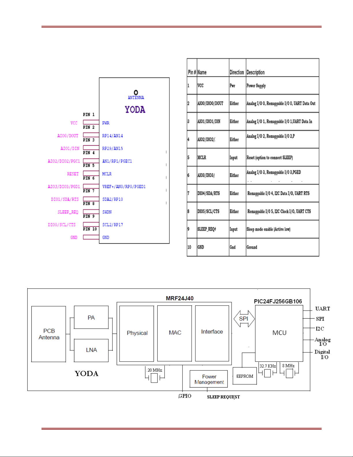
Pin diagram:
Pin Table:
10 pin Male Berg 2mm Pitch
Block Diagram:
Page 3 of 9 Si2 Micro Systems Pvt. Ltd. www.si2micro.com
Page 4

YYOODDAA
Module Overview:
YODA is a 2.4 GHz IEEE Std. 802.15.4™
compliant, module with integrated PIC micro
controller, crystal, internal voltage regulator,
matching circuitry, Power Amplifier, Low
Noise Amplifier and PCB antenna. The Module
operates in the non-licensed 2.4 GHz frequency
band. The integrated module design frees the
integrator from extensive RF and antenna
design, and regulatory compliance testing,
allowing quicker time to market.
The module is compatible with Microchip’s
ZigBee®, MiWi™ and MiWi P2P software
stacks.
SLEEP MODE: The module has sleep request
pin. Active low signal on this pin makes the
device on sleep mode. The pin needs to tie to
VDD if not used.
PIC POWER-SAVING TECHNOLOGY
The MCU of the module incorporate a range of
features that can significantly reduce power
consumption during operation. Key items:
• On-the-Fly Clock Switching: The device
clock can be changed under software control to
the Timer1 source or the internal, Low-Power
RC Oscillator during operation, allowing the
user to incorporate power-saving ideas into their
software designs.
• Doze Mode Operation: When timing-
sensitive applications, such as serial
communications, require the uninterrupted
operation of peripherals, the CPU clock speed
can be selectively reduced, allowing incremental
power savings without missing a beat.
• Instruction-Based Power-Saving Modes:
The microcontroller can suspend all operations,
or selectively shut down its core while leaving
its peripherals active, with a single instruction in
software.
Other Special Features of MCU:
• Peripheral Pin Select: The Peripheral Pin
Select (PPS) feature allows most digital
peripherals to be mapped over a fixed set of
digital I/O pins. Users may independently map
the input and/or output of any one of the many
digital peripherals to any one of the I/O pins.
• Communications: The PIC incorporates a
range of serial communication peripherals to
handle a range of application requirements.
There are three independent I2C modules that
support both Master and Slave modes of
operation. Devices also have, through the
Peripheral Pin Select feature, UARTs with builtin IrDA encoder/decoders and SPI modules.
• Analog Features: A 10-bit A/D Converter
module and a triple comparator module. The
A/D module incorporates acquisition time,
allowing for a channel to be selected and a
conversion to be initiated without waiting for a
sampling period, as well as faster sampling
speeds. The comparator module is configurable
for a wide range of operations.
• CTMU Interface: In addition to their other
analog features, MCU include the brand new
CTMU interface module. This provides a
convenient method for precision time
measurement and pulse generation, and can
serve as an interface for capacitive sensors.
• Parallel Master/Enhanced Parallel Slave
Port: One of the general purpose I/O ports can
be reconfigured for enhanced parallel data
communications. In this mode, the port can be
configured for both master and slave operations,
and supports 8-bit and 16-bit data transfers with
up to 16 external address lines in Master modes.
• Real-Time Clock/Calendar: This MCU
implements a full-featured clock and calendar
with alarm functions in hardware for use of the
core application.
Integrated Oscillators:
Integrated 8MHz crystal (connect to primary)
and 32.7 KHz crystal (connect to secondary)
used for MCU. Another integrated 20 MHz
crystal connects to the RF section.
Page 4 of 9 Si2 Micro Systems Pvt. Ltd. www.si2micro.com
Page 5

YYOODDAA
FCC Compliance Statements
This device complies with Part 15 of the FCC
Rules.
Operation is subject to the following two
conditions:
(1) This device may not cause harmful
interference, and
(2) This device must accept any interference
received, including interference that may
cause undesired operation.
NOTE: This equipment has been tested and
found to comply with the limits for a Class B
digital device, pursuant to part 15 of the FCC
Rules. These limits are designed to provide
reasonable protection against harmful
interference when the equipment is operated
in a commercial environment. This equipment
generates, uses, and can radiate radio
frequency energy and, if not installed and
used in accordance with the instruction
manual, may cause harmful interference to
radio communications. Operation of this
equipment in a residential area is likely to
cause harmful interference in which case the
user will be required to correct the
interference at his own expense.
The OEM integrator is still responsible for
testing their end-product for any additional
compliance requirements required with this
module installed (for example, digital device
emissions, PC peripheral requirements, etc.).
To meet FCC requirements, the following
settings were used.
The tranceiver MRF24J40 transmit power setting
(RFCON3 0x203) was -10dB.
Only channels 11 through 25 were selected.
The integrator of the module will not have
access to change any of the above settings.
Product Photos
CAUTION: Any changes or modifications not
expressly approved by the party responsible
for compliance could void the user’s authority
to operate the equipment.
This equipment should be installed and
operated with minimum distance 20 cm
between the radiator & your body.
End Product Labeling
This Module is labeled with its own FCC ID. If
the FCC ID Certification Number is not visible
while installed inside another device, then th e
device should display the label on it referring
the enclosed module. In that case, the final
end product must be labelled in a visible area
with the following:
“Contains Transmitter Module FCC ID:
2AAGG-YODA2P1”
OR
“Contains FCC ID: 2AAGG-YODA2P1”
The OEM should not provide information to
the end user regarding installation or removal
of this RF module or change RF related
parameters in the user manual of the end
product.
TOP
Page 5 of 9 Si2 Micro Systems Pvt. Ltd. www.si2micro.com
Page 6

YYOODDAA
Bottom
Electrical Characteristics
RECOMMENDED OPERATING CONDITIONS
Parameters Min Typ Max Units
Ambient Operating Temperature -40 — 85 °C
Supply Voltage (VDD) 3.0 — 3.6 V
Input High Voltage (VIH) 0.5 x VDD — VDD + 0.3 V
Input Low Voltage (VIL) -0.3 — 0.2 x VDD V
CURRENT CONSUMPTION
(TA = 25°C, VDD = 3.3V)
Chip Mode Condition Min Typ Max Units
Sleep Mode 1 uA
TX Maximum Output Power 20dB 120 150 mA
RX TBD 130 mA
CAPACITIVE LOADING REQUIREMENTS ON OUTPUT PINS
Parameters Condition Min Typ Max Units
All I/O pins EC mode. — — 50 pF
SCL, SDA In I2C mode. — — 400 pF
ADC SPECIFICATION
Parameters Condition Min Typ Max Units
Reference Voltage High AVSS + 1.7 — AVDD V
Reference Voltage Low AVSS — AVDD – 1.7 V
Absolute Reference Voltage AVSS – 0.3 — AVDD + 0.3 V
Absolute Input Voltage AVSS – 0.3 — AVDD + 0.3 V
Impedance for Analog Voltage
Source
Resolution — 10 — bits
10-bit — — 2.5K ohm
VINL = AVSS = VREFL =
Gain Error
Offset Error
0V, AVDD = VREFH = 3V — ±1 ±3 LSb
VINL = AVSS = VREFL =
0V, AVDD = VREFH = 3V — ±1 ±2 LSb
ADC CONVERSION TIMING REQUIREMENTS
Parameters Condition Min Typ Max Units
Conversion Time — 12 — TAD
Throughput Rate AVDD > 2.7V — — 500 ksps
Sample Time — 1 — TAD
Page 6 of 9 Si2 Micro Systems Pvt. Ltd. www.si2micro.com
Page 7

SLEEP MODE CHARACTERISTICS
Parameters Condition Min Typ Max Units
OFF State Leakage Current VIN = 3.3V, VEN = 0V 50nA 1 μA
Turn-On Delay Time VIN = +3.3V, ID = –100mA 0.85 1.5 μs
Turn-On Rise Time VIN = +3.6V, ID = –100mA 0.5 1 5 μs
Turn-Off Delay Time VIN = +3.6V, ID = –100mA 100 200 ns
Turn-Off Fall Time VIN = +3.6V, ID = –100mA 60 100 ns
RF RECEIVER AC CHARACTERISTICS
Typical values are at TA = 25°C, VDD = 3.3V, LO Frequency = 2.445 GHz
Parameters Condition Min Typ Max Units
Compatible toIEEE
RF Input Frequency
RF Sensitivity — `-102 — dBm
Maximum RF Input -23 — — dBm -23 — — dBm
LO Leakage
Input Return Loss -8 -12 — dBm
Noise Figure (including matching) — 1.9 — dBm
Adjacent Channel Rejection @ +/-5 MHz 30 — — dBm
Alternate Channel Rejection @ +/-10 MHz 40 — — dBm
RSSI Range 50 — dBm
RSSI Error -5 5 dBm
Std. 802.15.4
Measured at Balun
Matching Network
Input at
Frequency,2.405-2.48
GHz
2.405 — 2.48 GHz
— -60 — dBm
RF TRANSMITTER AC CHARACTERISTICS
Typical values are at TA = 25°C, VDD = 3.3V, LO Frequency = 2.445 GHz
Parameters Condition Min Typ Max Units
RF Carrier Frequency 2.405 — 2.475 GHz
Maximum RF Output Power — +10dBm — dBm
RF Output Power Control Range — 56 — dB
YYOODDAA
TX Gain Control Resolution — 1.25 — dB
Carrier Suppression — -30 — dB
Offset Frequency
> 3.5 MHz, at 0
dBm Output
TX Spectrum Mask for O-QPSK Signal
TX EVM — 15 — %
Power -33 — — dB
Page 7 of 9 Si2 Micro Systems Pvt. Ltd. www.si2micro.com
Page 8
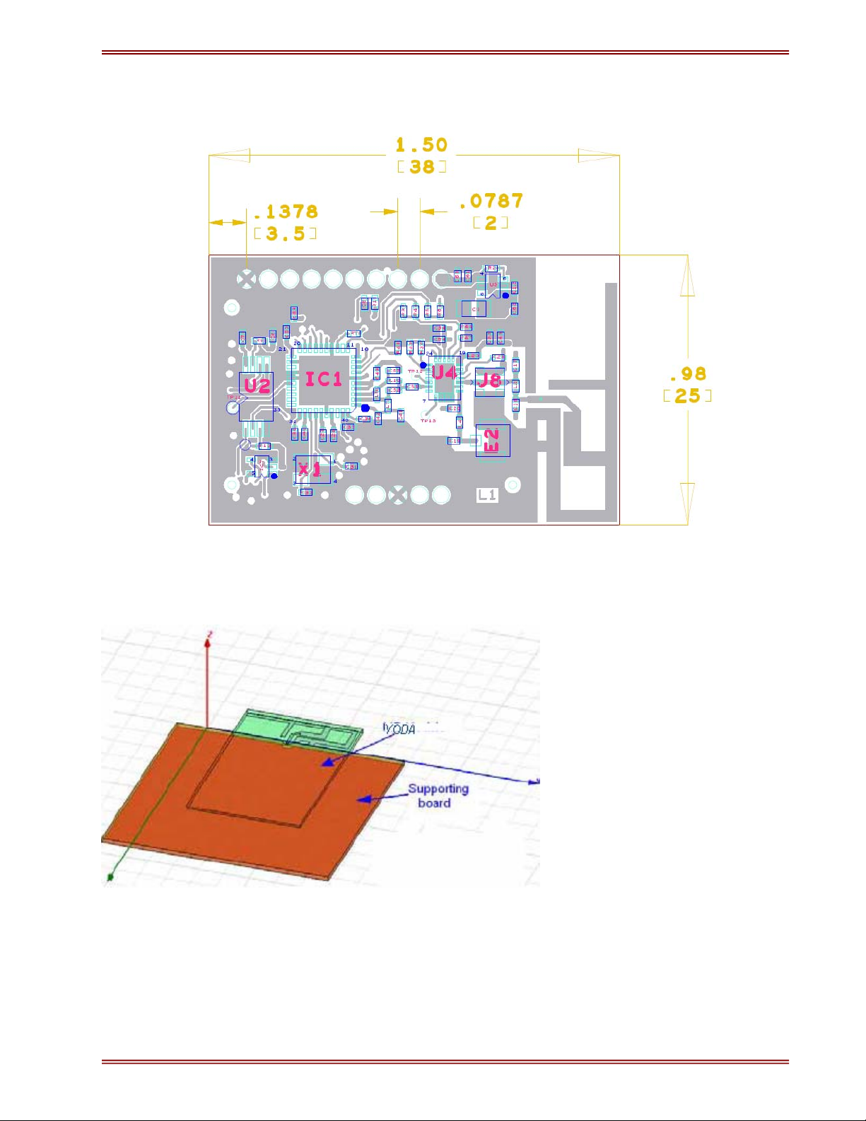
Module mounting details:
Foot print
PCB Antenna simulation setup / drawing
YYOODDAA
Page 8 of 9 Si2 Micro Systems Pvt. Ltd. www.si2micro.com
Page 9

Simulated 3D radiation pattern
YYOODDAA
Notes:
Page 9 of 9 Si2 Micro Systems Pvt. Ltd. www.si2micro.com
 Loading...