

Page 1
Shure Incorporated
222 Hartrey Avenue
Evanston IL 60202-3696 U.S.A.
T Wireless System
SERVICE MANUAL CHANGE NOTICE
T4 DIVERSITY RECEIVER
Changes and c orrections h ave b een m ade t o t he S ervice M anual f or t he T 4 R eceiver . To u pdate y our S ervice
Manual, remove the pages identif ied in the tables belo w and replace them with the pages attached to this
Change Notice. Note that there are no changes to pages not specif ically identif ied in the tables below.
T4 RECEIVER SERVICE MANUAL REVISION HISTORY
Release Part Number Date Code Color
Original 25A1020 QG White
Revision 1 25B1020 SB Pink
Revision 2 25C1020 SI White
Revision 3 25C1020 TF White
Revision 4 25C1020 CC White
Revision 5 25C1020 EA Red
CHANGES EFFECTIVE JANUARY 13, 2005
REMOVE
these pages from the
T4 Service Manual
21 & 22 21 & 22
INSERT
these new Revision pages into the
T4 Service Manual
E1999, Shure Incorporated Printed in U.S.A.
25–1020–1 (EA)
Page 2
Characteristics
ÁÁÁ
ÁÁÁ
Á
Á
ÁÁÁ
Á
Á
Á
Á
Á
ÁÁÁ
Á
ÁÁÁ
ÁÁÁÁ
Á
Á
General
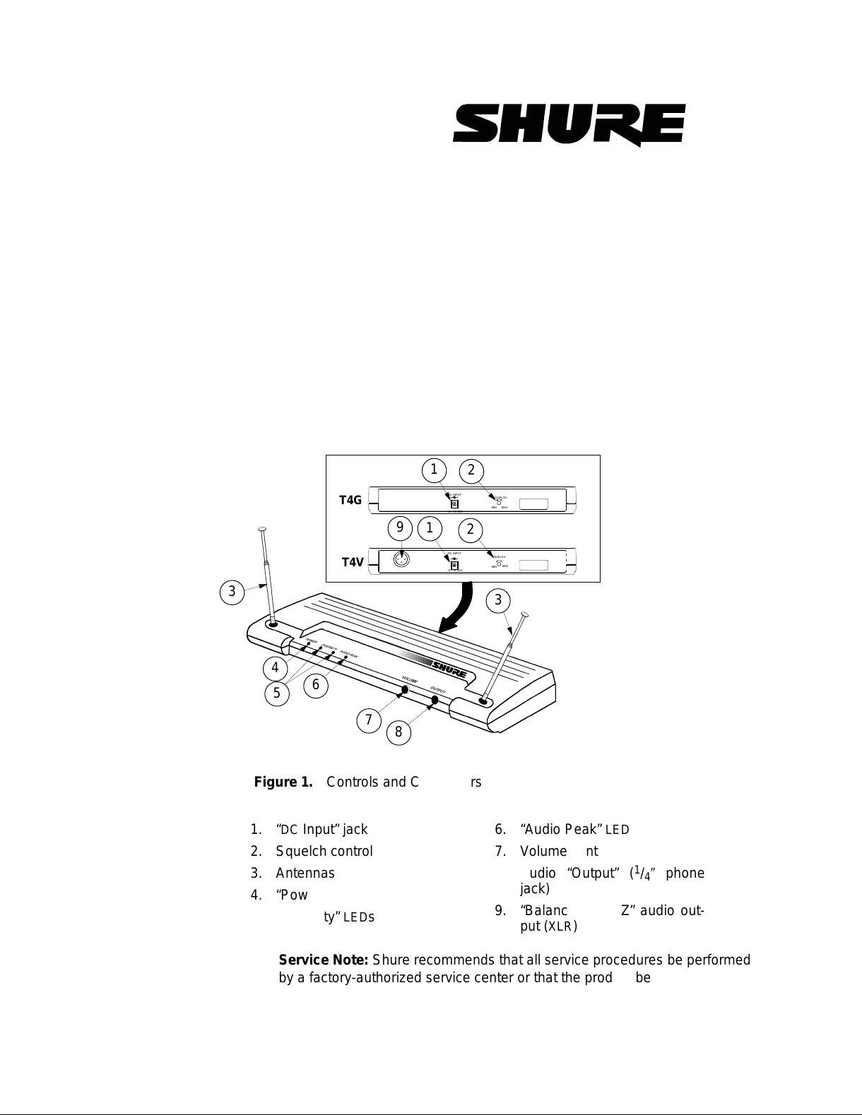
This manual tells how to service and align the Shure T4 Diversity Receiver
(Figure 1). This single-channel, crystal-controlled unit operates within the
169 MHz to 238 MHz VHF-FM band.
3
®
Service Manual
25C1020 (EA)
T4 Diversity Receiver
1
2
T4G
T4V
9
DC INPUT
12-18 VDC
1
DC INPUT
12-18 VDC
2
SQUELCH
MIN
SQUELCH
MIN
3
MAX
MAX
E1999, Shure, Inc.
Printed in U.S.A.
25C1020 (EA)
4
6
5
7
8
Figure 1. Controls and Connectors
1. “DC Input” jack
2. Squelch control
3. Antennas
4. “Power” LED
5. “Diversity” LEDs
6. “Audio Peak” LED
7. Volume control
8. Audio “Output” (1/4Ȃ phone
jack)
9. “Balanced Low Z” audio output (XLR)
Service Note: Shure recommends that all service procedures be performed
by a factory-authorized service center or that the product be returned directly
to Shure Brothers Inc.
1 Characteristics
Page 3

Shure T4 Diversity Receiver
Circuit Description
The Shure Model T4 is a single-conversion superheterodyne diversity FM
receiver operating in the 169–238 MHz band. It is intended for use with the
matching Shure T Series wireless transmitters.
RF Stages
Two complete, independent RF sections provide diversity reception. Signals
enter via the single-element, quarter-wave antennas.
Channel A: The signals pass through a double-tuned filter (L3 and L4) before entering MOSFET amplifier Q1. The output of this stage is double-tuned by
L5 and L6, which also provide impedance-matching to Gate 2 of GaAs MESFET
(gallium arsenide metal semiconductor field effect transistor) mixer Q3. Gate 1
receives the local oscillator signal from transistor Q5. A third-overtone quartz
crystal in the 50–70 MHz range provides frequency control. The collector circuit
of the oscillator is tuned by L8 to the third harmonic of the crystal (160–230 MHz)
to provide the proper injection frequency for a 10.7 MHz intermediate frequency
(IF).
Channel B: This channel is identical in design to channel A. The signals
from the antenna pass through a double-tuned filter (L12 and L13) before entering MOSFET amplifier Q6. The output of this stage is double-tuned by L14 and
L15 and fed to Gate 2 of GaAs MESFET mixer Q8. Gate 1 receives the local oscillator injection from buffer transistor Q4, which is tuned by L7. The buffer stage
helps isolate the diversity channels from one another by preventing crosstalk
through the common local oscillator section.
IF and Audio-Detection Stages
Channel A: L2 tunes the output of mixer Q3 to 10.7 MHz before the signal
enters ceramic filter FL3. Transistor Q2 provides IF amplification to make up for
the losses in the filters. After passing through a second IF filter, FL2, the signal
enters amplifier/detector U1. The detected audio from pin 6 is amplified by
U105C.
Channel B: L11 tunes the output of mixer Q8 to 10.7 MHz before the signal
enters ceramic filter FL6. Transistor Q7 provides IF amplification before the signal
passes through the second ceramic filter, FL5, and enters amplifier/detector U2.
The detected audio from pin 6 is amplified by U108B.
Noise-Operated Squelch
A noise-operated squelch system provides both diversity-channel selection
and muting. Noise signals are obtained from the additional detector outputs at
pin 7 of U1 and U2.
Noise Signals
Channel A: The squelch level control (R16) adjusts the noise signal from U1
before it is amplified by U105A. Active high-pass filter UI05D removes audio
components that could cause false triggering. The noise is then rectified by D101
and smoothed by C111 to provide a dc voltage that varies with the amount of
noise present on the detected signal.
2Characteristics
25C1020 (EA)
Page 4

Shure T4 Diversity Receiver
Channel B: This follows an identical scheme: noise signals from U2 are adjusted by squelch level control R41 before being amplified by U108C, filtered by
U108A, rectified by D107, and smoothed by C140.
Comparator Circuits
U106C and U106D compare the dc noise signals from the two channels.
When these signals are comparable, U106C and U106D direct analog switches
U103C (Channel A) and U103B (Channel B) to allow both channels to pass
through. The signals from each channel are correlated while the noise is uncorrelated, which makes possible a theoretical signal-to-noise improvement of 3 dB.
When the dc noise signals are not comparable, the channel with less noise is
chosen.
U106A imposes an additional criterion on Channel A, and U106B does the
same for Channel B. Each channel’s dc noise voltage is compared to a threshold
set by user-adjustable R112 (Squelch). A channel whose noise exceeds this
threshold is squelched. If both channels exceed their thresholds, the audio output of the receiver is squelched. Squelching is accomplished by tying together
the outputs of U106A and U106C (Channel A) or U106B and U106D (Channel
B). These outputs also control the yellow “Diversity” status indicators. Comparator U102 provides additional attenuation in the squelched state by shutting off
compandor U3.
Audio Output
“Peak” LED
Power
The audio signals from the two channels pass through analog switches
U103C and U103D, are buffered by U109A, and enter U3, which provides a 2:1
logarithmic expansion. An additional IC amplifier (U109D) operates in conjunction
with U3 to provide a lower noise floor. The output of this stage passes through
the Volume control (R126) to the “Output” connector (J101). A bridging amplifier
formed by U109B and U109C provides the “Balanced Low Z” output.
This red indicator warns the user when the transmitter deviation is approaching the limit of 15 kHz. This function is implemented by a window comparator
(U102C and U102D) and a pulse stretcher (U102B) that makes short transients
more visually apparent.
The green “Power” LED indicates when the external power converter (or a
battery pack) is supplying power to the receiver. The circuitry operates normally
with an input of 12–18 Vdc. D10 provides reverse polarity protection, and U101
supplies voltage regulation. The “Dc Input,” audio “Output,” and “Balanced
Low Z” output connectors are filtered to prevent local oscillator radiation from the
cables.
25C1020 (EA)
3 Characteristics
Page 5

Shure T4 Diversity Receiver
Notes
4Notes
25C1020 (EA)
Page 6

Preliminary Tests
Listening Tests
Before disassembling the unit, operate it to determine whether it is functioning normally. First and most important: Review the customer’s complaint (if available) and focus your tests on the problem. If this proves inconclusive or you want
somewhat more extensive checks, perform the following functional tests.
Functional Tests
The following tests require partial disassembly of the unit:
RF Test
The following is the best “fast” test of a receiver’s RF performance. A receiver that passes this test can be removed from the list of suspects for any “dropout” or “range” problem.
Initial Set-up
1. Set the receiver’s Squelch control to its middle position and the Volume
control to its maximum position.
Shure T4 Diversity Receiver
Audio Tests
2. Set the RF signal generator to the receiver’s frequency.
3. Remove the receiver’s antenna (see “Disassembly,” page 7). Plug the
BNC end of the 50 Ω test cable into the RF signal generator. Tack-solder
the cable’s center conductor to the receiver’s antenna input (TPA1 or
TPB1), and the shield to a ground plane as close as possible to the an-
tenna input (TPA2 or TPB2).
Test
1. Connect power to the receiver and turn it on.
2. Verify that the unit unsquelches with RF signals greater than –89 dBm.
3. When the unit unsquelches, verify that the “Diversity” LED glows.
Initial Set-up
1. Set the RF generator as follows:
Level: –60 dBm
Deviation: 15 kHz
Modulation: Ext
2. Set the audio analyzer as follows:
25C1020 (EA)
Amplitude: 1.4 V
Frequency: 1 kHz
3. Using a 3.3 kΩ load, connect the receiver’s unbalanced audio output to
the input of the audio analyzer, and engage the 400 Hz and 30 kHz fil-
rms
5 Preliminary Tests
Page 7

Shure T4 Diversity Receiver
ters. The receiver’s Volume control should still be in its maximum position.
Tests
1. Verify the following receiver measurements:
Units that Pass
S Audio level is 400 mV
reference level for the next two steps.
S Thd is <0.75%.
2. Change the audio analyzer’s frequency to 100 Hz, and disengage the
audio analyzer’s 400 Hz filter. Verify that the receiver’s unbalanced audio
output is within +2 dB, –1 dB of the reference level recorded in step 1.
3. Set the audio analyzer’s frequency to 10 kHz. Verify that the receiver’s
unbalanced audio output is –7.5 dB to –10.5 dB of the reference level
recorded in step 1.
4. Model T4V only: Place a 150 Ω load across the receiver’s balanced output, then connect this output to the audio analyzer. Verify that the output
is 65 mV
5. If you are finished testing the receiver, remove the test cable and reinstall the antenna (see “Reassembly,” page 8).
If the receiver passes these tests, then it is functioning as expected and
shouldn’t require alignment. If you did not use the customer’s microphone transmitter for these tests, check it for proper operation. If it also checks out of it it was
not sent in with the receiver, inform the customer that the product has retested
within specifications.
, "15 mV. Remove the 150 Ω load.
rms
, "90 mV. Record your measurement as a
rms
6Preliminary Tests
25C1020 (EA)
Page 8
Shure T4 Diversity Receiver
Disassembly and Assembly
To access the printed circuit (pc) board, disassemble the receiver.
CAUTION
Observe precautions when handling this static-sensitive device.
Disassembly
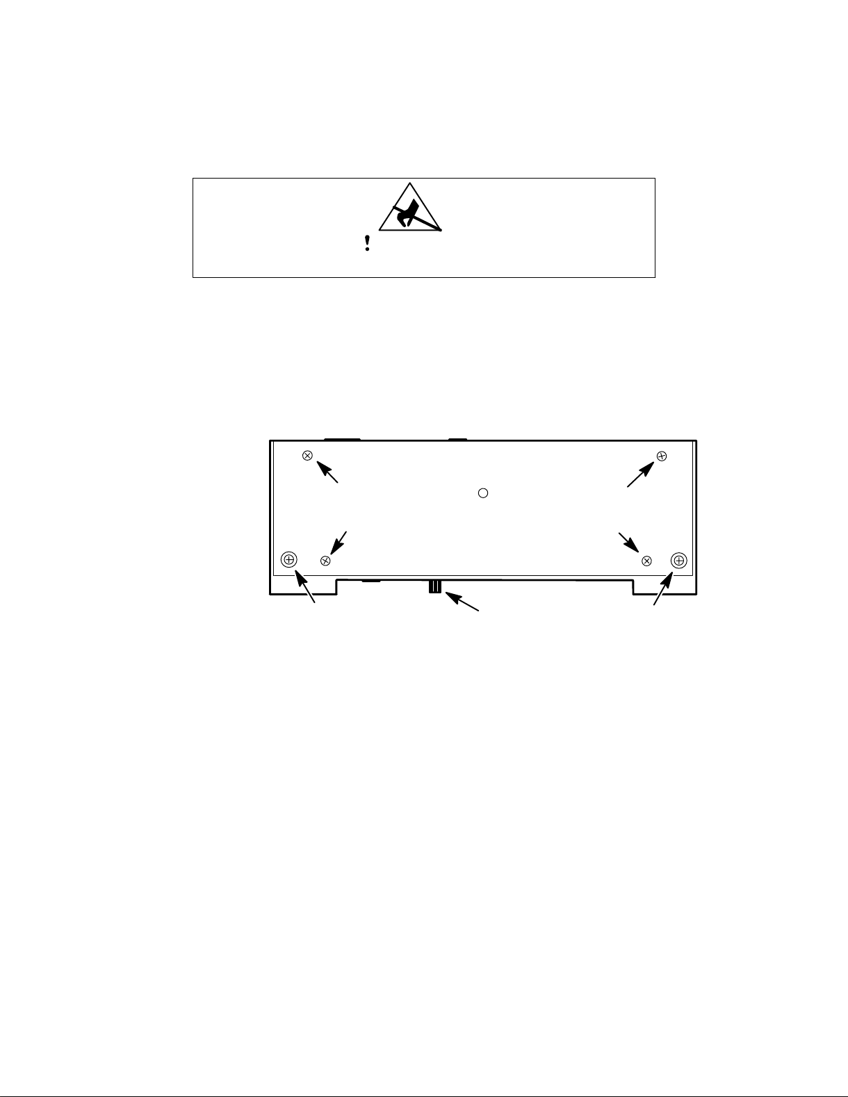
1. Disconnect all power to the receiver.
2. Collapse the antennas and rotate them until they lie flat against the case.
Place the receiver upside down. Remove and set aside the four screws
securing the bottom of the case (Figure 2).
Case
mounting
screws
Antenna
mounting
screw
Figure 2. Bottom View of Case
3. Place the receiver in its normal operating position and rotate the antennas to their vertical positions. Note that an adhesive-backed nameplate
at the at the rear of the unit holds the upper and bottom parts of the case
together. To open the case, carefully separate the upper part from the
bottom part at the front of the unit. Carefully swing the bottom part of the
case away until the two halves are at a 90° angle, to allow removal of the
circuit board and antennas (Figure 3).
4. After the circuit board has been removed, pull off and retain the Volume
knob.
Volume knob
Case
mounting
screws
Antenna
mounting
screw
25C1020 (EA)
7 Disassembly and Assembly
Page 9
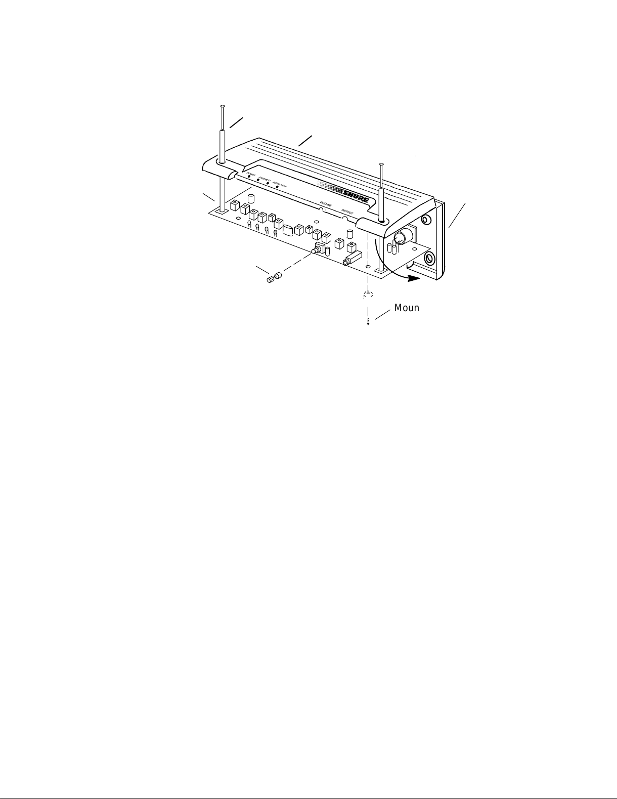
Shure T4 Diversity Receiver
Circuit
board
Volume knob
Antenna
Case top
Case bottom
Mounting screw
Figure 3.
Reassembly
1. Slide the Volume knob back on: note how it is keyed to the flat part of the
shaft.
2. Rotate the antennas to their vertical positions. Place the pc board, component-side up, inside the top half of the case: after feeding the antennas through their holes, make sure the notches in the case align with the
Volume knob, the LEDs align with the holes in the upper half of the case,
and that the board is fully seated on the studs.
3. Swing the two halves of the case together until they snap in place.
4. Rotate the antennas until they lie flat against the case. Turn the receiver
upside down and secure the assembly with the four screws removed
earlier (Figure 2, page 7). Check that the Volume knob rotates freely.
Antenna Replacement
The antennas can be replaced without disassembling the case. Rotate the
antenna you are replacing to its vertical position, collapse it, and remove the
mounting screw through its access hole in the bottom of the case (Figure 2). Insert the new antenna and start the screw from the bottom, leaving it loose
enough for you to rotate the entire antenna between your fingers. Rotate the antenna in this way as you lightly press it into the case until you feel the base seat
in the slot of the bracket on the pc board. Tighten the screw.
8Disassembly and Assembly
25C1020 (EA)
Page 10

Service Procedures
Reference Material
The Shure Wireless System T Series User’s Guide provides a description of
the unit as well as operating instructions, troubleshooting suggestions, and technical data.
Special Equipment and Tools
In addition to the standard items described in the Service Equipment manual,
you will need:
S a wireless microphone with the same frequency (usually a T1, T2, or
T11) to verify that the receiver is working properly
S an audio amplifier with a high-impedance input (w10 kΩ) and a
monitor speaker, for listening tests
System Operating Frequencies
Each receiver’s circuit board has a resistor next to the group letter (A–H,
J–L) that identifies the range of frequencies on which the receiver can operate
(see Figure 4). Table 1 shows the Group Letter and its associated frequencies.
Note that this chart applies only to T4 receivers.
Shure T4 Diversity Receiver
Table 1
Pc Board Groups
Group Frequency Range
A 169.000–173.975 MHz
B 174.000–179.975 MHz
C 180.000–185.975 MHz
D 186.000–191.975 MHz
E 192.000–197.975 MHz
F 198.000–203.975 MHz
G 204.000–209.975 MHz
H 210.000–215.975 MHz
J 216.000–222.975 MHz
K 223.000–229.975 MHz
L 230.000–237.975 MHz
Tables 2 and 3 provide information for identifying the system frequency. The
Crystal Code, together with the appropriate Shure model number, identifies a
specific operating frequency for transmitters and receivers. Note that, although a
Crystal Code always designates a specific frequency, it may be used with different Group Letters on other products.
25C1020 (EA)
9 Service Procedures
Page 11

Shure T4 Diversity Receiver
FCC-Approved Operating Frequencies
ETSI-Approved Operating Frequencies
Table 2
Group Crystal Code Freq. (MHz)
A V 169.445
A W 171.845
B CA 176.200
B CC 177.600
C CE 182.200
C CF 183.600
D CG 186.200
E CL 192.200
F CQ 202.200
G CV 208.200
Table 3
Group Crystal Code Freq. (MHz)
A AQ 173.800
B AY 174.100
B AZ 174.500
B ZZ 174.500
B BA 174.800
B NB 175.000
B BB 175.000
B ND 176.600
B NE 177.600
C NH 182.000
C NK 183.600
C NL 184.600
C CS 184.800
C S 184.800
D NP 189.000
D NR 190.600
E NX 197.600
F NY 198.600
F NZ 200.350
F PU 201.650
F PB 203.000
G PD 204.600
J PP 217.000
J PR 218.600
J PS 219.600
L PV 232.825
L PX 233.125
L PY 234.625
L PZ 237.325
10Service Procedures
25C1020 (EA)
Page 12

Changing the Frequency
The operating frequency of the T4 Receiver may be changed within a specific group by changing the crystal on the pc board (for group information, see the
preceding section). Check the receiver for proper operation before attempting to
change its operating frequency. After installing the new crystal, perform the alignment procedures. Then run an operational test to ensure the receiver is functioning properly. Finally, update the label to show the new frequency and letter identification code.
Note: To ensure proper operation, obtain the crystal from Shure and verify
that it operates within the frequency range of the pc board. Since crystals are
marked with the nominal oscillating frequency, not with a letter code, you can
use the following equation to determine the frequency at which a receiver will
operate with a given crystal:
Carrier Frequency = (3 nominal crystal freq. in MHz) + 10.71
Alignment
The alignment steps must be done together, as a single, continuous procedure. Before beginning, be sure to do the setup described in the following subsection, “Test Conditions.”
Shure T4 Diversity Receiver
Test Conditions
The following are the standard test conditions for the T4 Receiver:
S With a #1 Phillips screwdriver, remove the antennas.
S Load the the unbalanced, audio output (J101) with a 3.3 kΩ resistor.
S For RF adjustments, connect a 33 kΩ resistor between ground and
the following points:
Channel A: TPA4 (pin 13 of U1)
Channel B: TPB4 (pin 13 of U2)
S Set the potentiometers as follows:
Volume (R126): Fully CW
Squelch (R112): Midrange
Audio level (R106 and R168): Midrange
Mute level (R16 and R41): Midrange
Test Cable
1. Obtain a 50 Ω coaxial cable for connecting the circuit boards to various
test equipment. (To construct this cable, see “50 Ω Test Cable Assembly”
in the Service Equipment manual.) Refer to Figure 4 for the locations of
the test points, controls, and tuning components.
25C1020 (EA)
2. Tack-solder the c able to the pc board as f ollows:
Channel A: Center conductor to the antenna input (TPA1) and shield to
ground (TPA2)
Channel B: Center conductor to the antenna input (TPB1) and shield to
ground (TPB2)
11 Service Procedures
Page 13

Shure T4 Diversity Receiver
Presettings
Most field units should already be tuned closer to the desired settings than
these approximations. However, you may need to preset units when you are
changing the frequency or an RF coil, or when an unskilled person has attempted
to retune them.
Minimum inductance occurs when the core is level with the top of the
can. Turning the core further counterclockwise or even removing it will
not appreciably affect the inductance.
Maximum inductance occurs when the core is about two turns less than
its full clockwise rotation—about 3.2 mm (1/8 in.) below the top of the
can. Never screw the core against the board.
The manufacturer’s setting of the two smaller, IF coils (L2 and L11) is close
to their ideal setting, so you generally would not preset them. For coils L3–L8
and L12–L15, refer to Table 2 or 3 (page 10) to determine where the desired frequency lies within the board’s group. For frequencies near the bottom of a group,
use the maximum-inductance settings; for frequencies near the top of the group,
use the minimum-inductance settings.
Display Check
1. Connect an external 12–15 Vdc supply to the dc input (J103). The green
“Power” LED should glow.
2. Check for 9 Vdc ("0.35) at TP9 (pin 3 of voltage regulator U101).
Test-Equipment Settings
1. Plug into the RF generator the BNC end of the 50 Ω cable you soldered
to the pcb (antenna and ground). Set the generator’s controls as follows:
S –20 dBm on the receiver’s operating frequency
S "15 kHz FM deviation with 1 kHz modulation
2. Activate the 400 Hz high-pass and 30 kHz low-pass filters on the audio
analyzer.
12Service Procedures
25C1020 (EA)
Page 14

Group designator
(see Table 1)
XLR audio output
connector (J102)
Note: Used only on
Presenter and Vocal
Artist models
C150
C145
R168
B
Shure T4 Diversity Receiver
Antenna B
TPB2
TPB1
U101
D108
D109
Phone jack
!/4-in. (J101)
Power input (J103)
Note: Use Shure
PS20 or PS20E
Squelch control
(R112)
U108
U109
U107
U103
TPB5
C48
TPB4
U3
(On earlier
units only.)
TPB7
TPA7
L108
Channel B
U2
U102
Channel A
U1
R41
L11
B
TP9
L2
A
TPA4
B
L13
B
L14
B
TPB3
Y100
TPA3
L12
B
C118
R126
L15
B
L7
B
L8
A
L6
A
L5
A
Edge of
case bottom
Volume control
Knob
Crystal (see
Tables 2 and 3)
“Audio Peak”
(red)
B
“Diversity” (
(yellow)
A
“Power” (green)
U104
RF)
Note: L107 and L108 are
not found on earlier units.
25C1020 (EA)
U106
TPB6
TPA6
R16
A
TP8
L107
TPA5
U105
Figure 4. Major Components
13 Service Procedures
C6
R106
L4
A
L3
A
A
TPA2
TPA1
Antenna A
Page 15

Shure T4 Diversity Receiver
Coil Adjustments
Each channel has to be adjusted separately.
A: Channel A RF and IF
1. Disconnect the power to the receiver. Mute Channel B by grounding
2. Adjust the signal generator’s RF output so that you obtain a reading of
3. Adjust coils L2, L8, L3, L5, L4, and L6 (in that order) for maximum volt-
TPB7 (pin 14 of U106). Reconnect the power.
approximately 2 Vdc at TPA4. If this is unattainable even with the full –20
dBm generator output, adjust IF coil L8 until you obtain a reading above
2 V. If you cannot get more than 1.25 V, return L8 to its preset position
and adjust coil L2.
age at TPA4. Use a hex tuning wrench for all adjustments except L2,
which requires a non-metallic screwdriver (like a Toray driver). Reduce
the generator output as required to keep the signal voltage under 3 Vdc.
Perform the final adjustments with a generator output of approximately
–85 dBm.
Note: For coils other than L2, the “sharpness” of the tuning depends on
the operating frequency within the frequency group. At the upper and
lower edges of a group, a distinct peak may be difficult to observe. In this
case, adjust the core for maximum indication.
B: Channel A Audio
Note: Before making the following adjustments, power up the circuit
board for at least one minute. This allows the FM detector to stabilize.
1. Set the RF signal generator for an output level of –60 dBm, a modulation
of 1 kHz, and a deviation of 15 kHz.
2. Version E and later boards only: With the probe of an ac voltmeter on
TPA5 (pin 8 of U105), adjust L107 for peak output.
3. Adjust R106 for 0 dBu (775 mV), "0.1 dB, at TPA5 (pin 8 of U105).
4. Reset the signal generator to its minimum output level (or “Off”). Check
that both ”Diversity” LEDs turn off.
5. Set the signal generator as follows:
Level: –50 dBm
Ext. Modulation: 50 kHz
Deviation: 15 kHz
Adjust R16 for 1 Vdc ("0.5 Vdc) at TPA6 (the positive end of C111).
6. Turn off the modulation of the signal generator. Set its output to the minimum level, then gradually increase the level until the “Diversity A” LED
turns on. This should occur with an RF input between –102 dBm and
–87 dBm (typically –95 dBm).
7. Disconnect power from the receiver. Remove the jumper from TPB7 and
the RF input from TPA1 and TPA2.
C: Channel B RF and IF
1. Make sure that the RF generator is connected to the antenna input for
Channel B. Mute Channel A by grounding TPA7 (pin 13 of U106).
14Service Procedures
25C1020 (EA)
Page 16

Shure T4 Diversity Receiver
2. Connect power to the receiver.
3. Adjust the RF output of the signal generator RF output so that you obtain
a reading of approximately 2 Vdc at TPB4. If this is unattainable even
with the full –20 dBm generator output, adjust IF coil L7 until you obtain a
reading above 2 V. If you cannot get more than 1.25 V, return L7 to its
preset position and adjust coil L11.
4. Adjust coils L11, L7, L12, L14, L13, and L15 (in that order) for maximum
voltage at TPB4. Use a hex tuning wrench for all adjustments except L11,
which requires a non-metallic screwdriver (like a Toray driver). Reduce
the generator output as required to keep the signal voltage under 3 Vdc.
Perform the final adjustments with a generator output of approximately
–85 dBm.
Note: For coils other than L11, the “sharpness” of the tuning depends on
the operating frequency within the frequency group. At the upper and
lower edges of a group, a distinct peak may be difficult to observe. In this
case, adjust the core for maximum indication.
D: Channel B Audio
Note: Before making the following adjustments, power up the circuit
board for at least one minute. This allows the FM detector to stabilize.
1. Set the signal generator for an output level of –60 dBm, a modulation of
1 kHz, and a deviation of 15 kHz.
2. Version E and later boards only: With the probe of an ac voltmeter on
TPB5 (pin 7 of U108), adjust L108 for peak output.
3. Adjust R168 for 0 dBu (775 mV), "0.1 dB, at TPB5.
4. Reset the signal generator to its minimum output level (or “Off”). Check
that both “Diversity” LEDs turn off.
Level: –50 dBm
Ext. Modulation: 50 kHz
Deviation: 15 kHz
5. Set the RF signal generator as follows:
Adjust R41 for 1 Vdc ("0.5 Vdc) at TPB6 (the positive end of C140).
6. Turn off the modulation of the signal generator. Set its output to the minimum position, then gradually increase the level until the “Diversity B”
LED turns on. This should occur with an RF input between –102 dBm
and –87 dBm (typically –95 dBm).
7. Disconnect power from the receiver. Remove the jumper from TPA7 and
the RF input from TPB1 and TPB2.
E: Final Steps
1. If you were unable to align the unit, refer to the “Bench Checks” section,
which follows immediately.
25C1020 (EA)
2. When you have finished working on the unit, reassemble it, as described
in the earlier “Reassembly” subsection on page 8.
15 Service Procedures
Page 17

Shure T4 Diversity Receiver
Bench Checks
Note: In this section, test points for Channel A are given first, and the corre-
sponding test points for Channel B are enclosed in square brackets.
DC Power
n Check for 9 Vdc (±0.35 Vdc) at TP9 (pin 3 of U101):
S If the voltage is lower than normal (but not zero): Check for 15 Vdc at the
input of U101 (pin 1), a reversed electrolytic capacitor (C152), or a stage
that is drawing excessive current.
S If the voltage is zero: Check for solder bridges or shorted foil traces (de-
fective pcb).
S If the voltage is higher than normal or the other tests prove negative: Re-
place U101.
n Check for 5 Vdc (±0.25 Vdc) at TP8 (pin 10 of U3).
Tuning
n First check that that the RF signal is being applied to the correct diversity
channel and that the other channel is being muted with the jumper.
n If the voltage reading at TPA4 [TPB4] does not vary when the RF coils are
adjusted, check the operation of the local oscillator. If everything is working
properly, you should obtain a reading of 1–2 Vdc with a –95 dBm RF input
signal, depending upon component parameters and receiver frequency. If
you do not obtain this reading, try the following:
S With the RF generator turned off, use a spectrum analyzer to measure
the injection level at TPA3 [TPB3] for approximately –15 to –20 dBm.
S If the preceding level is correct, use a frequency counter to verify that the
local oscillator signal is 10.7 MHz (±.015 MHz) below the operating frequency of the receiver.
Example: To receive 169.445 MHz, the local oscillator frequency
should be 158.745 MHz (±.015 MHz). Crystal Y100 operates at a
third of this frequency, or 52.915 MHz. The nominal crystal frequency, which is stamped on the part, is 3.333 kHz lower
(52.911667 MHz) in this example. This discrepancy arises because
the load reactance of the oscillator is not precisely zero.
n If any of the RF coils will not tune properly, check for frequency-dependent
capacitors that are missing or have the wrong value. If the IF coil will not
tune, check C9 [C52].
n If all the coils tune but the RF signal is low, compare the dc voltages and
components at RF amplifier Q1 [Q6] with those of a properly working unit.
Muting
n With TPA7 [TPB7] connected to ground, the selected diversity channel should
be squelched and the “A” [“B”] LED should be off, whether or not an RF input
16Bench Checks
25C1020 (EA)
Page 18

Audio
Shure T4 Diversity Receiver
signal is present. If you obtain different results, compare the dc voltages at
U106, U107 (earlier units only), U103, and U105 [U108] with those of a properly working unit, or replace the pc board.
n If the muting circuit works but has insufficient adjustment range, set the
generator for a –95 dBm signal and check TPA4 [TPB4] for 1–2 Vdc, as de-
scribed in the preceding, “Tuning,” subsection. If you get a lower reading,
consider the following:
S Low RF levels at the input of U1 [U2] will cause inadequate noise at the
output of U105D [U108A].
S In order for the noise squelch circuit to function, the detector portion of
U1 [U2] must also be functioning properly (see the following, “Audio,”
subsection).
S If necessary, check the component values and dc voltages (versus those
of a known working unit) of the following:
Noise amplifier U105A [U108C]
High-pass filter U105D [108A]
n If there is no audio at the output of the receiver:
S To verify that the receiver is not squelched, defeat the squelch circuit by
rotating R16 [R41] fully CCW. There should be 9 Vdc at TPA7 [TPB7],
and the yellow “A” [“B”] “Diversity” LED should be on.
S If the preceding test does not yield the proper results, check for a prob-
lem in the squelch circuitry (see the “Muting” subsection, immediately
above).
n Next, check pin 6 of U1 [U2] for an audio signal of approximately –15 dBV. If
there is no detected audio:
S Check C1 [C44] and the components connected to pins 7–10 of U1 [U2].
S On earlier units only: Make sure that FL1 [FL4] is an 86A8920 ceramic
discriminator and not an 86A8910 ceramic filter, which is similar in appearance.
S Check the dc voltages at U1 [U2] against those of a known working unit.
If no other problem is found, replace the IC.
S If audio is present at pin 6 of U1 [U2] but not at the output of the receiver,
trace the signal through signal amplifier U105C (TPA5) [U108B (TPB5)]
and expander U3/U109D. When measuring at audio TPA5 [TPB5], use a
1 kΩ resistor in series at the test point to prevent loading the amplifier.
S Check the Volume control (R126) and the components going to the au-
dio output jack (J101).
S On vocal models, check for a signal at the Low Z microphone-level out-
put, J102. If no signal is present, check U109B, U109C, and associated
components.
S Check the dc voltages on any stage that is not working properly; then
look for wrong or missing components. Replace the ICs in the faulty
stage if no other problem is found.
RF
25C1020 (EA)
17 Bench Checks
Page 19

Shure T4 Diversity Receiver
n If you cannot set the audio level properly with R106 [R168], make sure that
the other diversity channel is squelched: only one channel should be activated during this adjustment.
n If you can set the audio levels properly for each channel while the other is
squelched, but these levels change significantly when both channels are activated, check U103.
n If the audio level is correct but the unit exhibits high total harmonic distortion
(thd), vary the RF input frequency 20 kHz above and below the operating
frequency. If the thd drops to an acceptable level, check the local oscillator
frequency. If it is within specifications, repeak the quadrature coil, L107
[L108], for maximum ac output at TP5 [TP8] (see step 1 of “Channel A Audio,” page 14 [step 1 of “Channel B Audio,” page 15]). On earlier units only,
which do not have L107, replace ceramic discriminator FL1 [FL4].
n If the audio circuitry works properly but the red audio peak LED either fails to
light when the standard test signal is applied or remains on when there is no
modulation, check the dc voltages at U102B, U102C, and U102D against
those in a known working unit. Also check the peak LED itself. Replace any
defective components.
18Bench Checks
25C1020 (EA)
Page 20

Notes:
Shure T4 Diversity Receiver
25C1020 (EA)
19 Notes:
Page 21

Shure T4 Diversity Receiver
Replacement Parts and Drawings
On the next page, the parts are listed according to the designations from the
pc board (see Figure 5, page 25) and the schematics at the end of this manual.
Parts shown on the circuit diagram and not listed below are available through
electronic-parts distributors.
On the pages following the parts list are the drawings of the printed circuit
boards and the schematics.
Product Changes
This section briefly describes significant changes to the T4.
Op Amps: The older part for U105, U108, and U109 (manufactured by Raytheon) was replaced. No other component changes were involved.
“E” Revisions: These revisions of the pc boards temporarily changed the IF
detector, deleted U107, changed a number of resistors and capacitors, made
eight coils and a resistor frequency-dependent, and changed Q3 and Q8 from
bipolar mixers to GaAs MESFET (gallium arsenide metal semiconductor field-effect transistor) mixers.
FM Detector: A temporary shortage of the Sanyo chip caused the temporary
substitution of a Harris FM detector. It used two additional resistors, R174 and
R175. Should you replace the Harris detector with the Sanyo unit, be sure to remove those two resistors.
Frequencies: The “G” version of the pc board introduced many new European frequencies, five additional board groups (E–J), and a consequent reassignment of some frequencies to different board groups. The revised board received both some component changes and an altered layout.
Quadrature Coil: The extensive changes on the “G” pc boards, referred to
in the preceding paragraph, included the replacement of ceramic discriminators
FL1 and FL4 with quadrature coils L107 and L108.
Test Points: On earlier versions of the pc boards, the test points were designated as “TP1A,” “TP1B,” etc.; on newer boards, the designations are “TPA1,”
TPB1,” etc.
“J” Frequency Code: Starting in the summer of 1997, T Series transmitters
and receivers tuned to 175.000 MHz have been labeled as “BB” rather than “J.”
The change was made to avoid confusion with the different meaning of the “J”
designation in the LX88 and ELX88 units. It is only a labeling change; the units
are physically the same.
“L” Frequencies: The “F” pcb assembly mainly addresses the addition of a
new “L” group with new European frequencies. There were also a number of minor changes to capacitors, partly small corrections, mainly adaptations to simplify
parts procurement and stocking.
20Replacement Parts and Drawings
25C1020 (EA)
Page 22

Shure T4 Diversity Receiver
Parts Designations
The following comments apply to the parts list and the schematic:
Resistors: All resistors are surface-mount with 1/10 W rating and 1% toler-
ance.
Capacitors: Unless otherwise noted, non-polarized capacitors are surfacemount NPO dielectric types with a 100 V capacity and a 5% tolerance, and polarized capacitors are tantalum types.
Table 1
T4 Hardware Replacement Parts
Reference
Designation Description Shure Part No.
A1 Printed Circuit Board Assembly 90_8550F
[In the underlined space, insert the
proper Group Code-Letter from
Table 2 or 3, page 10.]
E1 Antenna 95A8320
K1 Case Screws, Antenna Mounts & Antenna
Screw Kit
Case Screw 30C1245A
Antenna Mount Bracket 53A8322
Antenna Screw 30C1208A
Hardware Kit 90VY1371
MP1 Case (top) 65B8198
MP2 Case (bottom) 65A8199
MP3 Knob (for Volume control) 65B8235
MP4 Screw, Hi–Lo, Pan (for case) 30C1245A
MP5 Nameplate, Polycarbonate, Rear (Euro) 39A8368
MP6 Nameplate, Polycarbonate, Rear (Domestic) 39B8368
RPW612
Table 2
T4 PCB Replacement Parts
Reference
Designation Description Shure Part No.
C6, 48 Capacitor, Electrolytic, 470uF, 16V, 20% 86S629
C105,114,144,
149,151,153
C111,116,127,
132,140,141,
C118,145,150 Capacitor, Electrolytic, 47uF, 63V, 20% 86BE629
C129 Capacitor, Electrolytic, SMD, 4.7uF, 35V,
C152 Capacitor, Electrolytic, SMD, 100uF, 16V,
25C1020 (EA)
Capacitor, Electrolytic, SMD, 10uF, 35V,
20%
Capacitor, Electrolytic, SMD, 1.0uF, 50V,
10%
156
20%
20%
151BF106MC
151BG105KB
151BF475MB
151BD107MD
21 Replacement Parts and Drawings
Page 23

Shure T4 Diversity Receiver
D101,107,110,
111,112,113
Diode, Signal, Switching, SOT–23, 100VDC
(MMBD7000L)
184A08
D108, 109 Rectifier, Silicon, 140VDC 184A20
FL2, 3, 5, 6 Ceramic Filter, 10.7MHz 86A8910
J101 Phone Jack, Stereo, Right Angle,
1
-inch 95A8329
/4
J102 XLR connector (Vocal units only) 95A8400
J103 DC Power Jack 95A8328
L1,10,101,102
Ferrite Bead, SMD 805, 600 OHM 162A12
,103,104,105,
106
L2, L11 If Coil, 4.7uH 82A8005
L7, 8 Tunable, 10 mm, RF Coil, Red, 45nH 82A8003
L9 Inductor, SMD 1008, .22uH (220nH) 162C06
L107, 108 Quadrature Coil, 10.7MHz 82A8004
Q1, 6 MOSFET (metal-oxide-semiconductor field-
183A23
effect transistor) SOT–143, (3SK131)
Q2, 4, 5, 7 Transistor, UHF/VHF, RF, SOT–23, NPN,
183A03
(MMBTH10L)
Q3, 8 Amplifier, 2 Gate, Hi Gain, Lo Noise, SOT143
183A12
(3SK177)
R16, 41, 106,
Potentiometer, Linear Taper 5 kΩ 46C84
168
R112 Potentiometer, Linear Taper, 100 kΩ
46A8008
(Squelch)
R126 Potentiometer, Log Taper, 10 kΩ (Volume) 46A8046
U1, U2 Integrated Circuit, FM IF, SO–16 (LA1235) 86A8877
U3 Compandor, SOL–16 (SA571D) 188A01
U101 9 V Regulator (MC7809CT) 86A8944
U102, 106 Comparator, Quad, Low Power, SO–14
188A123
(LP339M)
U103 Switch, Multiplexer, Quad, SO–14
188A19
(HEF14066)
U104 LED Bar, Green/Yellow/Yellow/Red 95A8519
U105,108,109 Quad Op Amp, SO–14 (MC33179D) 188A49
Y100 Crystal 40_8003A
[In the underlined space, insert the
appropriate Crystal Code from
Tables 2 and 3, p. 10]
Note: The tables on the following pages list frequency-dependent parts.
22Replacement Parts and Drawings
25C1020 (EA)
Page 24

Shure T4 Diversity Receiver
In the following four-part table, “Grp” is the board’s frequency group, and “Desig” is the number of the
resistor that designates the Group Number. The parts are listed across the tables in alphanumeric order.
All capacitor tolerances are in picofarads.
Table 3
Frequency-Dependent Parts I
Grp Desig C8, C51 C10 C11 C12, C56 C17
A R210 Not used 1 pF (0.1) 12 pF 18 pF 15 pF Not used
B R211 1 pF (0.1 ) Not used 12 pF 15 pF 12 pF 1.8 pF (0.1)
C R212 Not used 1 pF (0.1) 10 pF 15 pF 12 pF 1 pF (0.1)
D R213 1.8 pF (0.1) NA 10 pF 12 pF 12 pF Not used
E R214 1 pF (0.1) 1 pF (0.1) 20 pF 12 pF 10 pF 1 pF (0.1)
F R215 Not used Not used 20 pF 12 pF 10 pF Not used
G R216 Not used Not used 18 pF 10 pF 10 pF Not used
H R217 1 pF (0.1) 1.8 pF (0.1) 15 pF 8.2 pF 8.2 p
F
J R218 1 pF (0.1) 1.8 pF (0.1) 15 pF 18 pF 15 pF 1.8 pF (0.1)
K R219 Not used 1 pF (0.1) 15 pF 18 pF 15 pF 1.8 pF (0.1)
L R220 1 pF (0.1) 1.8 pF (0.1) 12 pF 15 pF 15 pF Not used
C18
1 pF (0.1)
Frequency-Dependent Parts II
Grp C19, C63 C20 C21 C33, C36
A 56 pF 12 pF NA 15 pF 20 pF 20 pF 1 pF (0.1)
B 56 pF 10 pF 1 pF (0.1) 15 pF 20 pF 20 pF NA
C 56 pF 10 pF NA 12 pF 20 pF 20 pF 1 pF (0.1)
D 56 pF 8.2 pF (0.25) 1 pF (0.1) 12 pF 20 pF 20 pF NA
E 56 pF 8.2 pF (0.25) 1 pF (0.1) 10 pF 20 pF 20 pF 1 pF (0.1)
F 56 pF 8.2 pF (0.25) NA 10 pF 20 pF 20 pF NA
G 47 pF 6.8 pF (0.25) NA 8.2 pF (0.25) 20 pF 20 pF NA
H 47 pF 5.6 pF (0.25) 1 pF (0.1) 10 pF 20 pF 20 pF NA
J 56 pF 15 pF 1 pF (0.1) 6.8 pF (0.25) 10 pF 10 pF NA
K 56 pF 15 pF NA 6.8 pF (0.25) 10 pF 10 pF 1 pF (0.1)
L 56 pF 12 pF 1.8 pF (0.1) 5.6 pF (0.25) 10 pF 27 pF 1 pF (0.1)
C40 C42 C54
25C1020 (EA)
23 Replacement Parts and Drawings
Page 25

Shure T4 Diversity Receiver
Frequency-Dependent Parts III
Grp C55 C60 C61
C64
C65
C77, C78
A 12 pF 15 pF 1 pF (0.1) 12 pF Not used 3.3 pF (0.1)
B 12 pF 15 pF Not used 10 pF 1 pF (0.1) 3.3 pF (0.1)
C 10 pF 12 pF 1.8 pF (0.1) 10 pF NA 1.8 pF (0.1)
D 10 pF 12 pF 1 pF (0.1) 8.2 pF (0.25) 1 pF (0.1) 1.8 pF (0.1)
E 20 pF 12 pF Not used 8.2 pF (0.25) 1 pF (0.1) 1 pF (0.1)
F 20 pF 10 pF 1 pF (0.1) 8.2 pF (0.25) Not used 1 pF (0.1)
G 20 pF 10 pF NA 6.8 pF (0.25) Not used 1 pF (0.1)
H 18 pF 8.2 pF (0.25) 1 pF (0.1) 6.8 pF (0.25) Not used 1 pF (0.1)
J 18 pF 18 pF Not used 15 pF 1.8 pF (0.1) 3.3 pF (0.1)
K 15 pF 15 pF 1.8 pF (0.1) 15 pF 1 pF (0.1) 3.3 pF (0.1)
L 12 pF 15 pF Not used 12 pF 1.8 pF (0.1) 3.3 pF (0.1)
Frequency-Dependent Parts IV
L3, L4, L6,
Grp L5, L14
A 82A8003 82A8003 1.82 kΩ 24.9 kΩ
B 82A8003 82A8003 1.82 kΩ 24.9 kΩ
C 82A8003 82A8003 1.82 kΩ 24.9 kΩ
D 82A8003 82A8003 1.82 kΩ 24.9 kΩ
E 82C8003 82A8003 1.82 kΩ 24.9 kΩ
F 82C8003 82A8003 1.82 kΩ 24.9 kΩ
G 82C8003 82A8003 1.82 kΩ 24.9 kΩ
H 82C8003 82A8003 1.82 kΩ 24.9 kΩ
J 82C8003 82C8003 1 kΩ 12.1 kΩ
K 82C8003 82C8003 1 kΩ 12.1 kΩ
L 82C8003 82C8003 1 kΩ 12.1 kΩ
L12, L13, L15 R24 R26
24Replacement Parts and Drawings
25C1020 (EA)
Page 26

Shure T4 Diversity Receiver
TPA2
TPA1
TPA4
1
TPA3
1
TP9
TPB3
1
TPA6
TP8
TPA5
TPB6
1
TPB5
1
TPA7
TPB7
1
1
1
TPB4
1
TPB1
TPB2
Figure 5. T4 Receiver Pc Board, Component Side
25C1020 (EA)
25 Replacement Parts and Drawings
Page 27

Shure T4 Diversity Receiver
TP1B
TP – Test Points
Channel A Channel B
50 Ω Input CableTP1A 50 Ω Input CableTP1B
50 Ω Input CableTP2A 50 Ω Input CableTP2B
TP3A RF Test Point TP3B RF Test Point
TP4A (U1, Pin 13) RF Alignment TP4B (U2, Pin 13) RF Alignment
TP9 (U101, Pin 3) 9 Vdc
TP7B
TP5B
TP6B
TP5A (U105, Pin 8) Audio TP5B (U108, Pin 7) Audio
TP6A (Positive end of C111) 1 Vdc TP6B (Positive end of C40) 1 Vdc
TP8
TP7A (U106, Pin 13) If 9 Vdc, Channel is ”ON” TP7B (U106, Pin 14) if 9 Vdc, Channel is ”ON”TP8 (U3, Pin) 5 Vdc
TP6A
TP4B
TP3B
TP9
TP3A
TP7A
TP4A
TP5A
TP2A TP2B
TP1A
Figure 6. Earlier Version of T4 Receiver Pc Board, Side 1
26Replacement Parts and Drawings
25C1020 (EA)
Page 28

N183
N174
15
L11
Q8
82A8004L107
1
47 pF
15 pF*
N23
L3
T4 Schematic
I91
.001
2
C155
162A12
U104A
I92
95A8519L105
Green
1
35V
N196
16V
10 µF
N198
100 µF
3
.001
CW
+
10k
1k
+
C153
R168
C152
UA7809C
1
C154
-
2
N197
R170
G
5k
D109
3
N195
R167
86A8944
1
3
1
10k
50V
O
I
162A12
9
U101
2
N194
N188
N187
N186
120 pF
N193
1
162A12
+
L104
47 µF
63V
N191
10 µF
35V
9V
N190
750
+
R166
C156
10 µF, 35V
D10
L103
J103
U109B
D108
C148
+
N189
8
Power 12-18Vdc
C151
+
100k
C150
R165
C149
TP9
40.2kN185
100V
10
N184
.001
R164
188A49
R163
6.81k
68.1
D1
C147
R162
R161
11
1
3
2
6
Output
100V
J102
N176
U108B
.001
68.1
5V
7
N182
100k
N199
C146R160
11
100k
.001
162A12
12
5
N93
162A12
188A49
R159
C160
TPB5
188A49
N181
L102
47 µF
63V
10 µF
35V
750
N119
R158
5V
L106
U109C
.33
13
N180
N17914
9V
N178
N177
+
9V
C145
R157
C144
188A49
C143
4
13
184A08
U108D
+
50V
1k
N83
14
1
2
4
.001
R150
49.9k
3
188A49
C141
3
12
C162
R156
N200
1
9V
U108A
5V
5
D113
1
Yellow
50V
Channel B
Pin 6 of U2
49.9k
N175
1
95A8519
2
4.75k
5V
+
R155
U104C
C140
184A08
.1
6
N173
499
200k
R154
330 pF
N164
2
3
N171
C139
10
R151
C138
R152
1
188A49
N170
33 pF
330 pF .01
5V
U108C
C137
N168
8
TPB6
N167
20k
TP8
8
C135
C134
188A04
5V
3
1
184A08
N166
9
R149
N165
D107
150 pF
50V
U106D
D112
30.1k
N162
14
200k
C136
1
2
.01
+
N80
C132
N161
N160
LP339MX
9
C125
R148
R147
.01
N154
8
C159
U104D
N157
N158
6
Pin 7 U2 Channel B
(pin 2 of R41)
95A8519
49.9k
12
5
100 pF
188A04
.047
10
9
11
41
4.7 µF, 35V
2
Red
7
R146
C131
Compandor
C130
10
U106B
3
U102B
N1551
NE571D
C129
+
TPB7
N153
2
14
3
D111
10k
N152
3
188A49
N151
100k
U102D
188A01
184A08
LP339MX
7
1k
N150
0
4
13
R145
.01
3
N149
R144
12
U109A
R143
2
188A04
188A04
U3
R142
N147
1
C128
C127
+
.001
11
15
27.4k
100k
1
9V
10
LP339MX
8
*
188A04
C161
13
7
165
6
2
R141
R169
N145
8
N146
4
C126
U106C
9V
U104B
184A08
13
.001
95A8519
U102C
9V
2
14
LP339MX
11
C124
5V
Yellow
3
N143
*
3
N201
1M
9
+
C123
1
49.9k
R138
D110
9V
R137
*
1k
N141
R139
*
1M
12
4
162A12
R136
R134
188A04
R133
N140
9V
16.5k
24.9k
U106A
L101
N139
9V
9V
N138
2
N137
R132
N136
TPA7
100k
R131
100V
1M
.0039
100k
N131
N135
1
.001
R130
3
5
R129
6.81k
3
Volume
R127
LP339MX
C121
1
.1
11
CW
R128
.001
.001
12
47 µF, 63V
C120
3.32k
188A49
R126
C119
N134
C157
2
2
10k
9V
6
1010
9V
J101
N133
188A49
2.21k
C158
U105D
R125
N132
C118
3
50V
5V
10 µF, 35V
R171
R123
49.9k
14
499
N128
R122
1
9V
7
U109D
R121
+
188A04
N127
7
C116
N125
13
N124
+
N126
N123
4
4.75k
C114
R120
1.5k
9V
150pF
20 mV ref.
100k
200k
U102A
R119
5
R118
50V
330pF
100k
150pF
1
C163
49.9k
R117
1.0
3
R115
C113
R114
C112
N121
R113
+
184A08
188A49
Mute Drive
LP339MX
6
3
C111
.1
33 pF
330 pF
5V
10M
10M
499
2
100k
U105A
N125
N171
2
3
N116
R109
N118
1
R111
N117
R110
C109
N115
20k
R112
N114
N113
C108
C107
CW
N112
1
1M
2
N111
N110
R108
150 pF
R106
B Channel Bias
R107
20 mV ref.
200k
TPA6
5k
200k
C110
R105
1
CW
N108
N107N106
N34
D101
R104
9V
35V
120 pF
10 µF
9V
+
C105
Pin 7 Channel A
(Pin 2 of R16)
C104
N105
40.2k
N104
6.81k
R103
R102
9
U105C
10k
N103
N102
8
100k
I220
R220
L
N90
10
R101
5V
188A49
N101
N219
U103D
7
U103A
TPA5
10k
I219
.33
N220
11
2
K
6
C102
R219
12
13
N36
10k
14
10
U105B
188A19
1
J
188A19
7
N218
Pin 6 of U1
R218
I218
5
9V
188A49
10k
.001
5V
H
R217
C74
100
.047
10k
Audio
R49
C72
82A8003
.047
G
9V
R216
C67
.047
499
4.99k
.047
100
.001
100
4
1
150 pF
10k
.001
C70
R46
N82
.047
*
12 p*
R175**
C69R47
C68
R45
C166
3
3
TPB2
F
N83
C66
N217
N215
N78
C71
C65
C64
8
3
9V
I217
R215
I215
TPB4
N79
100
56 pF*
N80
N77
7
20k
1
4
10k
166
13
12
5
14
4
2
.047
C63
10
*
15 pF*
82A8003
82A8003*
L13L12
6
N76
R43
N74
E
N216
N214
C62
270pF
R50
1
R42
S
C61
C60
N75
183A23
I216
R214
I214
5k
150 pF
Ceramic
Filter
4
1
N69
4
S
3.3 pF*
1 pF
18 pF*
N73
1
4
1
53A8322
FM Detector
C59
4
825
2
3
R41
C73
N72
183A12
G1
N71
CW
N70
FL6
150 pF
3
G1
N681
Muting
.01
3SK131/V12
3
R40
3
C78C57
10k
LA1235
2
4
12pF*
1.8pF*
3
C56
N88
2
1
7
332
47 pF
G2
N67
D
N66
183A03
86A8910
33.2
2
C55
C54
G2*
FL5
3
1
C58
2
C53
86A8877
L15
0.5 pF
L14
R213
R39
1
DOT
D
D
TPB1
Q7
N65
N64
Q6
10k
86A8910
N62
R38
N61
C52
N63
N60
N59
3
1
3
C51
A102
33.2
N57
C
N58
U2
C50
N56
1
DOT
N55
N54
1.82k
TPB3
49.9k
R212
.001
20k
N203
R36
N53
10k
392
R34
16V
4.99k
R35
C49
10
9
8
11
B
470 µF
.047
R33
R44
N213
N211
R32
N52
N51
I213
R211
I211
+
C48
C47
10k
10k
49.9k
A
220 nH
N212
N210R30
R31
I212
R210
I210
N50
Channel B
162A12
L9
33 pF
6
1
3
9V
N47
47 pF*
N75
C164
40-8003
L10
C42
.001
499
Crystal
4
xxMHz
33 pF
2
C43
R28
1.82k
24.9k
C41
82A8004
R27
20 pF
Y100
R26
L108
N45
2
C40
N46
Quad Coil
183A03
24.9k
1
Q5
N44
R173
2
3
10 pF
N85
183A03
499
1
C39
Q4
49.9k
R51
N89
3
N41
N43
R25
499
N42
49.9k
N86
N40
.001
R52
1
R172
1
C37
15 pF*
15 pF*
10 pF
3
3
C36
1.82k
1.82k
C33
C32
4
4
N39
R24
R23
82A8003
N38
82A8003
.001
.001
L8
L7
C75
C76
.001
C31
9V
Audio
N36
.047
N202
C27
.047
4.99k
.047
C29
R174**
C28
100
N34
20k
N33
TPA4
R15
N32
R20
499
N31
.047
.001
100
44
16
6
13
12
5
14
4
2
.047
150 pF
100
.001
Muting
R18
9V
.047
*
12 pF*
C25
C24
R17
C23
C165
R19
33
TPA2
C22
82A8003
5k
150 pF
C26
C21
C20
8
1
FM Detector
N30
100
9V
56 pF*
7
1
1
R16
C30
N28
20k
N27
CW
.01
TPA3
C19
3
10
*
82A8003*
LA1235
6
R14
N26
N29
270 pF
R22
1
L4
7
332
R13
S
C18
C17
183A23
N25
Ceramic
Filter
4
1
4
S
3.3 pF*
1 pF
18 pF*
N24
3
4
1
53A8322
C16
86A8877
C15
4
R12
825
2
3
G1
N22
150 pF
3
G1
1
FL3
183A12
3SK131/V12
N20
15
Ceramic
Filter
R11
L2
3
N18
2
4
12 pF*
1.8 pF*
3
C77
C13
C12
N87
N19
U1
2
1
1
N17
183A03
86A8910
33.2
D
2
N21
C11
C10
G2
*
FL2
3
1
C14
2
L6
0.5 pF
L5
TPA1
1
DOT
Q3
D
16 V
4.99k
Q2
N16
N15
N14
Q1
109
8
11N13
R9
N12
86A8910
C9
N11
470 µF
.047
31
3
N10
C8
A101
R8
N9
N8
33.2
N7
C7
49.9k
+
N2
DOT
C6
C5
N51.82k
.001
10k
N6
R7R6
R5
C4
R4
N4
392
N3
6
3
R3
49.9k
R1
162A12
Channel A
482
N27
L1
9V
C2
.047
C3
.047
Ceramic
Filter
.047
C45
.047
C46
188A19
U103C
6
8
9
B Channel Bias
U103B
188A19
4
3
5
1 µF,
50V
188A04
LP339MX
+
* Leave off R134, R136, C123.
On first production:
R17 = R45 = 49.9Ω
R7 = R36 = 33.2Ω
C40 = 10 pF
**R174 and R175 are only used with the Harris FM Detector.
(from 90-8550E-11)
Page 29

15
L11
Q8
82A8004L107
1
47 pF
L3
T4 Schematic
I91
2
C155
162A12
U104A
I92
95A8519
L105
Green
1
35V
16V
10 µF
100 µF
3
CW
+
1k
+
C153
R168
C152
UA7809C
1
C154
-
2
R170
G
5ĂkΩ
D109
3
R167
86A8944
1
3
1
10ĂkΩ
50V
O
I
162A12
9
U101
2
120 pF
1õF
162A12
+
L104
47 µF
63V
10 µF
35V
9V
750ĂΩ
+
R166
C156
10 µF, 35V
D10
L103
J103
U109B
D108
C148
+
8
Power 12-18Vdc
C151
+
100ĂkΩ
C150
R165
C149
TP9
40.2Ăk
Ω
100ĂV
10
.001õF
R164
188A49
R163
6.81ĂkΩ
68.1
D1
C147
R162
R161
11
1
3
2
6
Output
100V
J102
U108B
.001õF
68.1ĂΩ
5V
7
100ĂkΩ
C146R160
11
100ĂkΩ
.001õF
162A12
12
5
162A12
188A49
R159
C160
TPB5
188A49
L102
47 µF
63V
10 µF
35V
750ĂΩ
R158
5V
L106
U109C
.33
13
14
9V
+
9V
C145
R157
C144
188A49
C143
4
13
184A08
U108D
+
50V
1ĂkΩ
14
1õF
2
4
.001õF
R150
3
188A49
C141
3
12
C162
R156
1
9V
U108A
5V
5
D113
1
Yellow
50V
Channel B
Pin 6 of U2
1õF
95A8519
2
4.75ĂkΩ
5V
+
R155
U104C
C140
184A08
6
499ĂΩ
200ĂkΩ
R154
330 pF
2
3
C139
10
R151
C138
R152
1
188A49
33 pF
330 pF
5V
U108C
C137
8
TPB6
20ĂkΩ
TP8
8
C135
C134
188A04
5V
3
1
184A08
9
R149
D107
150 pF
50V
U106D
D112
30.1ĂkΩ
14
200ĂkΩ
C136
1õF
2
+
C132
LP339MX
9
C125
R148
R147
8
C159
U104D
6
Pin 7 U2 Channel B
(pin 2 of R41)
95A8519
49.9ĂkΩ
12
5
100 pF
188A04
.047õF
10
9
11
41
4.7 µF, 35V
2
Red
7
R146
C131
Compandor
C130
10
U106B
3
U102B
1
NE571D
C129
+
TPB7
2
14
3
D111
10Ăk
Ω
3
188A49
100ĂkΩ
U102D
188A01
184A08
LP339MX
7
1ĂkΩ
0ĂΩ
4
13
R145
3
R144
12
U109A
R143
2
188A04
188A04
U3
R142
1
C128
C127
+
.001õF
11
15
27.4ĂkΩ
100ĂkΩ
1
9V
10
LP339MX
8
188A04
C161
13
7
165
6
2
R141
R169
8
4
C126
U106C
9V
U104B
184A08
13
.001õF
95A8519
U102C
9V
2
14
LP339MX
11
C124
5V
Yellow
3
3
1ĂMΩ
9
+
C123
1
49.9Ăk
Ω
R138
D110
9V
R137
1ĂkΩ
R139
1ĂMΩ
12
4
162A12
R136
R134
188A04
R133
9V
16.5ĂkΩ
24.9k
U106A
L101
9V
9V
2
R132
TPA7
100ĂkΩ
R131
100V
1ĂMΩ
.0039õF
100ĂkΩ
1
.001õF
R130
3
5
R129
6.81ĂkΩ
3
Volume
R127
LP339MX
C121
1
0.1õF
11
CW
R128
.001õF
12
47 µF, 63V
C120
3.32ĂkΩ
188A49
R126
C119
C157
2
2
10ĂkΩ
9V
6
10ĂΩ
10ĂΩ
9V
J101
188A49
2.21ĂkΩ
C158
U105D
R125
C118
3
50V
5V
10 µF, 35V
R171
R123
14
499ĂΩ
R122
1õF
9V
7
U109D
R121
+
188A04
7
C116
13+4
4.75ĂkΩ
C114
R120
1.5ĂkΩ
9V
150ĂpF
20 mV ref.
100ĂkΩ
200ĂkΩ
U102A
R119
5
R118
50V
330ĂpF
100ĂkΩ
150ĂpF
1
C163
49.9ĂkΩ
R117
3
R115
C113
R114
C112
R113
+
184A08
188A49
Mute Drive
LP339MX
6
3
C111
0.1õF
33 pF
330 pF
5V
10M
499ĂΩ
2
100ĂkΩ
U105A
2
3
R109
1
R111
R110
C109
20ĂkΩ
R112
C108
C107
CW
1
1ĂMΩ
2
R108
150 pF
R106
B Channel Bias
R107
20 mV ref.
200ĂkΩ
TPA6
5ĂkΩ
200ĂkΩ
C110
R105
1
CW
D101
R104
9V
35V
120 pF
10 µF
9V
+
C105
Pin 7 Channel A
(Pin 2 of R16)
C104
40.2ĂkΩ
6.81ĂkΩ
R103
R102
9
U105C
10k
8
100ĂkΩ
I220
R220
L
10
R101
5V
188A49
U103D
7
U103A
TPA5
10k
I219
0.33õF
N220
11
2
K
6
C102
R219
12
13
14
10
U105B
188A19
1
J
188A19
7
Pin 6 of U1
R218
I218
5
9V
188A49
5V
H
R217
C74
Audio
R49
C72
G
9V
R216
C67
100ĂΩ
100ĂΩ
4
1
150 pF
C70
R46
*
R175**
C69
R47
C68
R45
C166
3
3
TPB2
F
C66
C71
C65
C64
8
3
9V
I217
R215
I215
TPB4
100ĂΩ
7
1
4
166
13
12
5
14
4
2
C63
10ĂΩ
*
L13L12
6
R43
E
C62
270ĂpF
R50
1
R42
S
C61
C60
183A23
I216
R214
I214
150 pF
Ceramic
Filter
4
1
4
S
1 pF
1
4
1
53A8322
FM Detector
C59
4
825ĂΩ
2
3
R41
C73
183A12
G1
CW
FL6
150 pF
3
G1
Muting
3SK131/V12
3
R40
3
C78C57
LA1235
2
4
3
C56
2
1
7
332ĂΩ
47 pF
G2
D
183A03
86A8910
2
C55
C54
G2
FL5
3
1
C58
2
C53
86A8877
L15
0.5 pF
L14
R213
R39
1
DOT
D
D
TPB1
Q7
Q6
86A8910
R38
C52
3
1
3
C51
A102
33.2ĂΩ
C
U2
C50
1
DOT
1.82ĂkΩ
TPB3
R212
20ĂkΩ
R36
392ĂΩ
R34
16V
R35
C49
10
9
8
11
B
470 µF
R33
R44
R32
I213
R211
I211
+
C48
C47
10ĂkΩ
10ĂkΩ
A
220 nH
R30
R31
I212
R210
I210
Channel B
162A12
L9
33 pF
6
1
3
9V
C164
40-8003
L10
C42
Crystal
4
xxMHz
33 pF
2
C43
R28
24.9ĂkΩ
C41
82A8004
R27
Y100
R26
L108
2
C40
Quad Coil
183A03
24.9ĂkΩ
1
Q5
R173
2
3
10 pF
183A03
1
C39
Q4
R51
3
R25
499ĂΩ
49.9ĂkΩ
R52
1
R172
1
C37
10 pF
3
3
C36
1.82ĂkΩ
C33
C32
4
4
R24
R23
82A8003
82A8003
L8
L7
C75
C76
.001õF
C31
9V
Audio
C27
C29
R174**
C28
20ĂkΩ
TPA4
R15
R20
499ĂΩ
.001õF
100ĂΩ
44
16
6
13
12
5
14
4
2
150 pF
.001õF
Muting
R18
9V
C25
C24
R17
C23
C165
R19
33
TPA2
C22
5ĂkΩ
150 pF
C26
C21
C20
8
1
FM Detector
100ĂΩ
9V
7
1
1
R16
C30
CW
.01õF
TPA3
C19
3
10ĂΩ
*
LA1235
6
R14
270 pF
R22
1
L4
7
332ĂΩ
R13
S
C18
C17
183A23
Ceramic
Filter
4
1
4
S
1 pF
3
4
1
53A8322
C16
86A8877
C15
4
R12
825ĂΩ
2
3
G1
150 pF
3
G1
FL3
183A12
3SK131/V12
15
Ceramic
Filter
R11
L2
3
2
4
3
C77
C13
C12
U1
2
1
1
183A03
86A8910
33.2
D
2
C11
C10
G2
FL2
3
1
C14
2
L6
0.5 pF
L5
TPA1
1
DOT
Q3
D
16 V
4.99ĂkΩ
Q2
Q1
109
8
11
R9
86A8910
C9
470 µF
.047õF
31
3
C8
A101
R8
33.2ĂΩ
C7
+
DOT
C6
C5
1.82ĂkΩ
.001õF
10ĂkΩ
R7R6
R5
C4
R4
392ĂΩ
6
3
R3
49.9ĂkΩ
R1
162A12
Channel A
482
L1
9V
C2
C3
Ceramic
Filter
C45
C46
188A19
U103C
6
8
9
B Channel Bias
U103B
188A19
4
3
5
1 µF,
50V
188A04
LP339MX
+
* FrequencyĆdependent parts: see TableĂ7 near the end of
the manual.
**R174 and R175 are only used with the Harris FM Detector.
N.S. (not stuffed): Leave off R134, R136, C123, C126.
On first production:
R17 = R45 = 49.9ĂΩ
R7 = R36 = 33.2ĂΩ
C40 = 10 pF
(from 90-8550F-11)
*
*
*
*
**
*
*
49.9ĂkΩ
*
*
**
*
20ĂkΩ
100ĂΩ
.047õF
.047õF
100ĂΩ
4.99ĂkΩ
.047õF
.047õF
.047õF
.047õF
.047õF
.047õF
.001õF
*
1.82ĂkΩ
.001õF
49.9ĂkΩ
*
499ĂΩ
.001õF
.001õF
1.82ĂkΩ
499ĂΩ
*
*
*
.001õF
.001õF
49.9ĂkΩ
49.9ĂkΩ
**
*
*
*
*
.001õF
**
*
20ĂkΩ
.047õF
33.2ĂΩ
.047õF
100ĂΩ
499ĂΩ
.047õF
.047õF
.047õF
.047õF
.047õF
4.99ĂkΩ
4.99ĂkΩ
.047õF
5ĂkΩ
.047õF
.001õF
.01õF
10ĂkΩ
10ĂkΩ
10ĂkΩ
10ĂkΩ
10ĂkΩ
10ĂkΩ
10ĂkΩ
10ĂkΩ
10ĂkΩ
.001õF
49.9ĂkΩ
1õF
10ĂMΩ
.01õF
.01õF
.01õF
.01õF
0.1õF
49.9ĂkΩ
49.9ĂkΩ
.001õF
.001õF
*
N.S.
N.S.
N.S.
N.S.
10ĂkΩ
*
*
Page 30

Channel A
Antenna
TP1A
1
A101
N24
TP2A
Channel B
Antenna
A102
TP1B
1
N73
TP2B
C19
56pF*
18pF*
C63
56pF*
C8
18pF*
C51
C12
C56
R18
499
R46
9V
R3
392
1
R13
10*
9V
R33
392
1
R42
10
499
3
Q2
234
N22
N30
Q7
183A03
234
N70
N79
N5
.047
.047
C25C24
C69
.047
DOT
DOT
1
C2
N27
R1
49.9K
N4
R6
.001
N19
N87
C13
C77
N20
3.3pF*
1pF
L4
L3
1
4
3
3
41
82A8003
82A8003
N75
C49
4
3
N67
L12
82A8003
C78
3.3pF*
L13
.001
N88
N68
1
3
41
N61
*
C57
1pF
82A8003
3SK131/V12
C20
12pF*
82A8003
R31
49.9K
R35
24.9k
3SK131/V12
C64
12pF*
C21
*
G2*
G1
4
183A23
*
R17
100
C39
1pF
N53
G2
G1
183A23
R45
100
3
N57
Q6
3
4
N7
Q1
1
L7
4
3
1
N41
N43
2
1
R7
499
D
C10
1.8pF*
S
N26
.001
C76
.001
C33
15pF*
R52
1.0K
Q4
183A03
R27
1.0K .001
R36
499
D
1.8pF*
S
N74
C68
.001
N6
C11
12pF*
R14
1009V
R23
C34
332
*
N86
3
1
2
C41
N59
C55C54
12pF*
N75
R43
100
9V
N10
1
82A8003
C22
.001
xxMHz
N56
L5
3
4
N27
9V
C37
L14
1
3
4
82A8003
.001
C724.9k
0.5pF
R24
332
12.1K
Crystal
40–8003
C50
0.5pF
82A8003
R26
82A8003
L6
47pF*
L15
R25
49.9K
C42
N11
N23
3
C17
1
15pF*
C75
.001
C35
C36
*
15pF*
N42
R51
1.0K
N44
1
C40
20pFY100
499
N47
N60
3
C60
1
15pF*
C61
C18
*
4
3
1
3
2
220nH
82A8003N39N38
N85
Q5
183A03N46
.001
L9
C14
150pF
L8
N45
C43R28
150pF
R15
7.5K
R44
7.5K
TP3A
C32
1pF
N40
TP3B
N21
1
1
N69
R19
N76
R47C66
499
499
R50
37.4K
N14
N29
R22
37.4K
183A03
Q3
2
183A03N71
Q8
2
33.2
C71C65
.047
R9N12
C26.001
.047
R38
33.2
N31
N82
C29
.047
C9
N16N15
DOT
3
L2
C15
6
4
270pF
7
8
1
R20
100
DOT
N65N64N63
C59
270pF
1
9V
47pF
1
4
6
L11
7
8
3
C72
R49
.047
100
N13
312
FL3
2
Ceramic Filter
3
86A8910
2
FL6
Ceramic Filter
1.82K
R11
R34
1.82K
N62
R40C58
825
R5C4
825
3
86A8910
FL2
2
Ceramic Filter
313
86A8910
FL5
2
Ceramic Filter
L1
162A03
.047
N55N54
C62
.047
N17183A0386A8910
N28
C23
.047
162A03
C45
R39
N2
C3
.047
N8
11
147pF
3
N32
N51
1
3
FM Detector IC
1442
N49
FM Detector IC
2
144
86A8877
LA1235
86A8877
LA1235
5
R12
332
C289V
.047
L10
C46
.047
332
N72
N77
C70
.047
5
U2
TP4B
N52
12
.047
U1
8
TP4A
C27
.047
N1
C1
56pF
R4
332
N9
9
1312
Ceramic Discriminator
N48
C44
56pF
R30
332
13
6
N78
C74
.001
Ceramic Discriminator
DOT
13
R2
86A8920
287
2
FL1
R8
10
2.21K
N18
15
7
C30
16
6
N36
Audio
C31
.001
DOT
13
R29
86A8920
287
2
FL4
N50
R32
109811
2.21K
N58
15C52
7
C73
150pF
16
N83
AudioC67
.01
R37
26.7k
C53
.01
N3
C16
R10
26.7k
R41
5K
R16
N66
C6C5
+
470uF
.047
16V
N25
CW
5K150pF
Muting
N34N33
C48
C47
+
470uF
.047
16V
CW
Muting
N80
E
1999, Shure Brothers Inc.
27C1020 (SB)
T4 Earlier Version Schematic
(page 1 of 2)
Page 31

Pin 7 Channel A
(Pin 2 of R16)
C110
150pF
9V
6
U107
7
LP339MX
(Pin 2 of R41)
C136
150pF
3
A
12
N34
N111
C159
.001
188A04
5V
N165
Pin 6 of U1
N36
C102
.33
5V
N101
R101
10
100K
U105
9
R103
6.81K
N105
C105
10uF
N106
R104
100K
R108
2
20k
U105
5V
R135
100K
1
4
5
R149
20k
5V
A
188A120
3
RC4156M
9V
N142
U107
B
188A04
LP339MX
R148
N160
100K
9
U108
C
188A120
10
4156M 330pF
Channel B
(Pin 6 of U2)
C143
.33
5V
R159
100K
R162
6.81K
N185
C151
10uF
35V
N194
5K
R168
9V
+
1
3
N107
1
R140
100K
N148
N83
N181
5
N183
N161
8
6
2
13
U108
CW
C107
330pF
R119
4.75k
188A19
AU103
122
188A19
C134
330pF
R154
4.75k
188A120
RC4156M
N108
9V
DU103
B
11
R163
C148
220pF
35V
14
7
C113
330pF
N124
C139
7
5V
1
2
10
11
5V
TP5B
N104
+
CW
5K
R106
N115
13
12
RC4156M
N144
N167
N174
U105
2
3
R102
22.1K
C108
33pF
11
C135
33pF
C160
.001
188A120
RC4156M
C
C104
220pF
R115
200K
C125
.01
R151
4
TP5A
8
Note: Net name must be equal at
each B Channel bias point.
D101
1
N112
N118
14
AU108
188A120
9V
4
N168
N182
162A03
R109
499
C157
.001
R152
499200K
1
RC4156M
L105
N113
C109
.1
9V
N134
D107
N170
C138
.1
184A08
N173
POWER 12–18VDC
J103
N186
+
2
3
–
1
N196
C155
.001
R113
49.9K
R121
49.9K
R156
49.9K
162A03
23
L103
TP6A
TP6B
N114
C111
1.0
50V
N171
R155
49.9K
+184A08
C128
162A03
N187
C154
.001
I91
R107
1M
R110
N117
10M
R117
100K
N125
R122
2.21K
.01
B Channel Bias
C140
+
1.0
50V
D10
D109
N135
C137
9V
.01
C153
10uF
35V
N102
B Channel bias
R111
10M
20mV Ref
4
11
10
9
N166
N188
86A8944
+
8
188A19
9V
9V
C158D
LP339MX
.001
5
U106
7
U106
6Pin 7 U2 Channel B
U106 D112
8
I
1
3
AU106
188A04
12
LP339MX
C
188A04
LP339MX
B
188A04
LP339MX
D
188A04
N175
5
188A19
3
4
D1
D108
U101
G
UA7809C
I92
R127
100K
N138
2
184A08
13
Yellow
9V
R145
100K
1
TP7B
14
Yellow
B
184A08
U103
O
3
C152
+
100uF
6
N110
CW
D101
184A08
D101
9V
16V
9
C
U103
TP7A
N145
N164
TP922.1K
N103
9V
R105
200K
20mV Ref.
1
R112
2
3
R118
1.5K
1
2
184A08
3
2
1
1
2
9V
R170
1.0K
1
2
100K
9V
R139
1.0K
N201
3
U104
4
1
D111
2
N154
31
6
U104
95A8519
5
N200
R150
1.0K
Green
95A8519
N125N17123
C163
150pF
R171R123
1010
5V
B
R169
100K
C
*Leave off R134, R136, C123
N198
AU104
100pF
8
9
188A04
188A120
2
3
RC4156M
C131
First production assembled with
Move 150 pF
close to pin 8
of NE571.
LP339MX
14
CU107
N147
1
AU109
+
R17=R45=49.9 ohms and
R7=R36=33.2 ohms
C40=10 pF
N146
C127
N116
C112N121
150pF
C126
*
R142
0
50Vx1.0
C129
N155
+
35Vx4.7uF
N150
N158
C132
24.9k
1.0
5V
R131
2
3
50V
+
N136
8
N123
R114
100K
C116
1.O
50V
R136
C123
U3
188A01
NE571D
Compandor IC
4
1
+N80
N162
5
6
C120188A120
.0039
*3
N157
R132
16.5K
*
+
R147
30.1k
RC4156M
N141
9V
C124
911
C1413
1.0
50V
R158
100K
R164
100K
DU109
188A120
*
.001
1371656
15
12
14
10
5V
C156
1.0
50V
7
N128
R128
6.81K
N137
R134
R137
49.9K
N143
R141
27.4K
R146
49.9K
TP8
188A120
+
13
N119
12
RC4156M
+
U109
N184
R166
10K
N151
9V
R120
9V
N197
Mute Drive
C114
N126
10
C
9
8
11
C162
4
11
10
C119
.1
N140
U102
.001
14
9
RC4156M
10uF
188A04
CU102
LP339MX
D
188A04
LP339MX
188A120
BU109
10K
+
C144
10uF
N176
9V
R129
1M
R133
1M
14
13
+
499
Volume
N127
+
N195R167
10k
C149
9V
R138
1M
R144
10K
C130
.047
750
35Vx10uF
C118
3
1
CW
N131
N149
R161
68.1
R165
750
N193
47uF
188A04
R130
100K
4
5
47uF
U102
N191
63Vx
C145R157
C150
63Vx
C146R160
.00168.1
100V
C147
.001
100V
C121
3
B
12
N132
.001
100V
9V
63Vx47uF
x
35V
R126
N152
N177
x
35V
8
C161
.001
N178
2
N190
R125
3.32K
9V
R143
7
U104
8
95A8519
L102
162A03
N133
N139
1.0K
N153
Red
N180N179
N189
L104
162A03
J101
22
3
1
L101
162A03
D
L106
162A03
N199
132
J102
Output
E
1999, Shure Brothers Inc.
27C1020 (SB)
T4 Earlier Version Schematic
(page 2 of 2)
 Loading...