

Page 1
Shure Incorporated
222 Hartrey Avenue
Evanston IL 60202-3696 U.S.A.
T Wireless System
SERVICE MANUAL CHANGE NOTICE
T2 WIRELESS HANDHELD TRANSMITTER
Changes and c orrections h ave b een m ade t o t he S ervice M anual f or t he T 2 h andheld Transmitter. To update
your Service Manual, remove the pages identified in the tables below and replace them with the pages attached to t his C hange N otice. N ote t hat t here a re n o c hanges t o p ages n ot s pecifically i dentified i n the t ables
below.
T2 HANDHELD TRANSMITTER SERVICE MANUAL REVISION HISTORY
Release Part Number Date Code Color
Original 25A1018 QH White
Revision 1 25B1018 SB Pink
Revision 2 25C1018 SI White
Revision 3 25C1018 TF White
Revision 4 25C1018 TL White
Revision 5 25C1018 AF White
Revision 6 25C1018 BA White
Revision 7 25C1018 CC Red
CHANGES EFFECTIVE MARCH 17, 2003
REMOVE
these pages from Revision the
T2 Service Manual
these new Revision pages into the
INSERT
T2 Service Manual
31 & 32 31 & 32
E1999, Shure Incorporated Printed in U.S.A.
25–1018–1 (CC)
Page 2
T2 Vocal Artist Microphone-Transmitter
Á
ÁÁ
ÁÁÁÁÁÁÁÁÁÁÁÁ
ÁÁÁÁÁÁ
ÁÁ
Á
ÁÁÁÁÁÁÁÁÁÁÁÁÁÁÁÁÁÁÁÁÁÁÁÁÁÁÁÁÁÁÁ
ÁÁ
ÁÁÁÁÁ
Service Manual
25C1018 (CC)
Characteristics
General
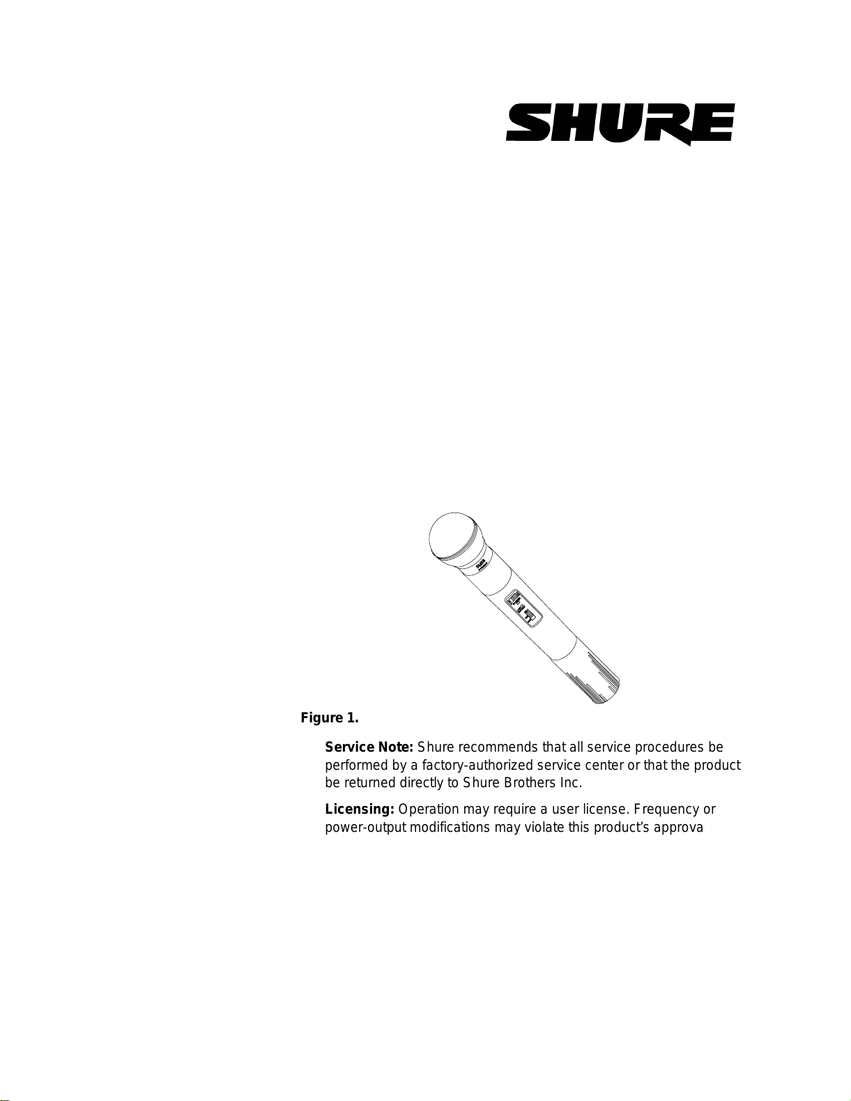
This section tells how to service and align the Shure Vocal Artist T2
Microphone-Transmitter (Figure 1). The single-channel, crystal-controlled transmitter operates in the 169 MHz to 216 MHz (FCC-approved
models) or 173–240 MHz (ETSI-approved models) VHF band. (The differences between the two versions of this product are explained on the next
page.)
E1999, Shure, Inc.
Printed in U.S.A.
Figure 1.
Service Note: Shure recommends that all service procedures be
performed by a factory-authorized service center or that the product
be returned directly to Shure Brothers Inc.
Licensing: Operation may require a user license. Frequency or
power-output modifications may violate this product’s approvals.
Contact your country’s communications authorities.
25C1018 (CC)
1
Characteristics
Page 3

Shure T2 Vocal Artist Microphone Transmitter
Circuit Description
This unit contains two interconnected circuit boards that comprise
the audio and RF sections, respectively. It is intended for use with the
matching T3 and T4 receivers.
FCC-Approved vs. ETSI-Approved Models: Models approved by
the Federal Communications Commission (assembly number 90–8690,
with boards marked 34A8494) have different sections from those approved by the European Telecommunications Standards Institute (assembly number 90–8705, with boards marked 34A8538). The FCC-approved version, sold in North America and many other places, uses only
the frequencies listed in Table 3 on page 12. The ETSI-approved version,
sold in Europe and many other places, uses only the frequencies listed
in Table 4 on page 13. Hence, the following circuit descriptions have separate sections for the two RF boards. The audio sections are the same
for all T2 models.
Audio Section
Input: The microphone element converts the sound source into an
electrical signal, which then enters the audio board through the center
contact of the head board (Figure 5, page 16).
Preamplifier Stage: This is centered in one section of operational
amplifier U102C. Externally accessible potentiometer R175 adjusts the
voltage gain of this stage over a 25 dB range.
Passive Pre-emphasis Network and Compandor: The network
(R145, C110, C111, C112, and R115) has a pole at 63 microseconds and
a zero at 12 microseconds. The NE571D integrated circuit compander
(U101A) provides 2:1 logarithmic compression of the audio signal.
Noise, Distortion, and Limiting: U102A lowers the noise floor, and
internal potentiometer R130 nulls the system audio distortion. Operational amplifier U102B, operating as a two-pole, active low-pass filter,
restricts the bandwidth of the system to the audio frequencies. PNP transistors Q103 and Q104 limit the level of the audio signal leaving the
audio section via U102B.
5 Vdc Bias and LED Drive Circuits: The NE571D’s identical second
channel (U101B) supplies regulated, low-noise 5 Vdc bias to various
audio and RF circuit points. Transistor Q105 provides “reverse battery
protection” to the circuit. Q106 drives LED D101 (“Power 0n”), and Q107
drives LED D102 (“Low Battery”).
RF Section: FCC-Approved Models
Audio Input: Processed audio enters R217, an internal potentiom-
eter that is adjusted for 15 kHz deviation (100% modulation) when the
audio section provides a –2.2 dBV, 1 kHz tone.
Characteristics
Oscillation: The audio then goes to varactor diode D201, which is
part of the modulated oscillator-tripler stage (Q201). The latter’s baseemitter circuit operates as a crystal-controlled Colpitts oscillator in the
2
25C1018 (CC)
Page 4

Shure T2 Vocal Artist Microphone Transmitter
20 MHz region. Fundamental-mode crystal Y201 is tuned 10 kHz below
series resonance by the series combination of frequency-netting coil
L209, diode D201, capacitor C214, and capacitor divider C224 and
C230.
Frequency and Temperature Stability: To ensure frequency stability despite changes in the battery voltage, regulated 5 Vdc bias is applied to the varactor diode and to the base of Q201. C224, C230, and
C214 provide temperature compensation.
Tuned Circuits (FCC-Approved Models)
Stage 1: The collector circuit of Q201 is tuned to the third harmonic
of the oscillator frequency (approximately 60 MHz) by L205, C225, C234,
L202, C217, C237, and C233. (The latter components also form a capacitively tapped voltage divider for matching into the base of Q203.)
The output is double-tuned to provide high spectral purity. Regulated dc
bias is again employed to minimize changes in loading on the oscillator
stage and to stabilize the drive levels.
Stage 2: Q203 operates as a frequency tripler, with the collector circuit tuned to the output frequency (for example, 180 MHz). In this case,
L204, C216, C238, C236, L210, C235, and C222 perform tuning and
impedance-matching functions. As in the preceding stage, regulated dc
bias is applied to the base circuit to stabilize the drive level, and the
output is double-tuned to provide spectral purity.
Stage 3: Q204 operates as a tuned amplifier. Resistive loading on
the input provides stability. The output circuit consists of a resonant tank
circuit (L203 and C213) capacitively coupled to a low-pass filter (C219,
L206, and C218). C213 and C219 provide a capacitively tapped voltage
divider for matching into the low-pass filter.
Final Output (FCC-Approved Models)
Transmitter: This can deliver up to +17 dBm (50 milliwatts) to the
antenna. No user adjustments permit this value to be exceeded. Testpoint I110 provides a termination point for the 50 Ω output. C211 and
L207 act as a series resonating network for the battery, which acts as the
antenna. The unit should be powered exclusively by a 9 Vdc dry battery
(an alkaline type like the Duracell MN1604 is recommended).
Voltage Measurements: With 9 Vdc applied to the unit, the following voltages should appear at the terminals of the output transistor:
S Vc = 8.88 Vdc
S Vb = .450 Vdc
S Ve = .473 Vdc
S Base current = 0.29 mAdc
S Emitter current = 21.5 mAdc
S Collector current = 21.8 mAdc
S Power input = 183 mW
25C1018 (CC)
3
Characteristics
Page 5

Shure T2 Vocal Artist Microphone Transmitter
The output power is +16.5 dBm (44.7 mW) into a 50 Ω load, at a frequency of 169.4445 MHz. At the lowest acceptable battery voltage of
6 Vdc, the final collector current drops to 15 mAdc and the output power
to +13.9 dBm (24.4 mW).
Spurious Emissions: To minimize the production and radiation of
spurious emissions and harmonic energy, and to promote stable operation, the collector of each RF stage is separately decoupled from the 9 V
supply by ferrite chokes, resistors, and bypass capacitors. The base circuits are similarly decoupled except they use resistor-capacitor (R-C)
networks, whose higher-impedance levels are more appropriate.
RF Section: ETSI-Approved Models
Audio Input: Processed audio enters R201, an internal potentiom-
eter that is adjusted for 15 kHz deviation (100% modulation) when the
audio section provides a –2.2 dBV, 1 kHz tone.
Oscillation: The audio then goes to varactor diode D201, which is
part of the modulated oscillator-tripler stage (Q201). The latter’s baseemitter circuit operates as a crystal-controlled Colpitts oscillator in the
20 MHz region. Fundamental-mode crystal Y201 is tuned 10 kHz below
series resonance by the series combination of frequency-netting coil
L201, diode D201, capacitor C203, and capacitor divider C206 and
C207.
Frequency and Temperature Stability: To ensure frequency stability despite changes in the battery voltage, regulated 5 Vdc bias is applied to the varactor diode and to the base of Q201. C203, C206, and
C207 provide temperature compensation.
Tuned Circuits (ETSI-Approved Models)
Stage 1: The collector circuit of Q201 is tuned to the third harmonic
of the oscillator frequency (approximately 60 MHz) by L202, C208, C244,
C210, L203, C214, C213, and C215. (The latter components also form a
capacitively tapped voltage divider for matching into the base of Q202.)
The output is double-tuned to provide high spectral purity. Regulated dc
bias is again employed to minimize changes in loading on the oscillator
stage and to stabilize the drive levels.
Stage 2: Q202 operates as a buffer, with the collector circuit tuned to
the output frequency (for example, 60 MHz). In this case, L204, C216,
C245, C218, L205, C222, C221, and C224 perform tuning and impedance-matching functions. As in the preceding stage, regulated dc bias is
applied to the base circuit to stabilize the drive level, and the output is
double-tuned to provide spectral purity.
Stage 3: Q203 operates as a frequency tripler, with the collector circuit tuned to the output frequency (for example, 180 MHz). In this case,
L206, C226, C227, C229, L207, C230, and C232 perform tuning and
impedance-matching.
Characteristics
Stage 4: Q204 operates as a tuned amplifier. Resistive loading on
the input provides stability. The output circuit consists of a resonant tank
4
25C1018 (CC)
Page 6

Shure T2 Vocal Artist Microphone Transmitter
circuit (L203 and C213) capacitively coupled to a low-pass filter (C219,
L206, and C218). C213 and C219 provide a capacitively tapped voltage
divider for matching into the low-pass filter.
Final Output (ETSI-Approved Models)
Transmitter: This can deliver up to +11.5 dBm (14 milliwatts) to the
antenna. No user adjustments permit this value to be exceeded. Testpoint TP6 provides a termination point for the 50 Ω output. C243 and
L211 act as a series resonating network for the battery, which acts as the
antenna. The unit should be powered exclusively by a 9 Vdc dry battery
(an alkaline type like the Duracell MN1604 is recommended).
Voltage Measurements: With 9 Vdc applied to the unit, the fol-
lowing voltages should appear at the terminals of the output transistor:
S Vc = 8.83 Vdc
S Vb = .097 Vdc
S Ve = .32 Vdc
S Base current = 0.27 µAdc
S Emitter current =9.67 mAdc
S Collector current = 9.67 mAdc
S Power input = 87 mW
The output power is +9.5 dBm (8.9 mW) into a 50 Ω load, at a frequency of 169.4445 MHz. At the lowest acceptable battery voltage of
6 Vdc, the final collector current drops to 8.84 mAdc and the output
power to +7.3 dBm (5.4 mW).
Spurious Emissions: To minimize the production and radiation of
spurious emissions and harmonic energy, and to promote stable operation, the collector of each RF stage is separately decoupled from the 9 V
supply by ferrite chokes, resistors, and bypass capacitors. The base circuits are similarly decoupled except they use resistor-capacitor (R-C)
networks, whose higher-impedance levels are more appropriate.
25C1018 (CC)
5
Characteristics
Page 7

Shure T2 Vocal Artist Microphone Transmitter
Notes
Notes
6
25C1018 (CC)
Page 8

Preliminary Tests
Listening Tests
Before disassembling the unit, operate it to determine whether it is
functioning normally.
Focused Testing: First and most important: Review any customer
complaint or request and focus your tests on any reported problem for
both listening and functional tests. For example, many complaints are for
“short range” and “drop-outs.” In such cases, perform only the RF tests in
this section to verify the problem. If the unit passes these, there is a
strong indication that the customer is using the product incorrectly (e.g.,
not keeping the transmitter in the receiver’s line of sight, not avoiding
metal enclosures or TV interference). Return the unit to the customer
together with an explanation of the proper set-up procedures.
Functional Test
For complaints of distortion or other audio problems, try a “standard”
microphone cartridge (you should have one of each cartridge on-hand
for testing) and perform the audio tests in this section.
Shure T2 Vocal Artist Microphone Transmitter
RF Tests
Note: Most of the following tests can be performed without disassembling the unit.
1. Install a fresh 9 V battery in the T2, mute its audio, and turn it on.
2. Measure current drain: it should not exceed 35 mA.
3. Maximize the signal received on the spectrum analyzer by attaching a telescoping whip antenna to it. Then measure the
near-field output power: it should be 7 dBm (FCC-approved
model) or 3 dBm (ETSI-approved model).
(If you are unsure of the results you obtained here, measure the
output power conductively by soldering a 50 Ω cable to the output of the transmitter. Verify that the output power is 15 dBm,
2 dBm [FCC-approved model] or 10 dBm, 2 dBm [ETSI-ap-
proved model].)
4. Verify that the carrier frequency of the transmitter varies from its
nominal value by no more than "6 kHz.
5. Check for an intermittent problem by shaking the transmitter and
tapping on it. As you do so, try to keep it at a constant distance
from the spectrum analyzer. Verify that the output power on the
spectrum analyzer shows no large and sudden drops in power
level (it will, however, vary a few dB with hand position).
25C1018 (CC)
6. Turn off the T2.
If the transmitter passes the above tests, its RF circuits are
working as designed.
7
Preliminary Tests
Page 9

Shure T2 Vocal Artist Microphone Transmitter
Audio Tests
A: Verify the Matching Receiver
1. Make sure that the receiver is turned off. Connect the signal
generator to the receiver through a 50 Ω cable. Tack-solder the
center conductor to the antenna input and ground the shield of
the cable to pcb ground. Turn on the receiver.
2. Set the RF signal generator as follows:
Amplitude: –50 dBm
Modulation: 1 kHz
Deviation: 15 kHz
Frequency: T2 operating frequency
3. Connect the audio from the unbalanced output to the audio analyzer with a 3.3 kΩ load. Turn the Volume control all the way up.
4. Engage the 400 Hz and 30 kHz filters on the audio analyzer.
Verify the following:
S For the T3 and T4 the audio level is 400 mVrms ("90 mV)
S For the T4N the audio level is 626 mVrms ("120 mV)
S thd = <0.75%
B: Check the Transmitter
Units That Pass
good, then the system is functioning as expected and shouldn’t require
tuning and alignment. Inform the customer that the product has retested
within specifications.
1. Disconnect the signal generator from the receiver. Monitor the
receiver’s unbalanced audio output with a 3.3 kΩ load and the
audio analyzer. Make sure the receiver’s Volume control is at its
maximum setting.
2. Replace the microphone cartridge on the T2 with the test head.
Set the unit’s Gain control to minimum and unmute the audio.
3. Inject a 775 mV, 1 kHz signal from the audio analyzer into the
adapter cable and verify the following:
S the amplitude from receiver’s unbalanced output equals
400 mVrms ("90 mV)
S thd = <0.75%
4. Change the frequency of the audio generator to 100 Hz and disengage the 400 Hz high-pass filter from the audio analyzer.
Verify that the audio level is –1.0 dB ("0.7 dB) relative to the
level measured in step 3.
5. Change the frequency of the audio generator to 10 kHz and reengage the 400 Hz high-pass filter. Verify that the audio level,
relative to that measured in step 3, is –3.5 dB, "2 dB.
If the system components pass these tests and the microphone is
Preliminary Tests
8
25C1018 (CC)
Page 10
Shure T2 Vocal Artist Microphone Transmitter
Disassembly and Assembly
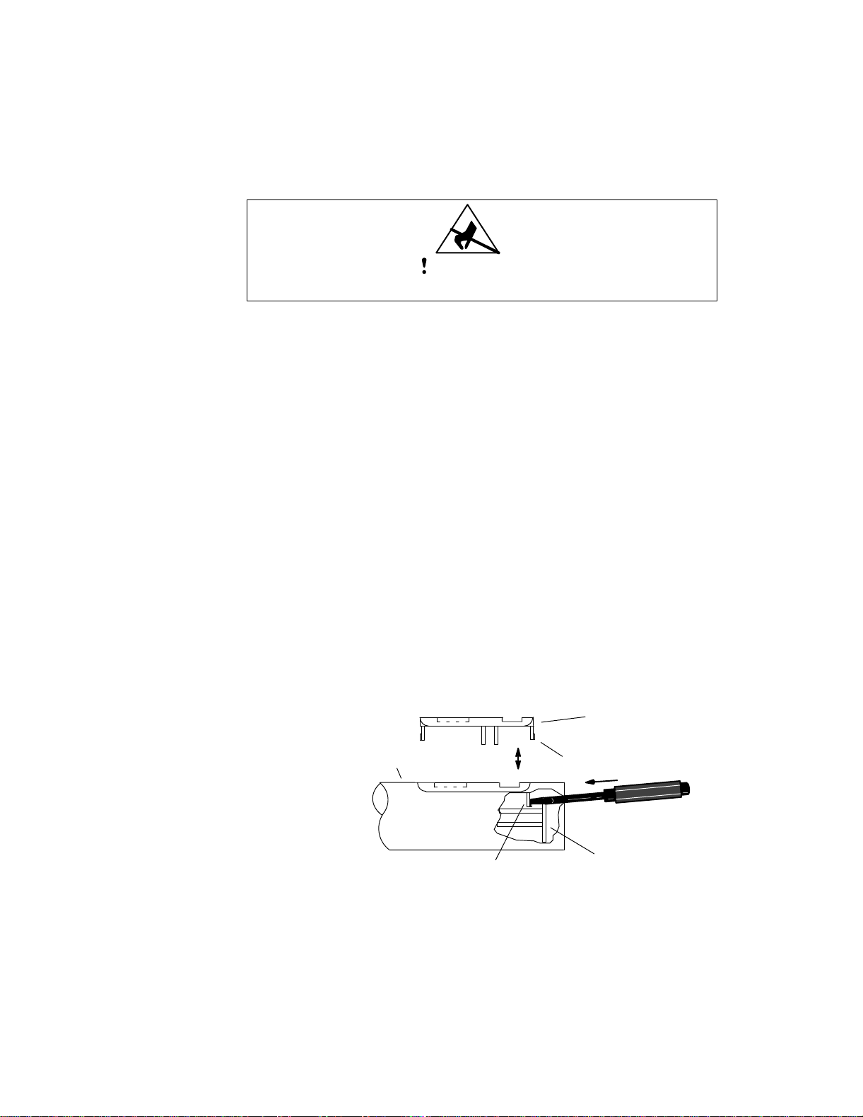
To access the printed circuit (pc) boards, disassemble the transmitter
(refer to Figures 2 and 3 on pages 9 and 10).
CAUTION
Observe precautions when handling this static-sensitive device.
Disassembly
1. Turn off the Power switch.
2. Unscrew the transmitter battery cup and remove the battery.
3. Unscrew the microphone cartridge.
4. If necessary, remove the microphone-transmitter subassembly:
(a) Use snap ring pliers to remove the retaining ring from in-
side the microphone handle.
(b) Remove the bezel by carefully inserting a small screwdriver
into the microphone handle, pressing the blade against the
plastic bezel tab, and prying it up (Figure 2). Remove the
label plate and switch actuators (Figure 3, page 10).
Note: Newer bezels have the labeling printed directly on
their faces; there are no separate label plates.
(c) As you slide out the transmitter subassembly (audio, RF,
and head circuit boards) from the handle, note how it was
positioned in the internal guides.
bezel
handle
tab
(Right-side view)
tab
circuit-board
subassembly
25C1018 (CC)
Figure 2. Removing the Bezel
9
Disassembly and Assembly
Page 11
Shure T2 Vocal Artist Microphone Transmitter
ÁÁÁ
Reassembly
1. Insert the transmitter subassembly (audio, RF, and head circuit
boards) into the internal guides of the handle (Figure 3).
2. Orient the retaining ring so its gap will fit over the flat edge of the
head board (to avoid shorting the board). Use snap-ring pliers to
insert the retaining ring into the groove inside the handle.
3. Drop in the switch actuators and position the label plate (older
bezels only) over them. Position the bezel over the switches
then press until it snaps into place.
4. Screw on the microphone cartridge and ball screen. Install a battery (if desired) and screw on the battery cup.
ball screen
retaining
A
ball screen
microphone
cartridge
BG 3.1
ring
RF
circuitboard
head
board
Figure 3.
switches
circuitboard
guides
microphone
cartridge
SM 58
audio
circuitboard
(older, BG 3.0
A
gain
control
handle
cartridge)
(older bezels only)
label plate
access
to gain
control
A
9 V alkaline
battery
bezel
battery
cup
switch
actuators
Disassembly and Assembly
10
25C1018 (CC)
Page 12

Shure T2 Vocal Artist Microphone Transmitter
Service Procedures
Reference Material
The Shure Wireless System T Series User’s Guide describes the
product, tells how to operate it, and provides troubleshooting and technical data.
Special Equipment and Tools
In addition to the standard items described in the Wireless Service
Equipment manual, you will need:
S to verify that the system is working properly, obtain the receiver
with which the transmitter is used (usually a T3 or T4); otherwise, use the modified SC4 receiver described in the equipment
manual
S a small flat-blade screwdriver to remove the bezel
S snap-ring pliers to remove and re-insert the retaining ring
S hand-made high-impedance probe (see the Service Equipment
manual)
System Operating Frequencies
Each transmitter circuit board is marked with a group letter that identifies the range of frequencies on which the transmitter can operate. Note
that Table 1 applies only to T2 transmitters that are FCC-approved, and
Table 2 applies only to T2 transmitters that are ETSI-approved.
Frequency Coverage: Earlier models used the same family of RF
boards (with Groups A, B, and C) for all the frequencies offered worldwide at that time. Now there are separate board assemblies for units approved by the ETSI. If you have a frequency from Table 4, you have an
ETSI-approved model; if you have a frequency from Table 3, you have an
FCC-approved model.
Pc Board Groups for
FCC-Approved Models
Group Frequency Range
A 169.000–183.975 MHz
B 184.000–198.975 MHz
C 199.000–215.975 MHz
Used with pcb assembly 90_8690
(pcb marking 34A8494).
Table 1
25C1018 (CC)
11
Service Procedures
Page 13
Shure T2 Vocal Artist Microphone Transmitter
Pc Board Groups for
ETSI-Approved Models
Group Frequency Range
A 169.000–173.975 MHz
B 174.000–180.975 MHz
C 181.000–187.975 MHz
D 188.000–194.975 MHz
E 195.000–201.975 MHz
F 202.000–208.975 MHz
G 209.000–215.975 MHz
H 216.000–222.975 MHz
K 216.000–239.975
Used with pcb assembly 90_8705
Tables 3 and 4 provide information for identifying the system frequency. The Crystal Letter Code, when used with the appropriate Shure
model number, identifies a specific operating frequency for both transmitters and receivers. Note that, although a Crystal Letter Code always designates a specific frequency, it may be used with different Group Letters
on other products.
Table 2
(pcb marking 34A8538).
Table 3
T2 System Operating Frequencies for
FCC-Approved Models
Crystal
Group
Used with pcb assembly 90_8690
Code
A V 169.445
A W 171.845
A CA 176.200
A CC 177.600
A CE 182.200
A CF 183.600
B CG 186.200
B CL 192.200
C CQ 202.200
C CV 208.200
(pcb marking 34A8494).
Operating
Freq. (MHz)
Service Procedures
12
25C1018 (CC)
Page 14

Shure T2 Vocal Artist Microphone Transmitter
Table 4
T2 System Operating Frequencies for
ETSI-Approved Models
Crystal
Group
Code
A AQ 173.800
B ZZ 174.500
B BB 175.000
B NB 175.000
B ND 176.600
B NE 177.600
C NH 182.000
C NK 183.600
C NL 184.600
C S 184.000
D NP 189.000
D NR 190.600
E NX 197.600
E NY 198.600
E NZ 200.350
Operating
Freq. (
MHz)
Changing the Frequency
The operating frequency of the T2 transmitter may be changed within a specific Group by changing the crystal on the pc board. (For Group
information, see the preceding subsection). Check the transmitter for
proper operation before changing its operating frequency. After installing
the new crystal, perform the alignment procedures. Then run an operational test to ensure that the transmitter is functioning properly. Finally,
update the label to show the new frequency and letter identification code.
E PU 201.650
F PB 203.000
F PD 204.600
H PP 217.000
H PR 218.600
H PS 219.600
K PV 232.825
K PX 233.125
K PY 234.625
K PZ 237.325
Used with pcb assembly 90_8705
(pcb marking 34A8538).
25C1018 (CC)
13
Service Procedures
Page 15

Shure T2 Vocal Artist Microphone Transmitter
Note: To ensure proper operation, obtain the crystal from Shure and
verify that it operates within the frequency range of the pc board.
Since crystals are marked with the nominal oscillating frequency, not
with a letter code, you can use the following equation to determine
the frequency at which a transmitter will operate with a given crystal:
Carrier Frequency = (9 x nominal crystal freq. in MHz) – .09
FCC- and ETSI-Approved Models
To accommodate the different frequencies and requirements, Shure
supplies the T2 with different RF boards for FCC-approved models (used
in North America and other places) and ETSI-approved models (used in
Europe and other places). Although the RF alignment procedures are
similar for the two boards, there are some differences, especially in the
number of tuning stages and in the numbering of components and test
points. The audio-alignment procedures are the same for both versions
of the T2.
Note: Before the introduction of a distinct RF board for ETSI 300 922
requirements, all units shared the same RF and audio boards.
Alignment
Test Conditions
Drawings for Different Versions
At the back of this manual are diagrams of the circuit boards and
schematics for the original versions of the audio and RF boards as well
as for the current versions of the audio board, FCC-approved RF board,
and ETSI-approved RF board. Refer to the circuit-board diagrams for the
test points.
The RF and audio alignments are generally done together, as a
single, continuous procedure. Before beginning, do the setup described
in the following subsection, “Test Conditions.” Unless specified for FCC-
or ETSI-approved models, the alignment procedures apply to all models.
The following test conditions apply to all versions unless otherwise
specified:
S An external 9-volt supply is connected to the battery terminals
(J101 and J102).
S The Gain pot (R125) is set to its mid-range position.
S The audio analyzer’s 400 Hz high-pass and 30 kHz low-pass
filters are pressed in.
Service Procedures
FCC-Approved Units
1. Obtain a 50 Ω test cable for connecting the circuit boards to various test equipment. (To construct this cable, see “50 Ω Test
Cable Assembly” in the Wireless Service Equipment manual.)
14
25C1018 (CC)
Page 16

Shure T2 Vocal Artist Microphone Transmitter
2. Tack-solder the ca ble to side 1 of the RF circuit board as follows:
S Center conductor to the 50 Ω solder pad, I210
S Shielding to I2GN (on older versions, IGND)
ETSI-Approved Units
1. Obtain a 50 Ω coaxial test cable for connecting the circuit boards
to various test equipment. (To construct this cable, see “50 Ω
Test Cable Assembly” in the Wireless Service Equipment manual.)
2. Tack-solder the ca ble t o the bottom of the RF circuit board as follows:
S Center conductor to the 50 Ω solder pad, TP6
S Shielding to TP7 (ground)
High-Impedance Probe for TP5: When measuring test point 5,
fashion a high-impedance probe on the end of the test cable by connecting a 50 Ω resistor between the center conductor and the shield, and a
0.5 pF capacitor to the end of the center conductor (see the following
illustration).
Display Checks
shield
0.5 pF
50 Ω
Figure 4. High-Impedance Probe for ETSI-Approved Models
All Units
3. Carefully remove C240 (domestic units) or C242 (ETSI units) from
the RF board.
Note: This disconnects the battery antenna to allow accurate
conductive-power measurements.
1. Connect the 9 Vdc power supply to the audio board: the positive
lead to I140 (the positive battery terminal), and the negative lead
to I145 (ground).
2. Slide S101 (Power) to “On” (toward the board number), and
S102 (Mic) to “Off” (away from S101): the green LED should
glow. If it doesn’t, there is a circuit malfunction.
25C1018 (CC)
3. Reduce the power-supply voltage to 6 Vdc: the red LED should
glow.
4. Return the power supply voltage to 9 Vdc.
15
Service Procedures
Page 17

Shure T2 Vocal Artist Microphone Transmitter
Audio Board (top)
Power
(green)
D103
Power
On/Off
S101
Low battery
(red)
D101
Mic
R130
On/Off
S102
Head Board (front view)
Audio Out
RF
(to
board)
+5 V
Audio In
(from audio board)
+9 V
Gnd Gnd
C107
+
(to cartridge)
U101
+9 V
R125
J102
–
+
J101
U102
Gnd
+9 V
Audio In
(to audio board)
+9 V
Gold-plated contacts
FCC-Approved Model RF Board (top)
Audio In
(from cartridge)
I210
IGnd
J101
+
–
J102
L209
ETSI-Approved Model RF Board (top)
L201 R201 C214 C222 C226
R217
Y201
TP5 (base of
Q202)
Y201
C217
C216
C216
TP6
TP7
J101
+
–
J102
Figure 5. Major Components Referred to in the Alignment Procedures
Service Procedures
16
25C1018 (CC)
Page 18

Shure T2 Vocal Artist Microphone Transmitter
RF Alignment: FCC-Approved Models
Do not apply modulation during the following RF alignment proce-
dures.
Note: If you cannot achieve any of the settings described in these
procedures, see “Bench Checks,” starting on page 23.
1. Make sure that the Mic switch (S102) is turned to ”Off.”
2. On the spectrum analyzer, set the center frequency to the frequency of the T2. Then make the following settings:
S Span: 1 MHz
S Reference level: +20 dBm
S Scale: 10 dB/div.
3. Connect the 50 Ω output cable to the spectrum analyzer.
A: Output Power (FCC-Approved Models)
1. With a yellow Toray non-conductive tuning tool, adjust C217 and
C216 for maximum (peak) output power on the spectrum analyzer. If the signal is very near the top of the screen, switch the
scale to 2 dB/div.
2. The output power should be 15 dBm, ±2 dBm (compensate for
cable losses in this calculation).
B: Frequency Adjustment (FCC-Approved Models))
1. Connect the 50 Ω output cable to the frequency counter through
the 20 dB attenuator. With a pink Toray driver, adjust L209 to set
the RF carrier frequency to the operating frequency
(±1 kHz—see Table 3 on page 12).
2. Reconnect the 50 Ω output cable to the spectrum analyzer. Con-
firm that the output power remains within specification. If not,
readjust C217 and C216 as described in the preceding “Output
Power” subsection.
C: Spurious Emissions (FCC-Approved Models)
1. Set the spectrum analyzer as follows:
S Scale: 10 dB/div
S Start Frequency: 10 MHz
S Stop Frequency:1 GHz
S Reference level: 20 dBm
2. Check the level of spurious emissions: All must be at least
30 dB below the carrier level. If necessary, retune C217 and
C216.
25C1018 (CC)
17
Service Procedures
Page 19

Shure T2 Vocal Artist Microphone Transmitter
D: Current Drain (FCC-Approved Models)
1. With a digital multimeter, measure the current drain of the transmitter: it should be less than 35 mA. If it is too high, try detuning
C216, but make sure that the power and spurious response remain within specification.
2. Check for 9 Vdc (±0.35 Vdc) at +9 V on the head board (I133 on
the audio board).
RF Alignment: ETSI-Approved Models
Do not apply modulation during the RF alignment procedures.
Note: If you cannot achieve any of the settings described in these
procedures, see “Bench Checks,” starting on page 23.
1. Slide the Mic switch (S102) to the ”Off” position.
2. On the spectrum analyzer, set the center frequency to one-third
the frequency of the T2. Then make the following settings:
S Span: 30 MHz
S Reference level: +20 dBm
S Scale: 10 dB/div.
3. Connect the high-impedance probe to the spectrum analyzer.
A: Output Power (ETSI-Approved Models)
1. Connect the high-impedance probe to TP5 (the base of Q202).
2. With a yellow Toray non-conductive screwdriver, adjust C214 for
maximum (peak) output power on the spectrum analyzer. For
better resolution while tuning, switch the scale to 2 dB/div and
adjust the reference level to the center of the screen.
3. Remove the high-impedance probe. Connect the standard 50 Ω
output cable to TP6 (before antenna-matching).
4. Plug the BNC end of the 50 Ω cable into the spectrum analyzer.
5. Set the center frequency to the frequency of the T2.
6. Adjust C216 and C222 for maximum (peak) output power on the
spectrum analyzer.
Note: C216 is not tuneable on earlier ETSI-approved units.
B: Frequency and Final Output Power (ETSI-Approved
Models)
1. Connect the 50 Ω output cable to the frequency counter. With a
pink Toray driver, adjust L201 to set the RF carrier frequency to
within ±1 kHz of the operating frequency (see Table 4, page 13).
2. Reconnect the 50 Ω output cable to the spectrum analyzer. Peak
C226 for maximum output power on the spectrum analyzer.
Service Procedures
3. Confirm that the output power is 9.5 dBm (±2 dBm).
18
25C1018 (CC)
Page 20

Shure T2 Vocal Artist Microphone Transmitter
C: Spurious Emissions (ETSI-Approved Models)
1. Set the spectrum analyzer as follows:
S Scale: 10 dB/div
S Start Frequency: 10 MHz
S Stop Frequency:1 GHz
S Reference level: 20 dBm
2. Check the level of spurious emissions: All must be at least
44 dB below the carrier level. If necessary, retune C226.
D: Current Drain (ETSI-Approved Models)
1. With a digital multimeter, measure the current drain of the transmitter: it should be less than 35 mA. If it is too high, try detuning
C226, but make sure that the power and spurious response remain within specification.
2. Check that 9 Vdc (±0.35 Vdc) is present at the head board +9 V
location (I133 on the audio board).
Audio Alignment (Both Models)
The audio boards on the FCC-approved and ETSI-approved models
are identical except for the pcb number printed on the board. (These
numbers differ because the boards are made as parts of larger assemblies for the two different models.)
The audio board has changed relatively little in the history of the T2.
Two examples of changes are the renumbering of the LEDs (the green
used to be D101, and the red, D102) and some slightly different designations (e.g., I1GN used to be IGND).
E: Setup
1. Disconnect the power supply from the T2.
2. Unsolder the test cable.
3. Replace C240 (domestic units) or C242 (ETSI units) on the RF
board.
4. Slide the board assembly, battery terminals first, into the test
handle: be sure to align the sides of the assembly with the handle’s inner tracks. Alternatively, slide the assembly through the
test ring.
5. Screw the audio test head into the handle or ring. Connect a
BNC-to-BNC cable between the audio analyzer and the test
head.
25C1018 (CC)
6. Reconnect the 9 V power supply to the battery terminals of the
T2.
7. Place the Mic switch in the “On” position. Verify that the green
power LED (D103) lights steadily.
19
Service Procedures
Page 21

Shure T2 Vocal Artist Microphone Transmitter
F: Modulation Calibration
1. Set the output of the audio analyzer as follows:
S Frequency: 1 kHz
S Amplitude: 230 mV
S Measurement: Ac Level
S Filters: 400 Hz and 30 kHz on
2. Adjust the Gain (R125) so the output at the positive side of C107
is 0 dBu, ±0.1 dB (775 mV, ±50 mV). See Figure 5, page 16.
Note: At this point you may want to press the Log/Lin button on
the audio analyzer (to measure in dBm) and then press the Ratio
button to perform the relative measurement for frequency response.
G: Frequency Response
1. Set the audio analyzer as follows:
S Frequency: 100 Hz
S 400 Hz High-Pass filter: Disengaged
2. Verify that the audio level at the positive side of C107 is
–0.5 dB, ±0.5 dB, relative to the level you set in Step 2 of sub-
section F.
3. Reset the audio analyzer as follows:
S 400 Hz High-Pass filter: Engaged
S Frequency: 10 kHz
4. Check that the audio level at the positive side of C107 is equal to
3 dB, ±0.5 dB, relative to the level you set in Step 2 of subsection F.
H: Deviation Reference Voltage
1. Turn off the T2 Power switch.
2. Obtain a receiver set to the same frequency as the T2 (this will
probably be the T3 or T4 that came with the T2).
Note: Alternatively, use a modified SC4 receiver for any transmit-
ter. Instructions for modifying and using an SC4 are in the Wire-
less Service Equipment manual.
3. Attach an antenna or an unshielded cable to the RF signal gen-
erator. Set the RF signal generator as follows;
S Frequency: Carrier
S Modulation: FM
S Modulation source: Int 1 kHz
S FM Deviation: ±15 kHz
S Amplitude: –38 dBm
Service Procedures
20
25C1018 (CC)
Page 22

Shure T2 Vocal Artist Microphone Transmitter
4. Make sure that the receiver’s yellow RF LED lights.
5. Set the receiver’s Volume control to the maximum position (full
clockwise rotation) and apply power to the receiver. On the T4,
set the Squelch control to its midpoint.
6. Measure the rms voltage developed across the unbalanced output of the receiver. The reading should be approximately 0 dBu
(775 mV), which corresponds to a deviation level of 15 kHz.
Record this voltage as the Deviation Reference Voltage.
Note: At this point you may want to press the Log/Lin button on
the audio analyzer (to measure in dBm) and then press the Ratio
button to perform the relative measurement in the next section.
7. Turn off the RF output from the signal generator.
I: Deviation Adjustment
1. Make sure that C240 is on the RF board, so that the antenna is
connected).
2. Remove the power-supply leads and attach a new 9 V battery.
3. Connect the output of the audio analyzer to the test head.
4. Set the frequency of the audio analyzer to 1 kHz. Make sure that
0 dBu (775 mV) is present at the positive side of C107.
5. Measure the rms voltage at the unbalanced output of the receiver. Adjust R217 to obtain voltage within ±1 dB of the deviation
reference voltage that you recorded earlier (see the end of the
preceding subsection).
J: Distortion Adjustment
1. Set the audio analyzer for “Distn” (total harmonic distortion).
2. Adjust R130 for minimum distortion out of the receiver (it should
measure less than 1%).
Note: This completes the alignment procedures. Refer to the “Reas-
sembly” instructions earlier in this manual.
25C1018 (CC)
21
Service Procedures
Page 23

Shure T2 Vocal Artist Microphone Transmitter
Notes
Notes
22
25C1018 (CC)
Page 24

Bench Checks
The tests for power and audio apply to all T2 units. Those involving
the RF board differ for FCC-approved and ETSI-approved units; hence
this section includes two separate sets of procedures for RF testing.
Dc Power
n Verify that 9 Vdc (±0.35 Vdc) is present at I+9.0 (on the bottom
of the audio board—see Figure 6, page 33). If this voltage is low,
check it at I133. Trace the circuitry back to the power supply to
see where the loss occurs. Check:
S power switch
S bias on Q105
S L101
S circuit-board ground for 0 V
n If you have a short to ground from 9 V, try isolating different parts
of the circuit. Narrow it down to the RF or audio section. Look for
foil shorts, solder bridges, and capacitors that have been
installed backwards.
n Check for 5 Vdc (±0.25 Vdc) at I147. If the correct voltage is not
present, check I+5 (pin 7 of U101). Then check:
S pin 13 of U101 for 9 V
S values of R133, R135, and R137
Note: If you are measuring dc voltages at points where RF sig-
nals are present, use a 10 kΩ resistor at the probe to prevent
loading the circuit. To remove the RF signal, remove the crystal.
Shure T2 Vocal Artist Microphone Transmitter
Audio
25C1018 (CC)
All the steps in this section comprise a methodical way of determining where the audio signal is being interrupted:
n Check for audio at pin 7 of U102. If it is not present, check that
the dc bias at pins 5, 6, and 7 of U102 is `4.5 Vdc (half the level of the supply voltage). If the correct voltage is not present:
S Trace the circuitry: this bias derives from the 9 V line through
voltage divider R103 and R105, then through R106 to pin 5.
S Look for open vias (through-hole connections between board
layers), foil shorts, incorrect parts, and bad connections.
n If there is audio at pin 7 of U102 but not at pin 14, check the dc
bias at pins 12 and 13 (`1.8 Vdc) and pin 1 (`3.7 Vdc). If the
correct voltage is not present:
S Trace the circuitry: this dc bias proceeds from pin 9 of U101
through R107 to pin 12 of U102.
S Check (a) the parts in the feedback path from pin 14 to
pin 13, (b) the parts connected to pin 7, and (c) the connections from U102 to U101.
23
Bench Checks
Page 25

Shure T2 Vocal Artist Microphone Transmitter
n Check the connections from pin 14 of U102 to the next stage, to
the limiter (Q103), and to pin 15 of U101.
n Check the bias voltage (`4 Vdc) on pins 8, 9, and 10 of U102. If
the correct voltage is not present:
S Make sure the Mic switch is set to “On.”
S Trace the bias circuit from the 5 V line through R104 to
pin 10 of U102.
S Check the values in the feedback path from pin 8 to pin 9 of
U102, and the path to Q104 and pin 16 of U101.
Distortion
n Make sure the analyzer’s 400 Hz high-pass and 30 kHz low-
pass filters are pressed in.
n Pin 9 of U101 should read `1.8 Vdc.
n As you turn R130, the dc level on its wiper should change from
`1.5 V to 3.5 V. If it does not, check R129, C125, R130, R141,
R140, R126, and the parts tied to pin 9 of U101.
n Check the audio level.
n Lastly, replace D201 and Y201.
Frequency Problem: FCC-Approved Units
n Make sure the RF carrier is at least 10 dB higher than the spuri-
ous emissions, to allow the frequency counter to lock on.
n Check L209 for the proper group and make sure its core is not
cracked.
n Make sure the crystal (Y201) has the correct frequency.
n Check the dc bias for Q201 against the readings of a unit known
to be operating correctly.
n Make sure that D201 is the correct varactor and has 5 Vdc on its
cathode.
n Check the parts and values of the oscillator circuit (from I218 to
I230).
n Look for shorts and opens.
Low Output Power: FCC-Approved Units
For these checks, terminate the transmitter’s output with a 50 Ω load
between I210 and ground. If you have interconnected the audio and RF
boards for testing, temporarily remove C240 to disconnect the battery
antenna.
n Check the carrier output power after the oscillator stage (I230).
If there is no signal, refer to the preceding subsection, “Frequency Problem.”
The remaining steps perform basically similar diagnostics for each of
the three RF stages:
Bench Checks
24
25C1018 (CC)
Page 26

Shure T2 Vocal Artist Microphone Transmitter
n Make sure the Board Group is the correct one for the desired
frequency.
n Stage 1: Make sure that rotating C217 360 degrees in either di-
rection produces two separate peaks in the carrier output amplitude. If there is only one peak, check the color (value) of C217
and the values of L205, C225, C234, L202, and C233. Check
the bias on Q201. Lastly, replace Q201.
n Stage 2: Make sure that rotating C216 360 degrees in either di-
rection produces two separate peaks in the carrier output amplitude. If there is only one peak, check the color (value) of C216
and the values of L204, C238, L210, C235, C222, and C226.
Check the bias on Q203. Lastly, replace Q203.
n Stage 3: Check the dc bias on Q204 and the values of all the
parts from the base of Q204 to I210. Lastly, replace Q204.
n If the power is slightly low and the spurious level is high, check
for wrong or open coils at L202, L210, and L206.
n Check the emitter bypass capacitors (C226 and C223) and the
collector bypass capacitors (C207 and C208), which can also
affect the tuning and power gain of the RF stages. If RF level is
not the same on both sides of one of these capacitors, that part
is probably defective.
Excessive Current Drain: FCC-Approved Units
n Try readjusting C216 for lower current drain while maintaining
output power to specification. If the current drain is still excessive (the factory setting is 35 mA), check for the following:
S short
S wrong resistor value
S defective capacitor
S correct value of R219 for the frequency group
n As a last resort, try changing Q204.
Deviation: FCC-Approved Units
n If R217 on the RF board cannot be adjusted to obtain a "15 kHz
deviation, try to isolate the problem to the audio or RF section by
doing the following:
S If I218 on the RF board does not measure –2.2 dBV
(775 mV), refer to the “Audio” section, page 23.
S If I218 has the right level, check R217, C220, C227, R208,
R216, D201, R209, L209, and C214. Also make sure that
the cathode of D201 is being supplied with a 5 Vdc bias from
the 5 V Line through R216 and R208. The value of C214 is
critical to the deviation sensitivity.
n As a last resort, try replacing D201 and Y201.
n Make sure the carrier is good: you need that to get any devi-
ation.
25C1018 (CC)
25
Bench Checks
Page 27

Shure T2 Vocal Artist Microphone Transmitter
Frequency Problem: ETSI-Approved Units
n Make sure the RF carrier is at least 10 dB higher than the spuri-
ous emissions, to allow the frequency counter to lock on.
n Check L201 for the proper group and make sure its core is not
cracked.
n Make sure the crystal (Y201) has the correct frequency.
n Check the dc bias for Q201:
VC = 8.83 V
VB = 0.97 V
VE = 0.32 V
n Make sure that D201 is the correct varactor and has 5 Vdc on its
cathode.
n Check the parts and values of the oscillator circuit.
n Look for shorts and opens.
Low Output Power: ETSI-Approved Units
For these checks, terminate the transmitter’s output with a 50 Ω load
between TP6 and ground. If you have interconnected the audio and RF
boards for testing, temporarily remove C242 to disconnect the battery
antenna.
n Check the carrier output power after the oscillator stage (TP5). If
there is no signal, refer to the preceding subsection, “Frequency
Problem.”
The remaining steps perform basically similar diagnostics for each of
the four RF stages:
n Make sure the Board Group is the correct one for the desired
frequency.
n Stage 1: Make sure that rotating C214 360 degrees in either di-
rection produces two separate peaks in the carrier output amplitude. If there is only one peak, check the values of C214, L202,
C208, C244, C210, L203, C213, and C215. Check the bias on
Q201. Lastly, replace Q201.
n Stage 2: Make sure that rotating C222 360 degrees in either di-
rection produces two separate peaks in the carrier output amplitude. If there is only one peak, check the values of C222, L204,
C216, C245, C219, L205, C221, and C224, Check the bias on
Q202. Lastly, replace Q202.
n Stage 3: Make sure that rotating C226 360 degrees in either di-
rection produces two separate peaks in the carrier output amplitude. If there is only one peak, check the values of C226, L206,
C227, C229, L207, C230, and C232. Check the bias on Q203.
Lastly, replace Q203.
n Stage 4: Check the dc bias on Q204 and the values of all the
parts from the base of Q204 to TP6. Lastly, replace Q204.
Bench Checks
26
25C1018 (CC)
Page 28

Shure T2 Vocal Artist Microphone Transmitter
n If the power is slightly low and the spurious level is high, check
for wrong or open coils at L205, L207, and L210.
n Check the collector bypass capacitors for the RF stages (C220,
C227, and C234) and the collector bypass capacitor for Q203
(C228), which can also affect the tuning and power gain of the
RF stages:
S If RF level is not the same on both sides of one of these ca-
pacitors, that part is probably defective.
S The RF level between the collector of one transistor and the
base of the next should drop approximately 10 dB. Check
any stage that drops more than 12 dB.
Excessive Current Drain: ETSI-Approved Units
n Try readjusting C226 for lower current drain while maintaining
output power to specification. If the current drain is still excessive (the factory setting is 35 mA), check for the following:
S short
S wrong resistor value
S defective capacitor
S value of R218 (that it is correct for the frequency group)
n As a last resort, try changing Q204.
Deviation: ETSI-Approved Units
n If R201 cannot be adjusted to obtain a "15 kHz deviation, try to
isolate the problem to the audio or RF section by doing the following:
S If TP1 on the RF board (or I109 on the audio board) does not
measure –2.2 dBV (775 mV), refer to the “Audio” section,
page 23.
S If the preceding level is correct, check R201, C201, C202,
R202, R203, D201, L201, and C203. Also make sure that
the cathode of D201 is being supplied with a 5 Vdc bias from
the 5 V line through R202 and R203.
n As a last resort, try replacing D201 and Y201.
n Make sure the carrier is good: you need that to get any devi-
ation.
25C1018 (CC)
27
Bench Checks
Page 29

Shure T2 Vocal Artist Microphone Transmitter
Distortion: ETSI-Approved Units
n Make sure the analyzer’s 400 Hz high-pass and 30 kHz low-
pass filters are pressed in.
n Pin 9 of U101 should read about 1.8 Vdc.
n As you turn R139, the dc level on its wiper should change from
about 1.5 V to 3.5 V. If it does not, check R139, C1, R141, R140,
R114, and the parts tied to pin 9 of U101.
n Check the audio level.
n Lastly, replace D201 and Y201.
Bench Checks
28
25C1018 (CC)
Page 30

Shure T2 Vocal Artist Microphone Transmitter
Replacement Parts and Drawings
On the next page, the parts are listed according to the reference
designations from the pc boards and schematics. Parts shown on the
circuit diagram and not listed below are available at most electronic parts
distributors.
On the pages following the parts lists are the drawings of the printed
circuit boards and the schematics.
Product Changes
This section briefly describes significant changes as of this writing to
the T2.
RF Boards: The original RF board supported both North American
and a limited number of European frequencies. There are now two RF
boards. A slightly revised version of the original board, with a new layout,
supports only the frequencies for FCC-approved units, and a new board
supports a greatly expanded list of frequencies for ETSI-approved units.
RF Tuning on ETSI-Approved Units: C216 has been changed to a
variable capacitor, adding a stage in the tuning. Associated capacitor
C245 has also been changed. See the schematic for the frequency-dependent values of this capacitor.
Combined RF and Audio Board Numbers: Because the factory
now assembles the two boards as a single panel before separating
them, there is now a single part number for each combination: 90_8690
for the RF and audio boards on FCC-approved units, and 90_8705 for the
RF and audio boards on ETSI-approved units. When ordering, use the
appropriate assembly number but specify whether you want just the RF
board, just the audio board, or both. Note further that the audio boards
from the two assemblies are identical except for the part number printed
on the bottom.
Quad Op Amp: The earlier part (manufactured by Raytheon) was
replaced; the former value of associated resistor R107 was 100 kΩ.
LEDs and Layout: The LEDs were rearranged and renumbered, and
transistor Q108 and associated circuits were added. In addition, the audio layout was changed. These changes do not greatly affect the audio
alignment.
BG 3.1 Microphone: The earlier T230 models were supplied with
BG 3.0 microphone cartridges. The newer T231 models are supplied with
BG 3.1 cartridges. The earlier models will accept the new cartridges.
ID Resistors: To help assemblers identify the RF board used on
ETSI-approved units, the factory has added resistors R259 and R261.
They are not functional.
25C1018 (CC)
Frequency Changes: The “C” and “D” revisions to the ETSI RF
boards primarily consist of minor corrections to the drawings, adding the
“S” frequency and “K” group, and redesignating the “J” frequency “BB.”
29
Replacement Parts and Drawings
Page 31

Shure T2 Vocal Artist Microphone Transmitter
Parts Designations
The following comments apply to the parts list and the schematic:
Resistors: All are surface-mount, 1/10 W rating, and 1% tolerance.
Capacitors: Unless otherwise noted, non-polarized capacitors are
surface-mount NPO dielectric types with a 100 V capacity and 5% tolerance; polarized capacitors are tantalum types.
Temperature-Compensating Capacitors (N750 designation):
FCC-Approved RF Boards: C214, C224, C230.
ETSI-Approved RF Boards: C203, C206, C207.
Replacement Parts and Drawings
30
25C1018 (CC)
Page 32

Shure T2 Vocal Artist Microphone Transmitter
Table 1
T2 Replacement Parts
Reference
Designation Description Shure Part No.
A1 FCC-approved RF/Audio pro-
grammed circuit board assembly
A2 ETSI-approved RF/Audio pro-
grammed circuit board assembly
A3 Head pcb assembly 34A1090D
MP1 Gold-plated spring contacts 53F2039A
MP2 Actuators *old type* 65A8225
MP3 Actuator *current oval type* 65C8298
MP4 Battery cup 65A8206A
MP5 Bezel * for older version handle * 65B8207A no longer available
MP6 Bezel *current oval type* 65B8299
MP7 Handle *** Old version *** 65A8220A not available
MP8 Handle * Current type.* Uses oval
Bezel and Actuators. *** Must
replace Actuators and Bezel if
replacing from Old version handle
MP9 Kit contains: (2)Current type
Actuators, clip ring and (3)gold mic
contacts
MP10 Retaining Clip ring 30A1314
MP11 Compression disk 38A180
J101 Battery snap (positive) 56A317
J102 Battery snap (negative) 56A318
Y201 Crystal 40_8006A [in the underlined space, insert the
T90__8690
[in the underlined space, insert the proper
frequency code-letters from Table 3 page 12,
—e.g., T90CA
T90__8705
[in the underlined space, insert the proper
frequency code-letters from Table 4 page 13,
—e.g., T90NE
65C8427A
RPW614
crystal-code from Table 3, page 12 (FCC) or
Table 4, page 13 (
8690]
8705]
ETSI)]
25C1018 (CC)
31
Replacement Parts and Drawings
Page 33

Shure T2 Vocal Artist Microphone Transmitter
Reference
Designation Shure Part No.Description
Audio Circuit Board (both models)
D101 LED, red (low battery) 184A18
D103 LED, green (power) 184D18
Q103, Q104 PNP transistor, MMBT5087L 183A01
Q105 PNP transistor, 2SA1252 183A07
Q106, Q107,
Q108
R125 Potentiometer, 20 kΩ (log taper) 46B8049
R130 Potentiometer, 20 kΩ, SMD 146F02
S101 Slide switch, Power (SPDT) 55A178
S102 Slide switch, Mic (SPDT) 55A178
U101 Integrated circuit, compandor 188A01
U102 Integrated circuit, quad op amp 188A49
North American RF Circuit Board
C216 Capacitor, variable 3–10 pF, 100 V 152C02
D201 Diode, varactor 184A22
L104 Ferrite bead 162A03
Q201, Q203,
Q204
R217 Potentiometer, 10 kΩ 146E02
European RF Circuit Board
C214, C222 Trimmer capacitor, 5–20 pF 152D03
C216 Trimmer capacitor, 3–10 pF, 1% 152A03
D201 Diode, varactor 184A22
L201 Netting coil 82_8015 [in the underlined space, insert the
LF208 Ferrite bead 162A12
Q201, Q202,
Q203, Q204
R201 Potentiometer, 10 kΩ, 1% 146E02
NPN transistor, MMBT5089L 183A38
NPN transistor 183A03
proper group-letter from your frequency dependent components list on your RF schematic]
NPN transistor 183A03
Replacement Parts and Drawings
32
25C1018 (CC)
Page 34

I102
Shure T2 Vocal Artist Microphone Transmitter
Audio Board (top)
Audio Board (bottom)
Figure 6. T2 Audio Board
FCC-Approved RF Board (top)
FCC-Approved RF Board (bottom)
25C1018 (CC)
Figure 7. T2 FCC-Approved RF Board
33
Replacement Parts and Drawings
Page 35

Shure T2 Vocal Artist Microphone Transmitter
ETSI-Approved RF Board (top)
R250
R251
R252
R253
R256
R257
Group “K” is indicated by resistors
at “G” and “H” (R256 and R257).
R254
R255
ETSI-Approved RF Board (bottom)
Figure 8. T2 ETSI-Approved RF Board
Replacement Parts and Drawings
34
25C1018 (CC)
Page 36

Shure T2 Vocal Artist Microphone Transmitter
Older Version Audio Board (top)
Older Version Audio Board (bottom)
Older Version RF Board (bottom)
Older Version RF Board (bottom)
50 Ω cable
IGND
25C1018 (CC)
Figure 9. T2 Older Version Boards
35
Replacement Parts and Drawings
Page 37

Shure T2 Vocal Artist Microphone Transmitter
Schematics
(Note to Printer: do not print this page)
Please print the attached schematics in the order they are listed:
S T2 Earlier Version Audio Board (letter size)
S T2 Earlier Version RF Board (letter size)
S T2 Audio Board (ledger size)
S T2 FCC–approved RF Board (ledger size)
S T2 ETSI-approved RF Board (ledger size)
Schematics
36
25C1018 (CC)
Page 38

+9V
R103
AUDIO IN
+9V
P102
P102
P102
P102
P102
P102
P102
P101
P101
P101
P101
100K
C103
+
R105
X1.0
100K
16V
I4
J101
J102
N5
I19SHIELD
N33
1
N40
I40
N45
I45
4
N4
1
3
1
3
2
+
N2
R110
C131
150pF
+9V
R116
1K
C116
+
I33+9V TO RF
32
45
L102
1.8uH
L103
1.8uH
GND
E 1999, Shure Brothers Inc.
27B1018 (SB)
R106
49.9K
N38
N39
6.19K
R138
R119
1K
C120
GREEN
N1
PIN 9 OF U101
MC33179DR2
R107
5
R125
20K
GAIN
162A03
2
LOG TAPER
R134
3.01K
N53N52
R139681
1K
7C113.1
R132
3.01K
+
C126L101
RED
D102
16V
N24
X4.7N3655A1786
R142
2.0K
+9V
N42
N50
183A02183A02
Q107Q106
C127S101
.001
R112
C111
R135
49.9K
+9V
N12N16
2.0K
C129
150pF
C110+9V TO MIC
+
16VX1.0N23
+9V
AUDIO
188A49
6
CW
N20X4.7
+
16VX4.7
Q105
R131
4.02K
N41
N49
AUDIO
GROUND
24.9K
N3
C106CU102499
+
16V
N15
R117
24.9K.0039
5
13
4
X1.0
188A01
G
81
13
C123
16VX1.0
BU101
188A49
16
+
R102R101
4.99K10K
C102C101
++
X47X47
10V10V
C104
16VX4.716V
N26P102
L104
10K
Q103
N47N46
16V
I47+5V
+
X1.0N14
+5V TO RF
27
C130412C105
150pF
14AU102
11
N21
R129
10K
C121
+5V
+
16V
R124
R126
60.4K
N7
X4.7
0
N34
+
11
–
+
N43
6N44
3
2
188A01
G
R133
13.3K
AU101
9
C124
150pF
10
14
15
N28
16V
C108
N13N55
16VX4.712
C117
+
X1.0
16V
N25*
R140
75K
N30N51
183A01
N54
20K
X1.0
R141
10K
R137D101R136
100
C128
150pF
CW
R130183A07
C125+5V
R114R113
7.5K
N32
P101
402K
C115
1.5K
+5V
16VX4.7
1K1K
+
R111R109150pF
249
N10
++
Q104
C107
16VX4.7
AUDIO OUT TO RF
I9+9V
N9
6
1
5
2
S102
55A178
4
3
N27
183A01R128R127
P101
4
R104
100K
N6
10
188A49
9R11516.5K
N17
N1813N19
N35
1.5K
BU102
C112C109
330pF
R118
10K
N8
8
C119.0015C118
R123+5VR122
N29
FUNCTIONAL TEST POINTS:
I4 = AUDIO INPUT
I9 = AUDIO OUT TO RF BOARD
I19 = Vcc TO MICROPHONE
I33 = Vcc TO RF BOARD
I47 = +5V DC TO RF BOARD
I40 = Vcc INPUT (+9V DC)
I45 = GROUND
T2 Earlier Version Audio Board
Page 39

Audio Ground
I1GN
6.81K4.99K
81
6.81K
R146C132R138
R139
150pF
183A02
183A02Q106
4
2
Q110Q107
150pF
183A02
C129JP3183A02
BU101
13
0Q108
150pF
G
3
C128
+9V183A02
60.4K
188A0118.2K
I+5
R145D101
L104Q109R134
100
Red
D103
49.9K
2
7
D102
Green
P101
R13745.3K
13.3K
5
Amber
R135
R136
6
3.01K20K
+5 V to RF
JP2
R133
I145
I147
+5VR144R143
00
1.8uH
J102
JP1
2.49K
4.02K
L103
R132
R131
I140
+9V
+
1.8uHJ101
L102
4
5
.001õF
4.7 µF,
16 V
55A178
6
I+9.0
162A03
+
C125
1 µF
16 V
+5V
+
1
C127
S101
C126
L101
3
2
R130
10K
20K
10KQ105
Audio
CW
R141R129183A07
+9V
150pF
183A01
1.5K1.5K
P102
C124
Q104Q103
60.4K
183A01R128R127
+2
C123
1 µF
16 V
P102
R126
916
0
75K
I133
+9 V to RF
1K1K
R140
R124
R123+5VR122
P102
*
15
3
C120
+
P102
++
C121
4.7 µF
16 V
C119
.0015õF
C118
A
U101
+P102
C117
+
1K
C116
C115
Gain
10K
1
G
20K
R119
Log Taper
14
P102
R125
R118
13
Shield
188A01
CW
24.9K.0039õF
1K
I119
330pF
2
+
R117R116
P101
+
2.0K
C112
C109
10
C111
-
2.0K
3
4.7 µF, 16 V
12
7.5K10K
P101
9
R11516.5K
11
+
R142
C110
+9 V to Mic
+9V
R114R113
C108R112
P101
188A49
8
BU102402K6
1
4
3
11
13
R111
P101
10150pF
R109
150pF
5
2
249188A49
188A49
C131
+
7C1130.1õF
P102
C106
CU102499
14AU102
55A178
S102
6
1
150pF
4
5
1 µF, 16 V
R110
4
C130
4
12C105
P102
P101
+
+
C107
C104
24.9K
MC33179DR2
Audio In
I104
R107
100K
I109
+9V
150K100K
R104
1 µF
16 V
PIN 9 OF U101
R106R105
+
Audio Out to RF
2C103
188A49
+5V100K
1
DU102
+
+
C102
C101
R103
4.99K10K3
+9V
+5V
R102R101
T2 Audio Board
NOTE: PARTS CONTAINED IN
DASHED LINES ARE NOT PLACED
I145 = GROUND
I140 = Vcc INPUT (+9V DC)
I147 = +5V DC TO RF BOARD
I133 = Vcc TO RF BOARD
I119 = Vcc TO MICROPHONE
I109 = AUDIO OUT TO RF BOARD
I104 = AUDIO INPUT
FUNCTIONAL TEST POINTS:
4.7 µF, 16 V
4.7 µF, 16 V
1 µF, 16 V
1 µF, 16 V
1 µF
16 V
4.7 µF
16 V
47 µF
10 V
47 µF
10 V
10 µF
16 V
4.7 µF, 16 V
E 1999, Shure Brothers Inc.
27B1018 (SB)
Page 40

C201
560pF
C203
150pF
I1
C202
I2.01
N2
4–P202
2–P202N1
+9V
+5V
4–P201
2–P201
R217
10K
LIN
CW
VARIABLE
COMPONENTS
C205
N26
N24
49.9K
10VX4.7uF
.001
L209
FREQUENCY DEPENDENT PARTS BY GROUP AND COMPONENT NO.
FREQUENCY RANGE
FREQUENCY RANGE
C214R216
N25
N750
*
NOTE 5
R227
49.9K
7.5K
C239
R204100
30.1K
N16
N28
N7
L205
.470
R226C230
C225*
15pF
C237*
22pF
8–40pFN22C220
C233*L202Y20127pF
100pF.220
40268pF
I30
N30N21N18
R222
7.5K
20KR208
.001
N750
N750
C207
560pFR206
N13
R220D201
200R223184A22
R202
100R203
N5
3–10pF
L210
N32
C226
150pF
C238*C216
C235C236*
4.7pF
C206560pF
560pF
C222*
27pF.056Q201
R205
6.81K
N14
R218183A031pF
2.21K
R219C224
3347pFC227
L201
162A03
N4
.150
183A03
N23
Q204
C223
560pF
C204.01
560pF
C208
N17
01–J201
+560pFL203*
C211I10L204*
150pF.056
02–J202
–
01–P20101–P202
03–P20103–P202N29
N6
I6
C24110K
3.9pFC212
N9N8
C219*C217*C234
15pF
IGND
C21815pF.5pF
15pFQ203
N10
N11
L207*C240*L206C213*
.2208.2pF.08212pFI18
11
33
FUNCTIONAL TEST POINTS:
I1 = +9 VDC
I2 = +5 VDC
L209VARIABLE
SHURE PART NO. uHPART NO. uHPART NO. uHPART NO.COMPONENTS
C222C233C213L207L203L204
pFPART NO.pFPART NO.pFPART NO.
27150DA270JA100150DA101KA12150DA120JA82A8015.220162C06.150162E06.056162G06169.000 – 184.000 MHzGROUP A
22150DA220JA100150DA101KA12150DA120JA82B8015.180162D06.100162B06.056162G06184.000 – 199.000 MHzGROUP B
18150DA180KA82150DA820JA10150DA100CA82C8015.180162D06.100162B06.047162H06199.000 – 216.000 MHzGROUP C
LAST USED:
N33
C240
R227
L210
C225C238C240C236C237C219C217
pFPART NO.pFPART NO.pFPART NO.pFPART NO.pFPART NO.pFPART NO.pFPART NO.
15150DA150JA4.7150DA478CA8.2150DA828CA0.5150DA509CA22150DA220JA15150DA150JA8–40152F01169.000 – 184.000 MHzGROUP A
12150DA120JA––N/A10150DA100CA0.5150DA509CA22150DA220JA15150DA150JA4–20152D01184.000 – 199.000 MHzGROUP B
8.2150DA828CA––N/A6.8150DA688CA1.0150DA108CA18150DA180KA12150DA120JA4–20152D01199.000 – 216.000 MHzGROUP C
I18 = AUDIO INPUT
I10 = RF OUTPUT (50 OHMS)
I6 = RF OUTPUT (ANTENNA)
*
FIRST AND SECOND PRODUCTION UNITS
WERE ASSEMBLED WITHOUT C241 AND
R227
LAST REVISION: 01/31/94
E 1999, Shure Brothers Inc.
27B1018 (SB)
T2 Earlier Version RF Board
Page 41

LAST REVISION: 9/23/98
8.2150DB828CA--N/A6.8150DB688CA1.0150DB108BA18150DB180JA12150DB120JA4-20152D02199.000-215.975 MHzGROUP C
12150DB120JA--N/A10150DB100JA0.5150DB509BA22150DB220JA15150DB150JA4-20152D02184.000-198.975 MHzGROUP B
15150DB150JA4.7150DB478CA8.2150DB828CA0.5150DB509BA22150DB220JA15150DB150JA8-40152F02169.000-183.975 MHzGROUP A
pFPART NO.pFPART NO.pFPART NO.pFPART NO.pFPART NO.pFPART NO.pFPART NO.
COMPONENTS
FREQUENCY RANGE
VARIABLE
C225C238C240C236C237C219C217
0.1µFC24418150DB180JA82150DB820JA10150DB100CA82C8015.180162D06.100162B06.047162H06199.000-215.975 MHzGROUP C
0.1µFC24322150DB220JA100150DB101JA12150DB120JA82B8015.180162D06.100162B06.056162G06184.000-198.975 MHzGROUP B
0.1µFC24227150DB270JA100150DB101JA12150DB120JA82A8015.220162C06.150162E06.056162G06169.000-183.975 MHzGROUP A
I206 = RF OUTPUT (ANTENNA)
P/N 150DA104KBpFPART NO.pFPART NO.pFPART NO.
I210 = RF OUTPUT (50 OHMS)
SHURE PART NO. µHPART NO. µHPART NO. µHPART NO.COMPONENTS
FREQUENCY RANGE
L209VARIABLE
FREQ. DESIGNATORC222C233C213
I218 = AUDIO INPUT
L207L203L204
I202 = +5 VDC
* FREQUENCY DEPENDENT PARTS BY GROUP AND COMPONENT NO.
I201 = +9 VDC
FUNCTIONAL TEST POINTS:
*
402ĂΩ
68 pF
I238I236I234
L209
33
R226C230
03-P20103-P202
7.5 kΩ
49.9ĂkΩ
200ĂΩR223184A22
1
1
150 pF
.001 µF
R227
01-P20101-P202
R220D201
C226
33ĂΩ47 pFC227
560 pF
7.5 kΩ
0.1µF0.1µF0.1µF
.22 µH
R219C224
CW
C223
Lin
R222
C244C243C242
C233
L202Y20127 pF
4.7 µF, 10V
I2GN
49.9ĂkΩ
10ĂkΩ
2.21ĂkΩ
.056 µHQ201
R217
C220
R218183A03
1 pF
(Freq.Ćdependent)
C214R216
C222
L210
15 pFQ203
C219
C217C234
C21815 pF
183A03
I237I235I233
Q204
.082 µH
I218
C235C236
I230
C237
2-P201
02-J202
.47 µH
L207C240
L206
C213
.001 µF
C225
L205
C212
3-10 pF
150 pF
C238
C216
C211
I210
L204
10ĂkΩ
C241
20ĂkΩ
R208
560 pF
L203
I206
560pFR206
C208
01-J201
Not used
C207
6.81ĂkΩ
R205
30.1ĂkΩ
162A03
R204
100ĂΩ
560 pF
560 pF
100ĂΩ
R203
L201
C206560 pF
C204.01 µF
R202
C239
C205
4-P201
+5V
150 pF
560 pF
I202
.01
C203
C201
C202
+9V
2-P202
4-P202
I201
T2 FCC-Approved RF Board
(from 90_8690D-11)
E
1999, Shure Brothers Inc.
27B1018 (SB)
***
*
*
+
-
*
*
*
*
*
*
*
*
*
183A03
*
+
*
Page 42

Frequency Groups
T2 ETSI-Approved RF Board
E 1999, Shure Brothers Inc.
27B1018 (SB)
Page 43

Frequency Groups
T2 ETSI-Approved RF Board
(from 90_8705D-11)
E 1999, Shure Brothers Inc.
27B1018 (SB)
C208
pF
FrequencyĆDependentĂParts
2712181.000–187.975C
3312174.000–180.975B
3315169.000–173.975A
Group
Frequency Range
(MHz)
L201
C213
pF
188.000–194.975D
27
33
33
C221
pF
C234
pF
22
22
15
C239
pF
18
22
27
6.8
8.2
12
C242
pF
82A8015
82A8015
82A8015
12
22
100
100
100
C215
pF
100 22
15
18
27
C230
pF
15
100
010
100
C224
pF
100
4.7
4.7
C227
pF
not used
27
27
27
C232
pF
22 18 15
C241
pF
33
33
22
6.8
3.3
not used
1
not used
C244
pF
not used
C245
pF
6.8
6.8
8.2
5.6 82B8015
1000
1000
750
R226
Ω
1210
4.7
1
1
1
C210
pF
1
L206
Shure Part No. (µH)
162G06 (0.56)
162G06 (0.56)
162G06 (0.56)
162G06 (0.56)
186.8209.000–215.975G
228.2202.000–208.975F
2210195.000–201.975E
216.000–222.975H
18
22
22
15
27
8.2
18
18
15
4.7
5.6
6.8
82C8015
82B8015
82B8015
6.8
18
82
100
100
82 18
12
12
12
10
82
100
100
82
not used
not used
not used
18
22
22
27 15 15
22
18
10
22
4.7
1.5
1
0.5
1
3.3
3.3
5.6
1 82C8015
1330
1330
1000
1000
not used
0.5
1
0.5
0.5
162H06 (.047)
162G06 (0.56)
162G06 (0.56)
162H06 (.047)
230.975–235.975K
6.8
15 82 15 1082 not used 15 15 12 12
3.3 not used
not used 82C8015
1000
0.5 162H06 (.047)
L209
Shure Part No. (µH)
162E06 (0.15)
162E06 (0.15)
162E06 (0.15)
162E06 (0.15)
162B06 (0.1)
162B06 (0.1)
162E06 (0.15)
162B06 (0.1)
162B06 (0.1)
L211
Shure Part No. (µH)
162C06 (0.22)
162C06 (0.22)
162C06 (0.22)
162C06 (0.22)
162D06 (0.18)
162D06 (0.18)
162D06 (0.18)
162D06 (0.18)
162D06 (0.18)
Notes:
1. All resistors are
1
/10 W, 1% tolerance, 0805 unless otherwise specified.
2. Electrolytic capacitors are shown in mF volts unless otherwise specified.
3. All voltages shown are dc. Rf ground is indicated by the symbol .
4. The “K” Group is marked by R256 and R257 (“G” and “H” resistors).
L201
*
TP8
TP9
L211
*
J201
56A317
J202
56A318
Batt.
Terms.
+
-
TP6
TP7
C242
*
C241
*
C239
*
Not used
Not used
C235
C234
*
*
C230
*
C232
*
C227
L206
*
L209
*
I216
Q204
183A03
Q203
183A03
1
2
3
C224
*
5-20ĂpF
C222
C221
*
C245
*
Q202
183A03
C218
Not used
R226
*
C216
152A03
3-10ĂpF
C215
*
Gnd
TP5
C213
*
Q201
183A03
C210
*
2
1
3
C208
*
C244
*
L202
162V06
0.47õH
+5ĂV
TP4
TP1
TP3
+9ĂV
TP2
To microphone
headboard
To microphone
headboard
C240
 Loading...