

Page 1
SLX2 Wireless Transmitter Service Manual
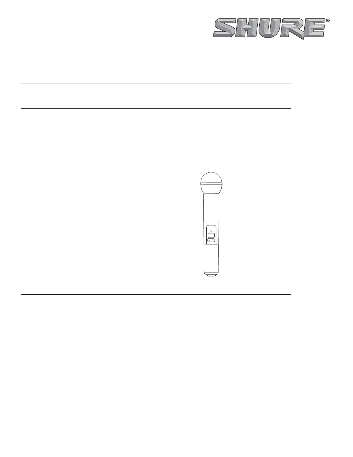
SLX2 WIRELESS HANDHELD TRANSMITTER
PRODUCT DESCRIPTION
The Shure Model SLX2 is a µP (microprocessor) controlled frequency agile UHF
handheld transmitter operating over the frequency range of 518 to 865 MHz (in eight
different 24 MHz-wide frequency bands). The transmitter will operate for a minimum of 8
hours using two "AA" alkaline batteries. The User Interface includes "mode" and "set"
buttons, and an LCD that displays battery status, group/channel, and transmitter/
receiver frequency synchronization. The SLX2 has a plastic enclosure, and utilizes an
internal antenna for optimum range and reliability. This product is intended for use in
entry-level presentation, installed, and performance markets.
25A1090
FEATURES
SLX
mute select
1. Frequency agile; microprocessor controlled. Model number extensio n determines frequency band of operation.
2. Minimum of 12 compatible systems per SKU in the U.S. Additionally, a minimum of 12 compatible systems in the top 50 U.S. markets across all three domestic SKU's (H5, J3, and L4).
3. Operating frequency programmable locally or from the receiver using a built-in IR link.
4. Designed for use with "AA" alkaline batteries (2 required). May also be used with rechargeable "AA"
batteries. Note: battery condition indicator is calibrated for alkaline batteries and may not be accurate with rechargeable types. Electrical reverse battery protection is included.
5. Minimum battery life of 8 hours with new "AA" alkaline batteries.
6. Designed for use with SM58, BETA 58, SM86, and BETA 87A&C microphone heads. Compatible with "active load" or standard heads (active load circuitry to be incorporated in heads).
7. Tone key squelch.
8. Power/Mute and Select buttons with LCD display for frequency group/channel selection and control. LED backlight for easy reading of LCD display.
9. Bicolor, green/red LED for power "on" and low battery, mute and infrared link indications.
10. Rugged plastic construction.
11 . Utilizes Shure Patented ARC (Audio Reference Companding) audio processing.
©2006, Shure Incorporated
25A1090 (Rev.3)
Page 2
DETAILED DESCRIPTION
1
2
SLX
3
4
mute select
5
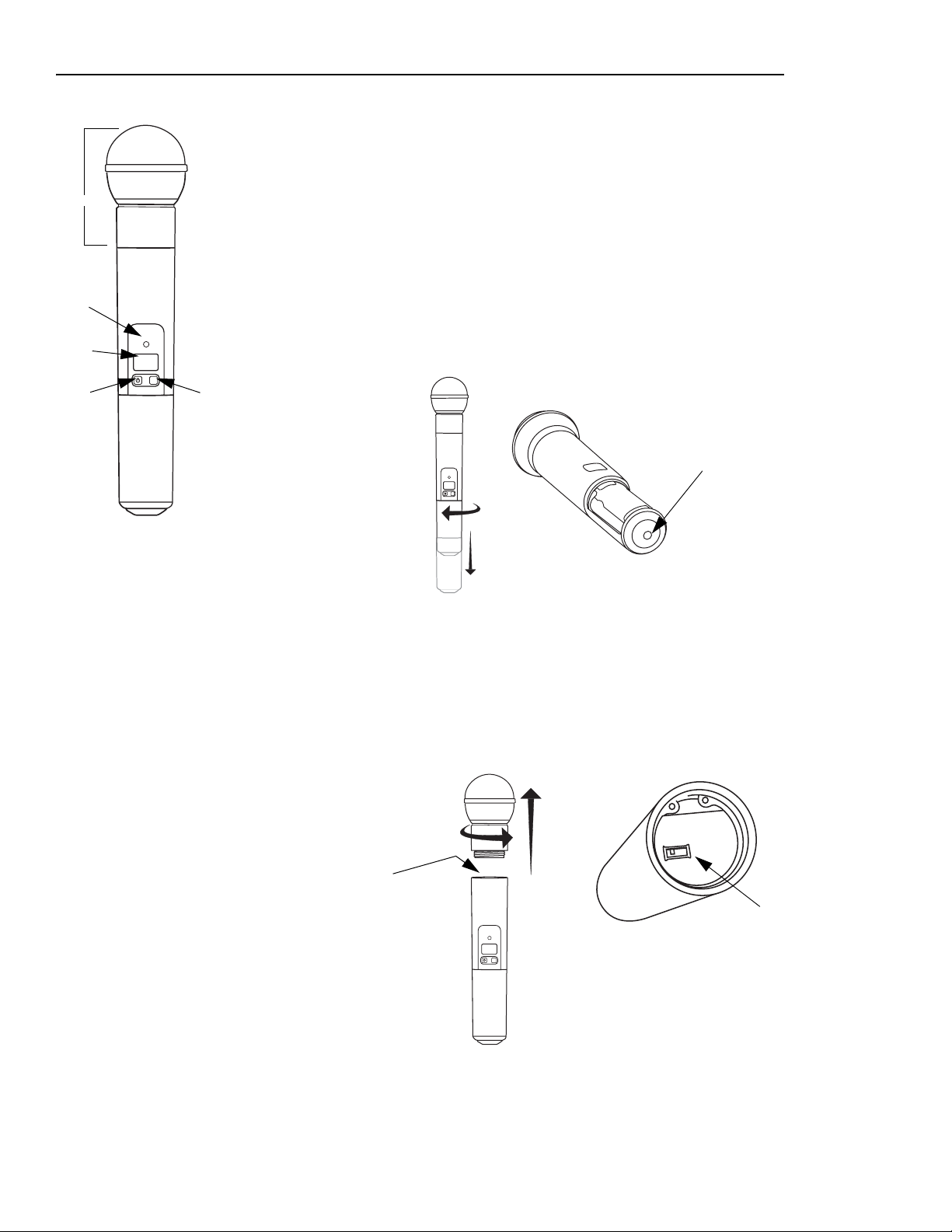
Features
1 Interchangeable microphone head (SM58 pictured)
2 Power / Infrared (IR) / Mute indicator
Green: ready
Amber: mute on
Flashing red: IR transmission in process
Glowing red: battery power low
Pulsing red: battery dead (transmitter cannot be turned off until batteries are changed)
3 LCD screen
4 On-off / mute switch
Press and hold to turn on or off. Press and release to mute or unmute.
5 Select switch
6IR port
Receives infrared beam to synchronize frequencies. When using multiple systems, only one
transmitter IR port should be exposed at a time.
SLX
mute select
6
Adjusting Gain
Access the gain adjustment switch a by unscrewing the head of the microphone.
Two gain settings are available on the SLX2. Choose a setting appropriate for vocal volume and for the performing environment. Use the tip of a pen or a small screwdriver to move the switch.
•
0dB:
For quiet to normal vocal performance.
•
–10dB
: For loud vocal performance.
BIAS
AUDIO
-10dB
0dB
a
b
SLX
25A1090 (Rev.3)
mute select
2
Page 3

a
MASTER LIST
GROUP
i8 i8
b
MASTER LIST
GROUP
i8 i8
Incompatible
CHANNEL
select
Incompatible
CHANNEL
select
SLX2 Transmitter Programming
Manually Select a Group and/or Channel
select
5
1. Press and hold the select button until the GROUP and CHANNEL displays begin to alternate.
a
2. To change the group setting, release the select button while GROUP is displayed
. While GROUP
is flashing, pressing select increases the group setting by one.
b
3. To change the channel setting, release the select button while CHANNEL is displayed
. While
CHANNEL is flashing, pressing select increases the channel setting by one.
Incompatible
MASTER LIST
CHANNEL
GROUP
i8 i8
Incompatible
MASTER LIST
CHANNEL
GROUP
i8 i8
Incompatible
MASTER LIST
CHANNEL
GROUP
i8 i8
Incompatible
MASTER LIST
CHANNEL
GROUP
i8 i8
Lock or Unlock Transmitter Settings
select
+
Press the mute/ and select buttons simultaneously to lock or unlock the transmitter settings. When
locked, the current settings cannot be changed manually. Locking the transmitter does not disable in-
frared synchronization.
Battery Status
Indicates charge remaining in transmitter batteries.
Master List Indicator
Indicates that a master list frequency is currently in use. No group or channel information is displayed.
Note: the transmitter cannot be used to change master list settings.
INCOMPATIBLE Frequency Warning
The INCOMPATIBLE warning indicates that the receiver and transmitter are transmitting on different
frequency bands. Contact your Shure retailer for assistance.
25A1090 (Rev.3)
3
Page 4
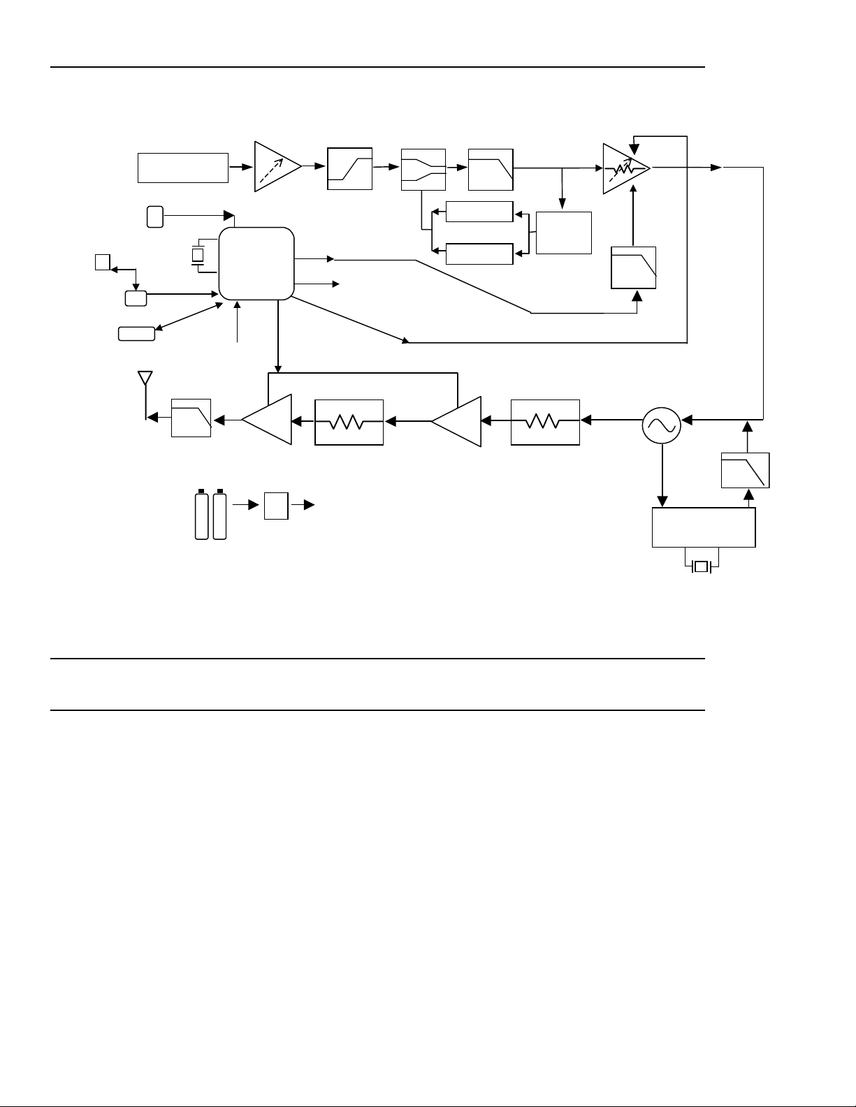
AUDIO/RF BLOCK DIAGRAM
A
Converte
A
A
A
IR
Photodetector
LCD
LCD
Driver
EPROM
Audio Input
(mic head)
32.768
LPF
Supply
Microcontroller
Channel
Select,
A Battery
User Gain
Control Switch
Tone Key
RF
mp
DC-DC
r
Preemphasis
Frequency
Synthesizer
control
RF Muting
Pad
0-4 dB (Band
dependent)
+5V DC
Source
VCA
Compressor
udio Muting
RF
mp
2-pole,
17kHz,
LPF
Limiter
Deviation Trim
and Tone Key
Sum Amp
RMS
Detector
Pad
0-4 dB (Band
dependent)
VCO (Carrier
Range)
Frequency
Synthesizer
Loop
Filter
16
MHz
CIRCUIT DESCRIPTION
AUDIO CIRCUIT DESCRIPTION
AUDIO SECTION
Audio enters the transmitter board through pin 4 of the mic-jack board connector (CON100).
Pin 2 of the connector provides 5 Vdc bias for the mic head. Pin 6 supplies the ground connection. The audio preamp (IC150-2) provides either 0 or 10 dB of gain (user switchable via
SW100). Capacitor C140 couples the signal into a pre-emphasis network formed by R140, R141,
and C141.
Next, the audio signal enters the patented Shure ARC™ processor. The main elements in this
section are the VCA (IC100-5) and the RMS Detector (IC100-4). The VCA, or Voltage Controlled
Amplifier, is a DC controlled amplifier. Following the VCA, the signal enters a 3-pole 17kHz lowpass filter stage (IC100-2) that protects the RMS detector from energy above the audio band.
Next, the signal is coupled to the RMS detector (IC100-1), which converts it to a DC voltage. A
+1 dB increase at the input to the detector produces a +6 mV increase at its output. The detector
output is fed to the compression threshold stage (IC150-2). This stage provides the transition
from uncompressed to compressed signal. At low levels, the audio is uncompressed because
diode D169 is turned off. As the AC level increases, the output of IC150-2 decreases enough to
turn the diode on. As D190 conducts, the compression ratio changes from 1:1 to 5:1. Once D190
is turned fully on, the audio compression ratio remains fixed at 5:1. An additional diode in the bias
25A1090 (Rev.3)
4
Page 5

network (D162) provides temperature compensation for changes in the VY, or "cut-in" voltage of
D190. After the compression threshold stage, the DC control signal is amplified by a 40 dB fixed-
gain stage (IC100-5). It is then sent to the VCA control voltage input (EC+).
Following the ARC™ processor section, the audio signal must pass through a muting network
consisting of R199, R200, C205, and Q205. A trim pot (TR200) allows the audio deviation level
to be set. Next, audio enters the tone key summing amp (IC150-4). Here, tone-key is added to
the audio before passing to the RF section for transmission. The tone key signal is used in the
receiver to provide audio output only when the tonekey signal is present with the transmitted signal; therefore, if the tone key or the transmitter is turned off, the receiver will be muted. The tone
key squelch will eliminate receiver noise associated with loss of the carrier, which usually sounds
like a "pop". The tone key signal is generated by a square wave from the mP (IC300). It is then
filtered by active filter stage Q185 and attenuated by R188/R189 (under µP control) before being
fed to the summing amplifier. The combined audio/tone-key signal is then sent to the VCO
through R504.
POWER SECTION
Two "AA" batteries supply power to the transmitter through FET Q410, which provides electrical reverse battery protection. Next, power enters switching boost converter IC400, which supplies regulated 5V power. To turn on the transmitter, SW325 shorts the base of Q480 to ground,
enabling the converter and powering up the unit. The microprocessor keeps Q480 disabled until
shutdown.
Power is turned off by a "shutdown" signal from the microprocessor, which can be initiated
manually by the user (by holding down SW325 for 2.2 seconds) or automatically by the system
(e.g., when the battery is too weak for proper operation). At this time, the microprocessor enables
Q480 and shuts down the converter. When the unit is off, Q480 and its bias circuitry draw less
than 30 µA, so the effect on battery life is negligible. The converter and microprocessor are disabled.
shutdown, and will not turn the system back on until a voltage greater than 2.25 V is present. The
hysteresis keeps the system in a controlled state when the batteries are low, and also helps prevent weak batteries from being used from the start.
RF CIRCUIT DESCRIPTION
frequency modulation. Processed audio enters the VCO through a passive "reflection" network
before being applied to the varactor diode (D500) through choke L503. The VCO is shielded to
prevent external RF fields from affecting its operation, and to help control radiated emissions of
its harmonics. Power for the VCO and PLL circuitry is supplied by the main 5 V regulator. Power
and signal lines in the VCO area are heavily decoupled and bypassed to remove noise.
range of approximately 1 to 4 volts. The VCO employs separate stages for the oscillator (Q502)
and buffer (Q501) to minimize phase noise and load pulling. The VCO output is isolated by capacitive and resistive dividers, before being applied to the frequency control pin of the PLL synthesizer (IC501) through C538. The synthesizer's internal circuitry divides the RF signal down as
necessary to achieve a tuning precision of 25 kHz. The synthesizer circuit contains a quartz-controlled reference oscillator operating from a 16 MHz reference crystal (Y801) that is adjusted by
means of trimmer CV501. The transmitter output frequency is user selectable in groups of compatible channels within each of the eight available bands. Frequency selection is made via microprocessor controller IC300, which interfaces with the user by means of the Group and
Channel switches, SW324 and SW325. The output of the synthesizer is a series of pulses that
are integrated by a passive loop filter consisting of C532, R514, C533, R513, and C531 to produce the control voltage signal.
of R602, C614, and L610. R600 and R603 provide base bias for the transistor, while R605 sets
its operating current. RF choke L600 provides power and decoupling for the stage, in conjunction
LOW BATTERY SHUT DOWN:
A software battery shutdown routine allows the battery supply to run down to 2.05 V before
RF SECTION
The system block diagram is shown above. The SLX2 uses a PLL system with direct carrier
The VCO has a tuning bandwidth of more than 30 MHz on all bands, with a tuning voltage
The VCO output is coupled to the RF buffer stage (Q600) by a matching network consisting
25A1090 (Rev.3)
5
Page 6
with C600 - C604. The collector of Q600 feeds the power amplifier stage via an impedance
matching network consisting of L602, C611, and C618.
The bias voltage for the RF power amplifier (Q601) is supplied by R601 and R604. Its operating current is controlled via emitter resistor R606. RF choke L601 provides power and decoupling
for the stage, in conjunction with C605-C609. For Japanese systems only, the output power is
trimmed via TR640. L603, C612, and L604 provide the output impedance matching into the low
pass filter, which consists of L604, L605, L606, C615, C616, and C617. The low pass filter output
couples to the battery antenna via C641 and L607. Connector CON640 and C613 are only used
for Japanese (JB) units. Coupling capacitor C610 is used to ensure that both batteries are driven
equally.
The transmitter is capable of delivering up to +15.0 dBm to the antenna (depending
on band and country). During transmitter power-up and frequency selection, the RF
output is muted by bringing the base of Q631 low, which removes bias from Q630
and shuts down power to the RF stages. The RF output is also muted during the
transmitter power-down sequence. This is done so that the carrier signal will not
interfere with other transmissions when the loop becomes unlocked.
DIGITAL CIRCUIT DIAGRAM
Backlight
LED
RF Band
DC Level
Battery DC
Level
Power Mute
Button
Select
Button
Softstart
Shutdown
Microprocessor
(Motorola
MC68HC908GR16)
Power LED
LCD Driver
(Rohm
BU9729k)
Sythesizer
(National
Semiconducter
LMX2335)
RF Power
Tonekey
Squarewave
LCD
VCO
25A1090 (Rev.3)
Infrared
Photodetector
(Sharp GP1U10X)
EEPROM
(MicroChip
93AA46 )
Audio Mute
Tonekey
Level
6
Page 7
DIGITAL SECTION
ACCESSING DIFFERENT MODES
ATE MODE
If TP_PB0 is held to TP_EGND, or logic level 0, at startup, the microcontroller will enter ATE
Mode. T o ensure proper operation, TP_P A0 and TP_P A1 should be held to TP_EGND at startup.
In ATE Mode, each band has a three test frequencies that are control led by the logic levels at
test points TP_PA0 and TP_PA1.
Frequency TP_PA0 TP_PA1
Low 00
Center 01
High 11
Test Frequencies (MHz) H5 J3 JB L4 P4 Q4 R5 S6
SLX2 Low 518.400 572.400 806.125 638.400 702.100 740.125 800.525 838.100
Center 529.500 583.500 807.500 649.500 714.000 746.325 810.275 851.300
High 541.800 595.800 809.750 661.800 725.900 751.875 819.800 864.800
RF BAND RESISTORS
Two resistors (RA and RB) are responsible to start the microcontroller in a RF band. They determine the voltage at test point TP_RFBAND.
This table shows R
reflect the operating RF band.
's and RB's reference designators and how the voltages at the test points
A
SLX Reference Designators
SLX2
R
A
R
B
R319 R320
This figure depicts the voltage divider feeding the microprocessor analog to digital converter.
.
25A1090 (Rev.3)
7
Page 8
This table shows the variant resistor values and resulting voltages at TP_RFBAND for each band.
RF BAND Rb TP_RFBAND(+/- 0.10V) H5 1.00k 0.30V J3 2.99k 0.76V L4 4.99k 1.10V R5 7.50k 1.41V S6 12.10k 1.81V P4 18.2k 2.13V Q4 30.1k 2.48V JB 49.9k 2.75V
Note: Voltages are calculated with a 3.30V (+/- 0.10V) reference from the power
supplies. If power section supports less than 3.30V, thresholds need to be adjusted.
µC DECISIONS BASED ON ANALOG VOLTAGES
Continuous Operation Battery Thresholds
BATTERY_A2D RF Level Display Logic Voltage (V)
Measured @ 3V
- dBC >= 2.25
block battery clips
- dBC < 2.25
- dBC < 2.14
-8 dBC < 2.05
Note: There is a dead battery lock voltage set at 2.30 Volts. If the transmitter is powered
on with a voltage of less than 2.30 Volts, the system will lock, forcing the user to either
recharge or replace the batteries. During the dead battery lock out, the battery gauge is
empty and the red led flashes.
25A1090 (Rev.3)
8
Page 9

NOTES
25A1090 (Rev.3)
9
Page 10

FUNCTIONAL TEST
REQUIRED TEST EQUIPMENT (OR APPROVED EQUIVALENT OR SUPERIOR MODELS):
Spectrum analyzer or power meter HP8590L/Agilent E4403B/Agilent E4407B Digital multimeter Fluke 87 Audio Analyzer HP 8903B Frequency Counter HP 53181/HP 5385A Power Supply Power Supply must be able to supply 3Vdc
Shielded test lead Shure PT1838F BNC (Male) to BNC (Male) cable (1) Shure PT1838A UA820 Antenna Frequency Dependent Audio Test Head PT1840
Brass Ring PT1838Y
LISTENING TEST
Before completely disassembling the transmitter, operate it to determine wether it is functioning normally and try to duplicate the reported malfunction. Refer to pages 2 and 3 for operating instructions, troubleshooting, and specifications.
Review any customer complaint or request, and focus the listening test on any reported problem. The following, more extensive, functional tests require partial disassembly.
FUNCTIONAL TEST
Refer to the Disassembly section to partially disassemble the transmitter for the following functional tests.
with an internal ammeter.
TEST SETUP
1. Remove the PCB from the handle.
2. Set gain switch to “0” dB.
3. Connect the (+) terminal of the power supply through a milliammeter to the (+) battery terminal and
the (-) power supply terminal to the (-) battery terminal.
4. Connect a DC Voltmeter across the power supply and set the power supply for 3Vdc.
5. Connect the audio analyzer to the microphone via the microphone test head (PT1840) as needed.
DISPLAY TEST
1. Power unit ON.
2. Verify that all display segments are displayed for approximately 2 seconds. This includes a full bat-
tery indication and "1818" displayed for group and channel.
REVERSE BATTERY PROTECTION TEST
1. Adjust power supply to -3.0 ± 0.1 V dc.
2. The current should be less than 0.5 mA.
VOLTAGE REGULATION TEST
With power applied properly, and the unit switched on, measure the DC voltages at the following test points. All test points are located on the top side of the PCB. Refere to the component diagram.
• TPBATT+ (Battery input) = 3 ± 0.2 Volts
• TP5V (Power Converter) = 5 ± 0.2 Volts
• TP3.3V (Power Converter) = 3.3 ± 0.2 Volts
• TPA1 (Audio Preamp) = 2.5 ± 0.2 Volts
• TPA3 (Tone Key Summing Amp (IC150 Pin 14)) = 2.5 ± 0.2 Volts
• TPVREF (IC100 Pin 5) = 2.5 ± 0.1 Volts
25A1090 (Rev.3)
CURRENT CONSUMPTION TEST
1. With +3V applied to the battery terminals and the unit powered on.
2. Verify the current drain is 130 ± 15mA.
10
Page 11

FREQUENCY RESPONSE TEST
1. Set the audio generator as follows:
•
Frequency = 1 kHz
• Amplitude = -20 dBu
• Filters = 30 kHz LPF
2. With the audio analyzer, probe TPA2 (top side), it should read -3.4dBu ± 0.5dB. Record this level
using the Ratio button. This level will be used as your reference level for the following test.
3. Change the generator's frequency to 100Hz and measure the level at TPA2 to be -2.2dB ± 0.2dB
relative to the 1kHz reference level.
4. Change the generator's frequency to 10kHz and measure the level at TPA2 to be +2.3dB ± 0.2dB
relative to the 1kHz reference level.
5. Disengage the Ratio button.
DISTORTION TEST
1. Set the audio generator frequency to 1kHz with an amplitude of -20.0dBu.
2. Activate the 30kHz LPF on the audio generator.
3. Measure the total harmonic distortion and noise (THD+N) at TPA2 to be less than 0.7%.
RADIATED RF OUTPUT POWER AND FREQUENCY STABILITY TEST
1. Choose any group and channel free of interference. Using a spectrum analyzer with the appropri-
ate-band UA820 antenna, measure the approximate near field radiated power as follows:
• SPAN=100 MHz
• REF LVL=10dBm
• FREQUENCY=(Look at tables on pages 18 thru 23)
2. Extend the UA820 away from the analyzer into the horizontal plane (straight out). Align the SLX2
antenna parallel to the UA820 as close as possible. Move the unit along the UA820 antenna until
you find a maximum peak.
3. Do a peak search and measure the power to be at least 2 dBm for H5, J3, L4, and P4 bands and at
least 0 dBm for Q4, R5, JB, and S6 bands.
4. Set SPAN to 200 KHz. Measure the frequency to be within +/- 3 kHz of the nominal frequency you
are testing. (See frequency tables on pages 19 to 24).
TONE KEY LEVEL TEST
1. Set Power Supply to 3.0VDC
2. Find transmitting carrier on the spectrum analyzer with a span of 200 kHz. Use the "Peak Search,
Marker Delta, Next Peak" soft-keys on the analyzer.
3. Measure the 32.768 kHz tone key level to be -21 dBc ± 1.5 dB.
4. Set Power Supply to 2.1 V (1 segment on LCD battery icon).
5. Measure the 32.768 kHz tone key level to be -14 dBc ± 1.5 dB.
OCCUPIED BANDWIDTH TEST (JB model only)
1. Set transmitter gain to maximum.
2. Set up the HP-8591E spectrum analyzer to measure Occupied Bandwidth with the following set-
tings:
• Percentage Power = 99.5%
• Channel Spacing = 250 kHz
• Bandwidth = 110 kHz
3. Connect the audio generator to TQG connector CON90. Use a 1 kHz tone with a level that gives -
23.47 dBu (52mV) at TPA3.
4. Increase the audio level by 36dB.
5. Measure Occupied Bandwidth to be less than 110 kHz.
ADJACENT CHANNEL POWER TEST (JB model only)
1. Set the spectrum analyzer, and audio input level to the same settings as stated in “Radiated RF
Output Power and Frequency Stability” and “Distortion Test”.
2. Measure Extended Adjacent Channel Power to be less than -60 dB.
25A1090 (Rev.3)
IF ALL TEST PASSED, THIS MEAN S T H E UN IT IS P R OP ERL Y FU NCT IONING, AND
NO ALIGNMENT IS REQUIRED.
11
Page 12

ASSEMBLY AND DISASSEMBLY
!CAUTION!
Observe precautions when handling this static-sensitive device.
EXPLODED VIEW
25A1090 (Rev.3)
I.D. # Description Part Number 0001 Cartridge 0002 Tuned PCB assembly 200--082 0003 PCB assembly, IR 190A098-01 0004 PCB, head board 190-057-03-34 0005 Contact 53F2039A 0006 Frame, internal 65B8467 0007 Retaining ring 30A1314 0008 bezel, painted/printed 65A8475B 0009 Pushbutton actuator, silicone 66A8070 0010 Battery cup, painted 65BA8451 0012 Shield cover, steel, plated 53A8590A 0014 3 pin interconnect 170A74 0015 PCB Screw, hi-lo #4 30J1245 0016 Handle assembly 95A9047B 0017 Battery holder assembly 95B9048 0018 Battery holder, Machine screw, #2–56 30D443E 0019 Nameplate, frequency 39--8466 0022 Battery cover assembly 95A9068
12
Page 13

SERVICE PROCEDURES
MEASUREMENT REFERENCE
NOTE: Audio levels in dBu are marked as dBm on the HP8903.
dB Conversion Chart
0dBu = 0dBm assuming the load = 600 ohms
Be aware that dBu is a measure of voltage and dBm
is a measure of power. The HP8903, for example,
should be labeled dBu instead of dBm since it is a
voltage measurement. These two terms are often
used interchangeably even though they have
REQUIRED TEST EQUIPMENT (OR APPROVED EQUIVALENT OR SUPERIOR MODELS):
Spectrum analyzer or power meter HP8591E/Agilent E4403B/Agilent E4407B Digital multimeter Fluke 87 Audio Analyzer HP 8903B RF Signal Generator HP 8656B or HP E4400B Frequency Counter HP 53181/HP 5385A Receiver Matching SLX4 Receiver 50 ohm, RG-174 BNC to open (stripped)
coaxial cable or "rocket launcher" tip (P/N
95A8278). For JB, Murata cable #
MXGS83RK3000 may be used.
Audio Test Head Shure PT1840
Brass Ring Shure PT1838Y
BNC (Male) to BNC (Male) Cable (2) Shure PT1838A DC Blocker Shure PT1838W XLR (Female) to Banana Plug Adapter Shure PT1841 20 dB Attenuator Shure PT1838T Toray non-inductive tuning tool - BLUE Shure PT1838K Toray non-inductive tuning tool - PINK Shure PT1838L
0dBV = 2.2 dBu
different meanings.
Shure PT 1824
25A1090 (Rev.3)
13
Page 14

ALIGNMENT PROCEDURE
Alignment and Measurement Procedure
The alignment procedure is sequential and does not change unless specified. Use RG58 or
other low loss 50 ohm cables for all RF connections. Type RG174 (thin) 50 ohm cables can be
used for short (e.g. 6 inch) runs. Keep RF test cables as short as possible. Include the insertion
loss of the cables and the connectors for all RF measurements. DC voltages are present at most
RF test points. Use DC blocks to protect the test equipment, if necessary. All audio analyzer filters should be OFF unless otherwise specified.
VOLTAGE REGULATION CHECK
With power applied properly, and the unit switched on, measure the DC voltages at the following test points. All test points are located on the top side of the PCB. Refere to the component
diagram.
T est Points Voltages
TPBATT+ (Battery input) 3 ± 0.2 Volts TP5V (Power Converter) 5 ± 0.2 Volts
TP3.3V (Power Converter) 3.3 ± 0.2 Volts
TPA1 (Audio Preamp) 2.5 ± 0.2 Volts
TPA3 (Tone Key Summing Amp,
2.5 ± 0.2 Volts
(IC150 Pin 14))
TPVREF (IC100 Pin 5) 2.5 ± 0.1 Volts
Frequency
Level
LOW GRP. 1 /
MID GRP. 4 /
HIGH GRP. 6 /
CH. 12
INITIAL SETUP
1. Proper adapters should be used to connect the test equipment.
2. Apply +3 V to the battery terminals with the proper polarity.
3. Set audio gain switch SW100 to "-10 dB".
4. Remove L641 to disengage the antenna (ALL EXCEPT JB).
5. Solder the center of a 50Ω unshielded test cable (PT1824) to the node between L606 and
L641, and the shield to ground.
6. Connect the audio generator output to the Mic Test Head input of the transmitter as
required.
7. Turn on the SLX2 by pressing and holding the POWER button, SW325
H5 J3 JB L4 P4 Q4 R5 S6
CH. 1
CH. 7
GRP. 1 /
CH. 1
GRP. 4 /
CH. 7
GRP. 6 /
CH. 12
RF TUNING
GRP. 1 /
CH. 5
GRP. 1 /
CH. 2
GRP. 5 /
CH. 4
GRP. 1 /
CH. 1
GRP. 4 /
CH. 7
GRP. 6 /
CH. 12
GRP. 14 /
CH. 1
GRP. 14 /
CH. 5
GRP. 15 /
CH. 10
GRP. 1 /
CH. 1
GRP. 1 /
CH. 5
GRP. 1 /
CH. 8
.
GRP. 4 /
CH. 1
GRP. 4 /
CH. 7
GRP. 2 /
CH. 11
GRP. 13 /
GRP. 14 /
GRP. 3 /
CH. 13
The removal of L641 (prevents antenna loading of output).
VCO Tuning:
1. Set transmitter to its LOW frequency as indicated in the table above.
2. WIth a DC meter probe TP_PLL_TV (top).
3. Tune CV500 to obtain 1.10-1.40 Vdc at TP_PLL_TV. For Q4 units, this voltage should
read between 1.45-2.25 Vdc. For JB units, this voltage should read between 1.75-2.05
Vdc.
4. Set the transmitter to HIGH frequency.
5. Verify voltage at TP_PLL_TV is less than or equal to 4.3 V DC.
CH. 1
CH. 7
25A1090 (Rev.3)
14
Page 15

FREQUENCY ALIGNMENT:
1. Set the transmitter to MID frequency (see table on page 14).
2. Connect the 50 Ω cable to a frequency counter.
3. Adjust variable capacitor CV501 until the frequency counter measurement matches the
appropriate frequency on the table below, ± 1 kHz. .
GROUP CODE FREQUENCY RANGE
H5 529.500 Mhz ± 1 kHz
J3 583.500 Mhz ± 1 kHz JB 807.500 Mhz ± 1 kHz L4 649.500 Mhz ± 1 kHz P4 714.000 Mhz ± 1 kHz Q4 746.325 Mhz ± 1 khz R5 810.275 Mhz ± 1 kHz S6 851.300 Mhz ± 1 kHz
RF OUTPUT POWER
The output power measurement ensures that the output signal is strong enough for
sufficient range when the system is in use. The output power measurement also verifies
tha the output power is not above the specified maximum level, to ensure compliance
with regulatory angencies’ standards.
1. RF output power is only adjustable on and JB units. Use RG58 (PT 1824) or any other low
loss 50 Ω cables for all RF connections.
2. Include the insertion loss of the cables and connectors in rf conductive power measurements.
3. Connect the RF output of the transmitter to a spectrum analyzer.
4. Set the spectrum analyzer center frequency to match the transmitter frequency.
5. Using a power meter or spectrum analyzer, verify the output power matches the range indicated in the table below. JB models can be adjusted at TR640.
GROUP Pout RANGE
H5 14 dBm ± 2 dB
J3 14 dBm ± 2 dB JB 7.0 - 10.8 dBm L4 14 dBm ± 2 dB P4 14 dBm ± 2 dB Q4 10 dBm ± 2 dB R5 13 dBm ± 2 dB S6 10 dBm ± 2 dB
6. Remove the BNC to unterminated test cable (PT1824) and replace L641 to reconnect the antenna.
DEVIATION ADJUSTMENT
Deviation must be set to make sure the companding systems between the transmitter and receiver correctly track each other. Th e le vel coming out of the transmitter’s audio compressor
must match the level going into the receiver’s audio expander. A fixed gain structure does not
ensure exact match, primarily because of variations in voltage-controlled oscillators (VCO’s).
USING A SLX4 RECEIVER
The following procedure requires a SLX4 receiver. It is recommended that a properly tuned receiver be used to perform the transmitter deviation adjustment.
25A1090 (Rev.3)
15
Page 16

RECEIVER SETUP
SLX4 RECEIVER AUDIO ANALYZER RF SIGNAL GENERATOR
Output: Unbalanced Measurement: AC level INT: FM
Gain: Maximum Filters: FM RATE: 1kHz
Toke Key: Disabled (R280) Low-Pass (30 kHz): ON Amplitude: -50 dBm
High-Pass (400 Hz): ON Deviation: 33 kHz
1. The SLX2 transmitter should be powered OFF for this procedure.
2. Connect the rf signal generator to any of the antenna inputs on the receiver. Make sure the
dc block is on the rf signal generator.
3. Set rf signal generator to the same frequency as the SLX2 transmitter.
4. Set rf signal generator modulation to 1 kHz and deviation to 33 kHz.
5. Set the amplitude of the rf signal generator to -50 dBm.
6. Disable tonekey by shorting the pads of R280 on the receiver.
DEVIATION REFERENCE LEVEL
1. Power ON the receiver.
2. Connect the unbalanced output of the SLX4 receiver to the audio analyzer input.
3. Note the voltage obtained. This is the deviation reference voltage.
4. Disconnect the rf signal generator from the SLX4.
5. Power OFF the receiver and remove the short on the R280 pads to enable tonekey.
RADIATED DEVIATION REFERENCE VOLTAGE
SLX2 TRANSMITTER AUDIO ANALYZER
Power: +3 Vdc Measurement: AC level
Atennuation: -10 dB Output: 1 kHz
Channel: See Table Filters:
Group: See Table Low-Pass (30 kHz): ON
High-Pass (400 Hz): ON
1. Connect the audio analyzer output to the Mic Test Head input of the transmitter.
2. Power ON the receiver.
3. Apply +3V to the battery terminals on the SLX2 and power up the unit.
4. Set the audio analyzer frequency to 1kHz.
5. Adjust the audio analyzer amplitude level (typically = -6.5 dBu) to obtain -13 dBu
at TPA1. (This corresponds to -9 dBu ± 2dB at the audio input (TPA0))
6. Adjust TR160 to obtain -3 dBu
± 0.15dB at TPA2.
.
7. Place the transmitter closer than 12 inch es (3 6 cm) to the receiver.
8. Connect both antennas on the receiver.
9. Connect the un
10.
Adjust TR200 until the ac voltmeter connected to th e receiver unbalanced output reads the
same
deviation reference voltage
balanced output of the receiver to the audio analyzer.
± 0.1dB, as measured above.
(TR200 adjusts the deviation for 33 kHz, 100% modulation.)
If successful in the alignment of the unit, assemble it back together as indicated on
page 12. If not successful refere to our Bench Checks section on page28.
± 0.1dB
25A1090 (Rev.3)
16
Page 17

NOTES:
25A1090 (Rev.3)
17
Page 18

FREQUENCY TABLES
H5: 518.000 - 542.000 MHz
Preprogrammed frequencies in total: > 120
Group 1 Group 2 Group 3 Group 4 Group 5 Group 6 1 518.400 519.250 518.200 519.775 519.100 518.425 2 521.500 520.500 519.675 522.500 521.225 520.400 3 523.575 522.225 520.800 524.200 522.550 523.425 4 525.050 524.725 522.450 525.600 524.575 525.475 5 527.425 526.350 523.750 526.700 526.900 527.775 6 529.200 527.550 526.200 528.250 530.500 531.675 7 532.450 530.800 528.325 529.500 531.750 533.800 8 533.650 532.575 532.225 533.100 533.300 536.250 9 535.275 534.950 534.525 535.425 534.400 537.550 10 537.775 536.425 536.575 537.450 535.800 539.200 11 539.500 538.500 539.600 538.775 537.500 540.325 12 540.750 541.600 541.575 540.900 540.225 541.800
Explanation of group
content
Full Range even
distribution for each
TV-CH (option 1)
Full Range even
distribution for each
TV-CH (option 2)
Full Range max. # of
frequencies for CH22 (option 1)
Full Range max. # of
frequencies for CH23 (option 1)
Full Range max. # of
frequencies for CH24 (option 1)
Full Range max. # of
frequencies for CH25 (option 1)
J3: 572.000 - 596.000 MHZ
Preprogrammed frequencies in total: > 120
Group 1 Group 2 Group 3 Group 4 Group 5 Group 6 1 572.400 573.250 572.200 573.775 573.100 572.425 2 575.500 574.500 573.675 576.500 575.225 574.400 3 577.575 576.225 574.800 578.200 576.550 577.425 4 579.050 578.725 576.450 579.600 578.575 579.475 5 581.425 580.350 577.750 580.700 580.900 581.775 6 583.200 581.550 580.200 582.250 584.500 585.675 7 586.450 584.800 582.325 583.500 585.750 587.800 8 587.650 586.575 586.225 587.100 587.300 590.250 9 589.275 588.950 588.525 589.425 588.400 591.550 10 591.775 590.425 590.575 591.450 589.800 593.200 11 593.500 592.500 593.600 592.775 591.500 594.325 12 594.750 595.600 595.575 594.900 594.225 595.800
Explanation of group
content
Full Range even
distrobution for each
TV-CH (option 1)
Full Range even
distrobution for each
TV-CH (option 2)
Full Range max. # of
frequencies for CH31 (option 1)
Full Range max. # of
frequencies for CH32 (option 1)
Full Range max. # of
frequencies for CH33 (option 1)
Full Range max. # of
frequencies for CH34 (option 1)
25A1090 (Rev.3)
18
Page 19

JB: 806.000 - 810.000 MHZ
Preprogrammed frequencies in total: 21
Group 1 Group 2 Group 3 Group 4 Group 5 Group 6 1 806.250 806.375 806.125 806.500 806.125 806.250 2 807.500 808.625 807.375 807.375 807.375 807.250 3 809.625 809.750 809.500 808.625 808.375 808.500 4 809.625 809.750 809.375
Explanation of group
content
Full Range max. # of
compatible
frequencies (option
1)
Full Range max. # of
compatible
frequencies (option
2)
Full Range max. # of
compatible
frequencies (option
3)
Full Range max. # of
compatible
frequencies (option
4)
Full Range max. # of
compatible
frequencies (option
5)
L4: 638.000 - 662.000 MHZ
Preprogrammed frequencies in total: > 120
Group 1 Group 2 Group 3 Group 4 Group 5 Group 6 1 638.400 639.250 638.200 639.775 639.100 638.425 2 641.500 640.500 639.675 642.500 641.225 640.400 3 643.575 642.225 640.800 644.200 642.550 643.425 4 645.050 644.725 642.450 645.600 644.575 645.475 5 647.425 646.350 643.750 646.700 646.900 647.775 6 649.200 647.550 646.200 648.250 650.500 651.675 7 652.450 650.800 648.325 649.500 651.750 653.800 8 653.650 652.575 652.225 653.100 653.300 656.250 9 655.275 654.950 654.525 655.425 654.400 657.550 10 657.775 656.425 656.575 657.450 655.800 659.200 11 659.500 658.500 659.600 658.775 657.500 660.325 12 660.750 661.600 661.575 660.900 660.225 661.800
Explanation of group
content
Full Range even
distribution for each
TV-CH (option 1)
Full Range even
distribution for each
TV-CH (option 2)
Full Range max. # of
frequencies for CH42 (option 1)
Full Range max. # of
frequencies for CH43 (option 1)
Full Range max. # of
frequencies for CH44 (option 1)
Full Range max. # of
compatible
frequencies (option
6)
Full Range max. # of
frequencies for CH45 (option 1)
25A1090 (Rev.3)
19
Page 20

P4: 702.000 - 726.000 MHZ
Preprogrammed frequencies in total:
148
12 12 12 10 10 9 9 10 11 Group 1 Group 2 Group 3 Group 4 Group 5 Group 6 Group 7 Group 8 Group 9 1 702.200 703.750 703.650 702.750 703.750 702.100 704.775 702.300 703.000 2 704.200 705.975 705.650 704.500 705.750 704.025 706.225 704.975 706.025 3 707.200 707.200 708.650 705.750 708.250 705.500 710.500 706.775 708.000 4 709.425 708.850 710.875 708.250 711.750 708.500 712.025 709.100 710.300 5 711.000 710.950 712.450 711.250 714.500 710.100 714.225 710.300 712.225 6 713.675 712.425 715.125 712.500 715.750 712.025 716.900 712.225 716.000 7 715.575 714.325 717.025 715.250 718.750 713.500 718.500 714.775 717.100 8 717.050 717.000 718.500 718.750 721.250 717.300 720.775 716.700 719.000 9 719.150 718.575 720.600 721.250 722.500 725.300 725.300 724.000 720.225 10 720.800 720.800 722.250 723.250 724.250 725.900 722.775 11 722.025 723.800 723.475 724.700 12 724.250 725.800 725.700
Explanation
of group
content
Full Range
max. # of
compatible
frequencies
(option 1)
Full Range
max. # of
compatible
freque-cies
(option 2)
Full Range
max. # of
compatible
frequencies
(option 3)
France
preferred:
User Group A
(option 1)
France
preferred:
User Group A
(option 2)
France
preferred:
User Group B
(option 1)
France
preferred:
User Group B
(option 2)
France
preferred:
User Group C
(option 1)
France
preferred:
User Group C
(option 2)
P4: 702.000 - 726.000 MHZ CONTINUED
665108108 Group 10 Group 11 Group 12 Group 13 Group 14 Group 15 Group 16
1 702.200 710.200 718.200 702.550 702.100 702.700 702.500 2 703.300 711.300 719.300 705.600 704.700 704.700 705.500 3 704.700 712.700 720.700 707.500 710.300 709.450 707.000 4 705.800 713.800 721.800 709.000 712.400 711.500 712.200 5 707.675 715.675 723.675 711.500 714.000 714.500 714.100 6 708.775 716.775 715.100 716.500 716.550 716.400 7 717.000 719.400 719.900 719.500 8 720.000 721.300 722.000 722.200 9 723.500 724.700 10 725.900 725.900 11 12
Explanation of
group content
Optimized TV
channels: TV ch.
50 702-710 MHz
Optimized TV
channels: TV ch.
51 710-718 MHz
Optimized TV
channels: TV ch.
52 718-724 MHz
Compatible setup
for use with
PSM400-P3 (P4 >
P3)
Compatible setup
for use with
PSM400-P3 (P4 =
P3)
Compatible setup
for use with
PSM400-HF (P4 >
HF)
Compatible setup
for use with
PSM400-HF (P4 =
HF)
25A1090 (Rev.3)
20
Page 21

Q4: 740.000 - 752.000 MHZ
Preprogrammed frequencies in total:
36
Group 1 Group 2 Group 3 Group 4 1 740.125 740.125 740.125 740.125 2 741.500 741.950 741.225 740.800 3 743.375 743.500 742.925 741.825 4 744.600 745.675 744.325 743.075 5 746.325 747.400 745.425 745.125 6 748.500 748.625 746.875 746.575 7 750.050 750.500 748.925 747.675 8 751.875 751.875 750.175 749.075 9 751.200 750.775 10 751.875 751.875
Explanation
of group
content
Full Range
max. # of
compatible
frequencies
(option 1)
Full Range
max. # of
compatible
freque-cies
(option 2)
Full Range
max. # of
compatible
frequencies
(option 3)
Full Range
max. # of
compatible
frequencies
(option 4)
25A1090 (Rev.3)
21
Page 22

R5: 800.000 - 820.000 MHZ
Preprogrammed frequencies in total:
113
1111119899
Group 1 Group 2 Group 3 Group 4 Group 5 Group 6 Group 7
1 801.250 801.225 800.950 800.525 801.475 800.600 800.650 2 804.825 804.800 802.950 801.925 803.025 802.050 803.125 3 806.975 806.950 804.325 803.650 805.800 804.275 804.450 4 808.800 808.775 806.425 804.850 806.950 805.750 806.150 5 810.325 810.300 808.050 807.400 809.125 806.850 807.250 6 811.550 811.525 809.275 808.525 810.575 808.550 808.725 7 813.175 813.150 810.800 810.275 811.725 809.875 810.950 8 815.275 815.250 812.625 811.550 813.800 812.350 812.400 9 816.650 816.625 814.775 813.775 813.450 813.500 10 818.650 818.625 818.350 11 819.750 819.800 819.775
Explanation of group content
Full Range max. #
of comp. Frequencies & FIN
/ NOR / DEN
(option 1)
Full Range max. #
of comp.
Frequencies &
FIN / NOR / DEN
(option 2)
Full Range max. #
of comp.
Frequencies &
FIN / NOR / DEN
(option 3)
Germany
preferred: User
Group 4 800-814
MHz (option 1)
Germany
preferred: User
Group 4 800-814
MHz (option 2)
Sweden
preferred: 800814 MHz (option
1)
Sweden
preferred: 800814 MHz (option
2)
R5: 800.000 - 820.000 MHZ CONTINUED
7738686 Group 8 Group 9 Group 10 Group 11 Group 12 Group 13 Group 14
1 806.000 806.025 801.400 800.900 801.200 803.850 806.150 2 807.100 807.425 808.300 802.100 803.800 807.000 811.650 3 808.500 808.525 816.400 806.200 805.900 809.700 814.400 4 809.600 810.400 809.300 807.000 811.050 816.500 5 811.475 811.500 814.100 809.200 813.900 817.450 6 812.575 812.900 816.100 811.700 816.500 819.300 7 813.975 814.000 817.200 817.600 8 819.600 819.500 Explanation of
group content
Compatible setup
for use with
EUT-TL-TV (R5
> TL-TV)
Compatible setup
for use with
PSM400-MN (R5 >
MN)
Compatible setup
for use with
PSM400-MN (R5 =
MN)
Compatible setup
for use with
PSM200-R8 (R5 >
R8)
Compatible setup
for use with
PSM200-R8 (R5 =
R8)
Compatible setup
for use with
EUT-TL-TV (R5
> TL-TV)
Compatible setup
for use with
PSM400-MN (R5 >
MN)
25A1090 (Rev. 3)
22
Page 23

S6: 838.000–865.000 MHZ
Preprogrammed frequencies in total:
119
13 13 13 6 3 3 6 6 Group 1 Group 2 Group 3 Group 4 Group 5 Group 6 Group 7 Group 8
1 838.200 838.150 838.550 854.200 855.475 855.075 854.750 854.750 2 841.450 839.375 839.775 855.300 857.425 857.775 855.850 855.850 3 843.275 841.300 841.700 856.700 860.600 860.725 857.250 857.250 4 846.225 842.475 842.875 857.800 858.350 858.350 5 847.350 846.400 846.800 859.675 860.225 860.225 6 850.125 848.025 848.425 860.775 861.325 861.325 7 852.575 850.025 850.425 8 854.575 852.475 852.875 9 856.200 855.250 855.650 10 860.125 856.375 856.775 11 861.300 859.325 859.725 12 863.225 861.150 861.550 13 864.450 864.400 864.800 Explanation
of group
content
Full Range max.
# of compatible
frequencies
(option 1)
Full Range max.
# of compatible
frequencies
(option 2)
Full Range max.
# of compatible
frequencies
(option 3)
BEL / TUR
preferred:
opt. TV ch.69
854-862 MHz
U.K. preferred:
"CH69 Coordinated" SET
1
U.K. preferred:
"CH69 Coordinated" SET
2 or SET 3
U.K. preferred:
"Co-ordinated
frequencies"
INDOORS
S6: 838.000–865.000 MHZ CONTINUED
U.K. preferred:
"Co-ordinated
frequencies"
OUTDOORS
(option 1)
621013979 Group 9 Group 10 Group 11 Group 12 Group 13 Group 14 Group 15
1 854.425 863.200 838.200 838.900 838.100 838.700 838.400 2 855.525 864.500 839.900 842.600 841.100 842.800 840.600 3 857.400 841.000 845.900 842.700 844.800 842.100 4 858.500 842.375 847.500 847.000 846.300 844.700 5 859.900 844.400 848.600 849.200 847.400 846.600 6 861.000 846.100 850.100 850.400 849.200 848.100 7 847.350 852.100 852.500 851.300 850.700 8 849.400 853.300 854.100 851.850 9 851.800 855.100 855.300 853.700 10 853.200 857.210 11 858.650 12 859.800 13 861.900 Explanation of
group content
U.K. preferred:
"Co-ordinated
frequencies"
OUTDOORS
(option 2)
European
harmonized band:
optimized for 863 865 MHz
Compatible setup
for use with
EUT-TW-TZ (S6
> TW-TZ)
Compatible setup
for use with
EUT-VR-VT (S6
> VR-VT)
Compatible setup
for use with
PSM400-KE (S6 >
KE)
Compatible setup
for use with
PSM400-KE (S6 =
KE)
Compatible setup
for use with
PSM200-S5 (S6 >
S5)
25A1090 (Rev. 3)
23
Page 24

AGENCY APPROVALS
Note: Consult Global Compliance for latest applicable standards
FCC (H5, J3, L4) - Part 74
IC (H5, J3, L4) - RSS-123
ETS (H5, J3, L4, P4, Q4, R5, S6,) - EN 300 422 and EN 301 489
TELEC (JB) - RCR STD-22
PRODUCT PERFORMANCE CHARACTERISTICS
SPECIFICATION Value
Operating Frequency (H5) 518.100 to 541.900 MHz Operating Frequency (J3) 572.100 to 595.900 MHz Operating Frequency (L4) 638.100 to 661.900 MHz
Operating Frequency (P4) 702.100 to 725.900 MHz Operating Frequency (Q4) 740.100 to 751.900 MHz Operating Frequency (R5) 800.100 to 819.900 MHz Operating Frequency (S6) 838.100 to 864.900 MHz
Operating Frequency (JB) 806.125 to 809.750 MHz
Number of User Selectable Channels See frequency table
Type of Emission 120KF3E
Oscillator PLL-controlled synthesizer
RF Conducted Power Output Band Dependent (See Table 1)
Tonekey Signal 32.768kHz
Maximum FM Deviation 38 kHz
Dynamic Range > 100 dB Total Harmonic Distortion < 0.7% (38 kHz deviation, 1 kHz) Audio Adjustment Range -10, 0, or +15 dB; user selectable
Operating Voltage 3V (2 x AA; alkaline or rechargeable)
Power Consumption 130mA ± 15mA @ 3V
Battery Life > 8 hrs (alkaline batteries)
JB MODEL (CHANGES FROM R5 MODEL)
Operating Frequency 806 to 810 MHz
Number of User Selectable Channels 16 (125 kHz Spacing)
Frequency Stability ± 10 ppm
Reference FM Deviation1 kHz audio level 5 kHz -23.47 dBu (52 mV) at TPA0
Output Power See Table 1
25A1090 (Rev.3)
24
Page 25

NOTES
25A1090 (Rev.3)
25
Page 26

PRODUCT SPECIFICATIONS
MECHANICAL
Overall Dimensions
64 mm x 109 mm x 19 mm (2.50 x 4.30 x 0.75 in.)
Weight
73 grams (2.6 oz), without batteries
Housing
Molded ABS case and battery cover
GENERAL
Frequency Range and Transmitter Output Level
Band Range Transmitter output H5 J3 L4 P4 R5 S6 JB Q4
518–542 MHz 30 mW/15 dBm
572–596 MHz 30 mW/15 dBm
638–662 MHz 30 mW/15 dBm
702–726 MHz 30 mW/15 dBm
800–820 MHz 20 mW/13 dBm
838–865 MHz 10 mW/10 dBm
806–810 MHz 10 mW/10 dBm
740–752 MHz 10 mW/10 dBm
NOTE: This Radio apparatus may be capable of operating on some frequencies not authorized in your region. Please contact your national authority to obtain information on authorized
frequencies for wireless microphone products in your region.
Operating Range Under Typical Conditions
100m (300 ft.)
Note: actual range depends on RF signal absorption, reflection, and interference
Audio Frequency Response (+/– 2 dB)
Minimum: 45 Hz
Maximum: 15 kHz
Total Harmonic Distortion (ref. +/– 38 kHz deviation, 1 kHz tone)
0.5%, typical
Signal-to-Noise Ratio
>100 dB A-weighted
Operating Temperature Range
–18°C (0°F) to +50°C (+122°F)
Note: battery characteristics may limit this range
Transmitter Audio Polarity
Positive pressure on microphone diaphragm (or positive voltage applied to tip of WA302
phone plug) produces positive voltage on pin 2 (with respect to pin 3 of low impedance output)
and the tip of the high impedance 1/4-inch output.
Gain Adjustment Range
25 dB
Audio Input Level
-5 dBV maximum at mic gain position
+10 dBV maximum at 0 dB gain position
+20 dBV maximum at -10 dB gain position
Input Impedence
1 MΩ
25A1090 (Rev.3)
26
Page 27

ENVIRONMENTAL
RF Transmitter Output
30 mW maximum (dependent on applicable country regulations)
Dimensions
254 mm H x 51 mm dia. (10x2 in) including SM58 cartridge
Weight
375.6 grams (13.25 oz) without ba tt eries
Housing
Molded ABS handle and battery cup
Power Requirements
2 “AA” size alkaline or rechargeable batteries
Battery Life
>8 hours (alkaline)
Temperature Storage
7 days at +165 F (+74 F) degrees, unpackaged.
7 days at -20 F (-29 C) degrees, packaged.
After each 7-day storage period, units must be allowed to stabilize for 24 hours before testing.
Units must operate per Section V.
Temperature Cycling
5 cycles from -20 F (-29 C) degrees to +165 F (+74 C) degrees. Allow 24 hours for stabilization
before testing. Units must operate per Section V specifications mechanically and electrically.
Operational Temperature
Operate units as described in Section V at +0 F (-18 C) and +135 F (+57.9 C) degrees. Allow
three hours for stabilization of each temperature before testing. Units must operate per Section V specifications.
Steady State Humidity
Perform a 10 day test at 90% RH at room temperature. Evaluate units for visual and mechanical defects after 1, 3, 5, 7, and 10 days. At the end of the 10-day period allow the units to
recover for 24 hours. Units must pass Section V specifications.
Operational Humidity
Operate units as described in Section V at 90% RH at room temperature.
Allow two days for stabilization.
Moisture Resistance
Perform a 10-day test at 90% to 98% RH with temperature cycled between +14 F (-10 C) and
+150 F (+65 C) degrees. Allow the units to recover for 24 h ours. Product must meet Section
V specifications.
Mechanical Shock
Handheld Drop Test: Drop product from a height of 6' on to a hardwood floo r for a total of 10
drops. The unit must pass Section V specifications.
Stand Drop Test: Place product on a stand with the appropriate size swivel adapter. Drop unit
from a height of 5' onto a hardwood floor for total of 10 drops. The product must meet Section
V specifications.
Electrostatic Discharge
Product will be subjected up to a ± 15 kV air discharge an d ± 4 kV contact discharge. Units
must operate per Section V specifications.
25A1090 (Rev.3)
27
Page 28

TROUBLESHOOTING
Servicing will be more efficient when the history of the unit is known and can be taken into account. The service strategy should be different when a unit fails on the production line than when
it fails in the field, because if it fails on the line there is a possibility of incorrect or missing parts.
If the unit has failed in the field, check for signs of tampering or hand soldering that could indicate
that the customer has modified the unit or has attempted to repair it.
PRELIMINARY TESTS
1. Install two fresh "AA" batteries and turn the unit on. Verify normal display operation. Set
the unit to the lowest frequency in the group.
2. Observe the radiated output on a spectrum analyzer by holding it near the analyzer's
antenna. Measure the frequency and RF power output level and verify that they are within
expected limits.
3. Speak into the microphone. Observe the modulation on the spectrum analyzer display and
listen to the audio output on a matching SLX4 receiver tuned to the same channel; preferably the customer's unit, if this is a field return. Check for normal audio level. Listen for distortion, noise, or any unusual sounds.
4. Change the frequency to the highest frequency in the group. Repeat steps 2 and 3 above
and verify that operation is normal.
RF FREQUENCY OR SIGNAL PRESENCE PROBLEMS
If there is no carrier present at the transmitter antenna port or measured RF power is unusually
low, check the earlier stages to verify decent continuity of the signal path. An amplifier stage or
filter may have a part placement error or other defect. Usually the first step is to visually examine
the board for skewed / missing parts before going in with a probe. If there is no signal out of the
VCO output then check the control voltage at TP_PLL_TV when the transmitter is set at the lowest channel in the group. If the voltage is not tunable into the 1.1-1.4 V window but can be tuned
to a lower or higher voltage, this means the VCO might be built for the wrong band or has a wrong
part.
Check the values of the caps C522, C523, C528, C525, C534, and inductor L505 one by one
and try to tune into the window. (Note that these caps are Low-ESR series!) If the voltage at
TP_PLL_TV is 0 V and does not respond to tuning CV500, the loop is unlocked.
Check Y500 for a 16 MHz oscillation by setting the analyzer to CENTER FREQ=16 MHz, REF.
LEVEL=-40 dBm, SPAN=1 MHz. Hold the probe right above the cryst al and look for a spike-like
signal. If one is present, check the parts in the VCO, including parts other than the capacitors
mentioned above to see if anything is not soldered correctly.
Check bias voltages on the transistors to verify that they are powered and biased correctly. If
an oscillation exists at the output and is close to the nominal center frequency (within 100 kHz)
but cannot be tuned to the +/- 3 kHz window via CV501, check the value of the caps C536 and
C537.
Check that the trimmer CV501 is soldered correctly.
25A1090 (Rev.3)
LOW RF OUTPUT POWER
If RF signal is present at the right frequency with low power, compare the RF power measurements with a known good board at various points moving from the antenna backwards towards
the VCO. Look for signal discontinuities in the path (sudden large drop in measured power by
more than a few dB).
Check the board visually for missing/skewed parts. Try to confine the problem to a specific circuit segment, and then check solder connections and part values or DC voltages for error. If the
power out of the VCO is very low, check the bias voltages on the transistors and the values of
L502, C551, C543, C530.
EXCESSIVE CURRENT DRAIN
Try isolating different sections of the transmitter, such as the RF, Audio, and Digital circuits. Look for reversed polarity capacitors, wrong resistor values, poorly soldered components, and shorted traces.
28
Page 29

DEVIATION PROBLEMS
If TR200 can't be adjusted to obtain proper deviation, try to isolate the problem to the Audio
or RF section. To check the RF section, set the transmitter frequency to the frequency listed in
T able 1.2 in Section IV and verify that the tuning voltage of the VCO is correct. To check the audio
section, apply -10dBu at 1kHz to TPA0. Set the gain to "0 dB". Check for audio with a scope at
TPA1. The level should be approximately 0dBu. Next, check the audio level at TP A2 for -0.8dBu.
Finally, check the level at pin 14 of IC150-4. If the level is correct, check the values of R504,
R510, R511, and C513-C5126 in the VCO area. If there is no audio, or the level is wrong, the
problem is in the audio section. Trace backwards through the audio stages until you find the problem.
MICROCONTROLLER TROUBLESHOOTING
This paragraph describes what digital signals need to be seen to have audio running through
a SLX system. The first thing that needs to be checked is, if the microcontroller is running its software.
If you see numbers or only fragments of numbers on the display after the unit has powered up, the microcontroller is running fine. Fragments of numbers in the display point to an open LCD driver pin or an intermittent LCD panel connection.
To test the microcontroller for normal operation, please test the following pins and conditions.
Microcontroller Pin Number Net Name Condition
1 to gnd ~RST 3.3V 4 to gnd ~IRQ 3.3V
Across 10 and 9 VDD and VSS 3.3V
Across 20 and 21 VDDAD and
3.1V
VSSAD
Across 28 and 29 VDDA and
3.3V
VSSA
31 to gnd OSC2 Square Wave
f0=32768Hz
The turn on procedure of the SLX transmitters includes several stages:
T = 0.000s: The power is turned on (soft switch). 5V and 3.3V are established
approximately at the same time.
T = 0.480s: 32.768KHz crystal oscillates in a stable manner (~300ms) and internal reset
cycle (~180ms) is over. From now software gets executed.
T = 0.???s: Microcontroller pin 5 (RF_VCC_OFF) goes from 5V to 0V. Synthesizer is
powered on.
T = 0.???s: PLL data gets sent. You should see a signal similar to the graphic on an oscilloscope.
25A1090 (Rev.3)
29
Page 30

(1) = PLL_LE @ pin 34, (2) = PLL_DATA @ pin 35, (3) = PLL_CLOCK @ pin 36
T = 1.800s: Microcontroller pin 6 (RF_GND_ON) goes from 0V to 5V. RF carrier gets
unmuted.
T = 2.000s: Tone-key is turned on. You will see a square wave (Vpp = 5V, f0=32768Hz) at
microcontroller pin 18 (TONEKEY_SQUARE).If these stages can be captured with the scope,
the microcontroller did its part to let audio go through the system. If audio is still not being
transmitted, please involve RF spectrum analyzer and oscilloscope to debug the RF and audio
stage of the transmitter.
25A1090 (Rev.3)
30
Page 31

REPLACEMENT PARTS
PRODUCT CHANGES
PARTS DESIGNATIONS
The following comments apply to the parts list and the schematics:
Resistors: Unless otherwise noted, all resistors are surface-mount with 1/10 W rating and 1% tolerance.
Capacitors: Unless otherwise noted, non-polarized capacitors are surface-mount NPO dielectric types with a 100 V capacity and a 5% tolerance, and polarized capacitors are tantalum types.
SLX2 MODEL VARIATION
COUNTRY
CODE
FREQUENCY
RANGE
COUNTRY
DESIGNATION
SLX2
RF-AUDIO
PC BOARD NUMBER
H5 554-590 MHz U.S.A. and CANADA 200H510304
J3 572-596 MHz U.S.A. and CANADA 200J310304 L4 638-662 MHz U.S.A. and CANADA 200L410304 P4 702-726 MHz EUROPE / CHINA 200P410304
Q4 740-752 MHz KOREA 200Q410304
R5 800-820 MHz EUROPE 200R510304 S6 838-865 MHz GREAT BRITAIN 200S610304 JB 806-810 MHz JAPAN 200JB10304
SLX2 HARDWARE REPLACEMENT PARTS
Reference
Designation
A1 IR Assembly 190A10302
IR Detector 40kHz 188A617 3 Pin Male Connector Strip 170A76
A2 Handle Assembly 95A9047B
Aluminum ID Ring 53A8594 IR Bezel 65A8474
A3 Battery Cover Assembly 95A9068
Foam Pad 36A814
A4 Battery Holder Assembly 95B9048 MP1 Headboard PCB 190-057-03-34 MP2 Copper Contacts 53F2039A MP3 3 Pin Interconnect Strip 56E8074 MP4 Retaining Ring 30A1314 MP5 Internal Frame 65B8467
Description Shure
Part Number
25A1090 (Rev.3)
31
Page 32

MP6 Bezel 65A8475B MP7 Pushbutton Switch Actuator (Power/Mute/Select) 66A8070 MP8 Battery Cup 65BA8451 MP9 Frequency Nameplate 39__8466
MP10 PCB Screw 30J1245B
MP11 Battery Nest Screws 30D443E MP12 RF Shield Cover 53A8590A MP13 LCD Holder/Backlight 65A8452 MP14 LCD Bezel 53A8573B MP15 LCD 95A8991 MP16 LCD Zebra Connector 80A8257 MP17 Compression Pad (For Positive Battery Contact) 38D189
Provide
Frequency Code
In The Space
SLX2 REPLACEMENT PARTS (TOP)
Reference
Designation
C100 Capacitor, Tantalum, SMD1206, 15uF, 10V, 10% 151AC156KA
C162 Capacitor, Tantalum, SMD1411, 10uF, 16V, 10% 151AD106KB
C531 Capacitor, Tantalum, SMD1206, 0.1uF, 35V, 10% 151AG104KA
C432, 548, 549 Capacitor, Tantalum, SMD1411, 100uF, 6V, 10% 151AB107KB
DS375 Chippled Green LED 184A77 DS420 Bicolor (Red/Green) LED 184A39
E408, 500 Bead, Ferrite, SMD 805, 600 OHM 162A12
IC1 L.C.D. Backlight Holder 65A8452 IC100 28 Pin QSOP Compander (THAT4320) 188A568 IC370 1K Microwire EEPROM (93AA46AT-I/OT) 18 8A577 IC350 Segment-Type, LED Driver 188A506 IC430 3.3V CMOS LDO Regulator (SP6213EC5) 188A590
Q185 Low Noise Transistor (MMBT5089L) 183A38 Q410 Transistor, Power, Mosfet (NSD355AN) 183A74
SW324, 325 Switch, Pushbutton, Momentary, SPST 155A21
Y331 Crystal, Quartz, SMD, 32.768 kHz 40A8010
Description Shure
Part Number
SLX2 REPLACEMENT PARTS (BOTTOM)
Reference
Designation
CON100 3 Pin Socket Strip (Female) For headboard 170C15 CON301 3 Pin Socket Strip (Female) For IF cable 95A9054 CON600 Positive Battery Contact 53A8591 CON601 Negative Battery Contact 95A9064 CON640 Connector, COAX w/Switch (ONLY JB models) 170A36
CV500 Trim Cap., SMD, 0.65 - 2.5pF 152A04
CV501 Trim Cap., SMD, 3.0 - 15pF 152E05 D162, 190 Switching Dual Diode, SMD (MMBD2836L) 184A07 D400, 480 Common Anode Schottky Diode (BAT 54A) 184B69
D500 Variable Capacitance Diode 184A72 D600 Dual Schottky Diode (BAT 54S) 184A69
E100 Bead, Ferrite, SMD 805, 600 OHM 162A12 IC150 Quad Op. Amp., SO-14 (MC33179) 188A49 IC400 Sync Boost Converter (LTC3400ES6) 188A479 IC501 Low Power Dual Synthesizer (LMX2335LTM) 188B388
Description Shure
Part Number
25A1090 (Rev.3)
32
Page 33

L404 Inductor, SMD 2518, 4.7nH 162A64
L501, 503 Inductor, SMD 603, 100nH 162A25 L600, 601 Inductor, SMD 603, 150nH 162AE56
L611 Inductor, SMD 603, 10nH 162N25 Q205 Transistor, TMOS, SOT-23 (2N7002L) 183A30 Q475 Transistor, Power, Mosfet (NSD355AN) 183A74
Q501, 502 Transistor, High Frequency (2SC5006) 183A66
Q600 Transistor, SOT-23 (AT-41533) 183A49 Q601 Transistor, Bipolar, Silicon (AT-41486) 183A44 Q630 Transistor, PNP, SOT-23 (MMBT2907L) 183A27
Q375, 480, 631 Transistor, Low Noise, SOT-23 (MMBT5089L) 183A38
SW324, 325 Switch, Pushbutton, Momentary, SPST 155A21
SW100 Switch, Slide, 2-Position 155A32
TR160, 200 Trim-pot., Line, 100KΩ 146E10
TR640 Trim-pot., Line, 470Ω 146A10
Y500 Crystal, Quartz, SMD, 16MHz 140A26
MICROCONTROLLER (IC300) SELECTION
Country
Shure Part Number
Code
H5 188A585A
J3 188B585A
L4 188C585A P4 188D598A Q4 188E585B R5 188F585A S6 188G585A
JB 188H585B
FREQUENCY DEPENDENT PARTS**
Frequency
Code C506 150pF 68pF 68pF 68pF 68pF 68pF 68pF 68pF C522 6.8pF 5.6pF 4.7pF 3.9pF 3.9pF 3.3pF 3.3pF 3.3pF C523 3.3pF 3.9pF 2.7pF 2.2pF 3.9pF 2.2pF 2.2pF 2.2pF C525 3.9pF 3.9pF 2.2pF 2.2pF 1.8pF 1.8pF 1.8pF 1.8pF C528 3.3pF 1.5pF 2.2pF 1.0pF 2.7pF 1.5pF 1.0pF 1.5pF C534 3.9pF 3.9pF 2.7pF 2.7pF 2.2pF 2.2pF 2.2pF 2.2pF C543 12pF 10pF 4.7pF 4.7pF 6.8pF 6.8pF 6.8pF 6.8pF C551 8.2pF 5.6pF 4.7pF 4.7pF 5.6pF 5.6pF 5.6pF 5.6pF C603 120pF 68pF 68pF 68pF 68pF 68pF 68pF 68pF C611 3.9pF 2.7pF 2.7pF 2.2pF 3.9pF 3.9pF 3.3pF 3.9pF C612 10pF 6.8pF 6.8pF 6.8pF 10pF 10pF 5.6pF 10pF C615 2.7pF 2.2pF 2.2pF 2.2pF 2.2pF 2.2pF 3.3pF 2.2pF C616 10pF 12pF 12pF 12pF 12pF 12pF 10pF 12pF C617 6.8pF 8.2pF 8.2pF 8.2pF 8.2pF 8.2pF 8.2pF 8.2pF C618 12pF 10pF 5.6pF 3.9pF 6.8pF 6.8pF 4.7pF 6.8pF C619 120pF 68pF 68pF 68pF 68pF 68pF 68pF 68pF C651 8.2pF 6.8pF 4.7pF 2.2pF 5.6pF 5.6pF 5.6pF 5.6pF
C97 DNP DNP DNP DNP DNP DNP DNP DNP E301 600Ω DNP DNP DNP DNP DNP DNP DNP E302 600Ω DNP DNP DNP DNP DNP DNP DNP E303 600Ω DNP DNP DNP DNP DNP DNP DNP
H5 J3 L4 P4 Q4 R5 S6 JB
25A1090 (Rev.3)
33
Page 34

E603 600Ω 600Ω 600Ω 600Ω DNP DNP DNP DNP
L301 DNP 220nH 220nH 220nH 180nH 180nH 180nH 180nH L302 DNP 220nH 220nH 220nH 180nH 180nH 180nH 180nH L303 DNP 220nH 220nH 220nH 180nH 180nH 180nH 180nH L400 470nH 470nH 470nH 470nH 220nH 220nH 220nH 220nH L401 470nH 470nH 470nH 470nH 220nH 220nH 220nH 220nH L502 15nH 15nH 15nH 12nH 6.8nH 6.8nH 6.8nH 6.8nH L505 5.4nH 5.4nH 3.85nH 3.85nH 2.55nH 2.55nH 2.55nH 2.55nH L602 22nH 22nH 18nH 15nH 8.2nH 8.2nH 8.2nH 8.2nH L603 DNP DNP DNP DNP 180nH 180nH 180nH 180nH L604 18nH 18nH 12nH 12nH 8.2nH 8.2nH 10nH 8.2nH L605 15nH 12nH 8.2nH 8.2nH 6.8nH 6.8nH 6.8nH 6.8nH L606 15nH 12nH 8.2nH 8.2nH 6.8nH 6.8nH 6.8nH 6.8nH L607 15nH 8.2nH 12nH DNP 8.2nH 8.2nH 12nH 8.2nH L640 DNP DNP DNP DNP DNP DNP DNP 12nH L641 6.8nH 8.2nH 10nH 1.2nH 12nH 12nH 12nH DNP
R1 1K DNP DNP DNP DNP DNP DNP DNP
R2 DNP 1K DNP DNP DNP DNP DNP DNP
R201 121K 150K 121K 121K 121K 121K 150K 150K
R3 DNP DNP 1K DNP DNP DNP DNP DNP
R320 1K 3.01K 4.99K 18.2K 30.1K 7.5K 12.1K 7.5K
R4 DNP DNP DNP 1K DNP DNP DNP DNP
R5 DNP DNP DNP DNP 1K DNP DNP DNP
R6 DNP DNP DNP DNP DNP 1K DNP DNP R606 22.1Ω 22.1Ω 22.1Ω 22.1Ω 22.1Ω 22.1Ω 22.1Ω 49.9Ω R607 DNP DNP DNP 0Ω DNP DNP DNP DNP R612 499Ω 499Ω 499Ω 499Ω 221Ω DNP DNP 221Ω R613 10Ω 10Ω 10Ω 10Ω R614 499Ω 499Ω 499Ω 499Ω 221Ω DNP DNP 221Ω R640 DNP DNP DNP DNP DNP DNP DNP 33.2Ω R650 499Ω 499Ω 499Ω 499Ω 221Ω 499Ω 221Ω 221Ω R651 10Ω 10Ω 10Ω 10Ω 22.1Ω 18.2Ω 22.1Ω 22.1Ω R652 499Ω 499Ω 499Ω 499Ω 221Ω 499Ω 221Ω 221Ω R653 22.1Ω 22.1Ω 22.1Ω 22.1Ω 22.1Ω 10Ω 10Ω 22.1Ω
R7 DNP DNP DNP DNP DNP DNP 1K DNP
R8 DNP DNP DNP DNP DNP DNP DNP 1K
22.1Ω 0Ω 10Ω 22.1Ω
25A1090 (Rev.3)
34
Page 35

SLX2 PRINTED CIRCUIT BOARD ASSEMBLY - SLX2
TOP VIEW
25A1090 (Rev.3)
BOTTOM VIEW
35
 Loading...