


TABLE OF CONTENTS
1.0 Introduction
1.1
General Description
.....................................................................
..
. . . . . . . . . . . . . . . . . . . . . . . . . . . . . . . . . . . . . . . . . . . . . . . . . . . . . . . . .
1.2 Specification Summary. . . . . . . . . . . . . . . . . . . . . . . . . . . . . . . . . . . . . . . . . . . . . . . . . . . . . . . . .
1.2.1
Physical Specifications
1.2.2
Reliability Specifications
................................
..
. . . . . . . . . . . . . . . . . . . . . . . . . . . . . . . . . . . . . . . . . . . . . . . . . . . .
. . . . . . . . . . . . . . . . . . . . . . .
1.2.3 Performance Specifications. . . . . . . . . . . . . . . . . . . . . . . . . . . . . . . . . . . . . . . . . . . . . . . . . . . .
Functional Specifications. . . . . . . . . . . . . . . . . . . . . . . . . . . . . . . . . . . . . . . . . . . . . . . . . . . . . .
1.2.4
Functional Characteristics. . . . . . . . . . . . . . . . . . . . . . . . . . . . . . . . . . . . . . . . . . . . . . . . . . . . . . . . .
2.0
2.1
General Operation. . . . . . . . . . . . . . . . . . . . . . . . . . . . . . . . . . . . . . . . . . . . . . . . . . . . . . . . . . . . .
2.2 Read/Write and
2.3 Drive Mechanism
2.4 Air
Filtration System (Figure
2.5 Positioning Mechanism (Figure
Control Electronics
........
. . . . . . . . . . . . . . . . . . . . . . . . . . . . . . . . . . . . . . .
.....................................................
1)
. . . . . . . . . . . . . . . . . . . . . . . . . . . . . . . . . . . . . . . . . . . . . . . . . . .
2)
. . . . . . . . . . . . . . . . . . . . . . . . . . . . . . . . . . . . . . . . . . . . . . . . .
: . . . . . . .
2.6 Read/Write Heads and Disk(s). . . . . . . . . . . . . . . . . . . . . . . . . . . . . . . . . . . . . . . . . . . . . . . . . . . .
3.0 Functional Operations . . . . . . . . . . . . . . . . . . . . . . . . . . . . . . . . . . . . . . . . . . . . . . . . . . . . . . .
3.1
Power Sequencing
3.2 Drive
Selection . . . . . . . . . . . . . . . . . . . . . . . . . . . . . . . . . . . . . . . . . . . . . . .
3.3 Track Accessing
3.4 Head
3.5
Selection . . . . . . . . . . . . . . . . . . . . . . . . . . . . . . . . . . . . . . . . . . . . . . . . . . . . . . . . . . . . . . .
Read
Operation. . . . . . . . . . . . . . . . . . . . . . . . . . . . . . . . . . . . . . . . . . . . . . . . . . . . . . . . . . . . . . .
3.6 Write Operation
Electrical Interface .
4.0
4.1
Signal Interface . . . . . . . . . . . . . . . . . . . . . . . . . . . . . . . . . . . . . . . . . . . . . . . . . . . . . . . . . . . . . . .
4.1.1
Control Input Lines
4.1.1.1
4.1.1.2 Direction
4.1.1.3 Step
4.1
DriveSelect1-4
In
.......................................................................
.1.4 Head Select 2° and
4.1.1.5 Write Gate
4.1.1.6 Reduced Write Current
Control Output Lines
4.1.2
4.1.2.1 Track
4.1.2.2
000
Index
......................................................................
4.1.2.3 Ready
4.1.2.4 Write
4.1.2.5 Seek
Fault. . . . . . . . . . . . . . . . . . . . . . . . . . . . . . . . . . . . . . . . . . . . . . . . . . . .
Complete
4.1.3 Data Transfer Lines . . . . . . . . . . . . . . . . . . . . . . . . . . . . . . . . . . . . . . . . . . . . . . . . . . .
4.1.3.1
4.1.3.2
4.1.3.3 Timing
4.1.4
4.1.5
4.2 Power
4.2.1
4.2.2
Physical Interface
5.0
5.1
MFM Write Data
MFM Read Data
Clock
Select Status
General Timing Requirements
Interface
AC
DC
J1/P1
Power
Power
Connector
....................................................................
....................................................................
5.2 J2/P2 Connector
5.3 J4/P4 Connector
5.4 J5/P5 Connector
..............................................................
..
. . . . . . . . . . . . . .
................................
...........................................
J.
. . . . . . . . . • • • • . • . . . • • . • . • • • • . . • . . . . • • • . . . . . . . . • • . . . . . . . • • . . . • •
'.
. . . . . . . . . . . . . . . . . . . . . . . . . . . . .
'.
. . . . . . . . . . . . . . . . . . .
.....................................................
.............................................................
.................................................................
21
.........................................................
... , ..............................................................
........................................................
............................................................
...................................................................
............................................................
..............................................................
...... ' .......................................................
.............................................................
................................................................
.................................................................
....................................................
.................................................................
..................................................................
................................................................
................................................................
...........................................................
..........................................................
"
.......
.......
......
..
..
..
..
..
..
..
..
..
..
..
..
..
..
..
..
..
..
..
..
..
.
1
2
2
2
3
3
4
4
4
5
5
5
5
7
7
7
7
7
7
8
8
8
10
10
10
11
12
12
12
13
13
13
13
14
14
14
15
15
16
16
17
17
17
17
19
20
20
21
21

6.0 Physical Specifications
7.0 Media Defect and Errors
8.0
SA1
000 Track Format
8.1
Gap Length Calculations
8.1.1
Gap 1
8.1.2 Gap 2
8.1.3 Gap 3
8.1.4 Gap 4
8.2 Write Precompensation
9.0
SA
1000 Jumper Options . . . . . . .
10.0
SA1
000 Unpackaging Instructions. .
......
......
......
......
.................
..........
.
.......
.
.
.
..
........
.
.
.
.. . .........
.. . ........
.
.......
. . . . . . . . . . . . . . . . .
. . . . . . .
.
.............
.
.
.
..
.
.
.
.......
.
.........
......
......
.....
'"
22
24
25
25
25
25
25
25
26
27
28
Figure
LIST
1.
Air Filtration System . . . . . . . . . . . . . . . . . . . . . . . . . . . . . . . . . . . . . . . . . . . . . . . . . . . . . . .
2.
Positioning
3.
J1
Interface and Power Connection
4.
Control Input Driver/Receiver Combination
5.
Normal Step M o'de
6.
Buffered Step Mode
7.
Head Selection Timing
8.
Control Output Driver/Receiver Combination
9.
Index Timing
10. Data Transfer Line Driver/Receiver Combination
11.
J2
Interface Connection
12.
MFM Read/Write Data Timing
13.
General Control Timing Requirement
14.
Connector Locations
15.
J1
Connector Dimensions
16.
J2
Connector Dimensions
17.
J4
Connector. . . . . . . . . . . . . . . . . . . . . . . . . . . . .
18.
J5
Connector
19.
Rack Mount Physical Dimensions
20.
Standard Mount Physical Dimensions
21.
Track Format
22.
SA1000Controi
23.
SA1000Packaging
Mechanism.
...............................................................
...............................................................
...............................................................
PCB
OF
. . . . . . . . . . . . . . . . . . . . . . . . . . . . . . . . . . . . . . . . . . . . . . . . . . . .
..........................................................
..........................................................
.......................................................
......................................................
.........................................................
.....................................................
.....................................................
....................................................
..........................................................
ILLUSTRATIONS
............................
.......................................
................
...................................
..................................................
............................................
.............................
...............................................
............................................
................
,
.....................
:
....
..
..
5
6
9
10
11
11
12
13
13
14
15
15
16
19
20
20
21
21
22
23
26
27
28
1.
Head Select
2.
AC
Power Requirements
3.
DC
Requirements
4.
Write Precompensation
.................................................................
.,
..........................................................
........................................................
TABLES
.......................................................
12
18
18
26

1.0 INTRODUCTION
1.1
GENERAL DESCRIPTION
The Shugart Model 1 000 series disk drive
8"
disks as storage media. Each disk surface employs one movable head to service 256 data tracks. The
two models of the
SA 1002 provides 5 megabytes accessed by 2 movable heads and the SA 1004 provides 10 megabytes ac-
cessed by 4 movable heads.
Low cost and unit reliability are achieved through the use
simplicity of mechanical construction and electronic controls
the life of the drive.
Mechanical and contamination protection for the head, actuator and disks are provided bv
tant plastic and aluminum enclosure. A self contained recirculatin'g system supplies clean air through a
micron filter. Another absolute filter allows pressure equalization with ambient air.
The optional
coding/decoding, write precompensation, a crystal write oscillator and address mark writing and detection.
These functions are also provided by the optional
SA
The
is designed to fit into the same physical space as the
Key Features:
1000 fixed disk drive's interface
• Storage Capacity
Winchester design reliability.
•
SA1
000 series are the 1002 and the 1004 with single and double platters respectively. The
SA
1200 Data Separator
of
5.33 or 10.67megabytes.
IS
a random access storage device with one or two non-removable
of
a unique band actuator design. The inherent
allows maintenance free operation throughout
an
impact resis-
PCB
or equivalent circuitry is necessary to provide MFM en-
SA
1400 controller.
is
similar* to the Shugart
8"
8"
floppies.
family of floppy disk drives. The SA 1000
0.3
• Same physical size and identical mounting configuration as the
• Uses the same D.C. voltages as the SA800/850 floppies.
• Proprietary Fas Flex III band actuator.
• 4.34 Mbits/second transfer rate.
• Simple floppy like interface.
*Existing floppy
controllers are not compatible with the
SA
1000 due to differences
SABOO/B50
floppies.
in
the data transfer rates.
1

1.2 Specification Summary
1.2.1 Physical Specifications
Envi
ron
mental Limits
Ambient Temperature
Relative Humidity =
Maximum Wet Bulb =
AC
Power Requirements
50/60
Hz ± O.5Hz
100/115
200/230
DC
Voltage Requirements
VAC
Installations
VAC
Installations
+ 24VDC ± 10
(O.2A
typical steady state, non stepping)
+ 5VDC ±
typical non-stepping)
-5VDC±5% (-7
Mechanical
Height
Width =
Depth =
Weight =
Heat Dissipation
1.2.2 Reliability Specifications
=
5%
2.OA
Dimensions
Rack Mount
4.62
8.55
14.25
17
= 150 Watts
=
%
2.BA typical during stepping
typical during stepping (3.6A
to -16VDC optional) 0.2A typical
in.
(117.3mm)
in.
(217.2mm)
in.
(362.0mm)
Ibs.
(7.
7Kg)
(511
50°
to 115°F (10° to
BO/o
to
BO%
7Bo
non-condensing
= 90-127V at
= 1
BO-253V
Standard Mount
4.62 in. (117.3mm)
9.50 in. (241.3mm)
14.25 in. (362.0mm)
17
STU/Hr) Max.
1.1
at 0.6A typical
Ibs. (7.7Kg)
46°C)
A typical
MTBF:
PM:
MTTR:
Component Life: 5 years
Error Rates:
B,OOO
POH
typical usage
None Required
30
minutes
Soft Read Errors:
Hard Read Errors:
Seek Errors:
1 per
1 per
1 per
10
10
bits read
12
10
bits read
106 seeks
2

1.2.3 Performance Specifications
Capacity
Unformatted
Per Drive
Per Surface 2.67 Mbytes 2.67 Mbytes
Per
Track
Formatted
Per Drive
Per Surface
Per Track
Per Sector 256 bytes
Secto rslT rack
Transfer Rate 4.34 Mbits/sec
Access Time
Track to Track 19 msec
Average
Maximum 150 msec 150 msec
Average Latency 9.6 msec
SA1002
5.33 Mbytes
10.4 Kbytes
4.2 Mbytes
2.1
Mbytes
8.2 Kbytes
32
70 msec
SA1004
10.67 Mbytes
10.4 Kbytes
8.4 Mbytes
2.1
Mbytes
8.2 Kbytes
256 bytes
32
4.34 Mbits/sec
19 msec
70
msec ,
9.6 msec
1.2.4 Functional Specifications
Rotational Speed 3125 rpm
Recording Density 6270 bpi
Flux Density 6270 fci
Track Density 172 tpi
Cylinders.
Tracks 512
256
R/W Heads 2
Disks 1 2
3125
6270 bpi
6270 fci
172 tpi
256
1024
4
rpm
3

2.0 FUNCTIONAL CHARACTERISTICS
2.1
GENERAL OPERATION
The SA 1000 fixed disk drive consists
ing mechanism, media, and air
1.
Interpret and generate control signals.
2.
Position the heads over the selected track.
3.
Read and Write data.
4.
Provide a contamination free environment (Class 100 or better).
of
read/write and control electronics, read/write heads,
filtration system. These components perform the following functions:
2.2 READ/WRITE AND CONTROL ELECTRONICS
The standard
1 . I ndex
2. Head Position
3. Read/Write
4.
Drive (Ready) up to Speed Circuit
5.
Drive Select
6.
Write Fault Detection Circuit
electronics
Detector
Amplifiers
Circuit
are packaged on a single printed
Ci
rcuit
Actuator
Drivers
circuit
track
board containing the following
position-
circuits:*
7.
Read/Write Head Select Circuit
8.
Step Buffers with Ramped Stepper Circuit
9.
Track 000
* Early units
indicator
may
have two printed
circuit
boards.
4

2.3 Drive Mechanism
The
AC
drive motor rotates the spindle at 3125
RPM
accommodated by changing the drive pulley and
2.4
Air
Filtration
System (Figure
1)
through a belt-drive system. Either 50 or 60 Hz power is
belt.
The disk(s)" and read/write heads are fully enclosed
with
an
absolute filter which maintains a clean environment. A separate absolute breather filter permits
in
a module using
an
integral recirculating air system
pressure equalization with the ambient air without contamination.
2.5 Positioning Mechanism (Figure
The read/write heads are mounted
IIITM
actuator. A stepper motor is used to precisely position the carriage assembly utilizing a unique metal
2)
on
a ball bearing supported carriage which is positioned by the Fasflex
band/capstan concept.
2.6 Read/Write Heads and Disk(s)
The recording media consists of a lubricated thin magnetic oxide coating on a 200mm diameter aluminum
substrate. This coating formulation, together with the low load force/low mass Winchester type flying heads,
permit
reliable contact start/stop operation.
Data on each disk surface is read by one read/write head, each of which accesses 256 tracks. The drive is
available
in
two basic configurations: one disk with two read/write heads, or two disks with four read/write
heads.
B~rometric
Pressure Compensation
Absolute Filter
Low Pressure
Area
Figure 1 Air Filtration System
5
Air Flow
Path
High Pressure
Area
Circulating Air
Absolute
Filter

Stepper Motor
Ball Bearing
Carriage Support
Figure 2 Positioning Mechanism
6

3.0 FUNCTIONAL OPERATIONS
3.1
POWER SEQUENCING
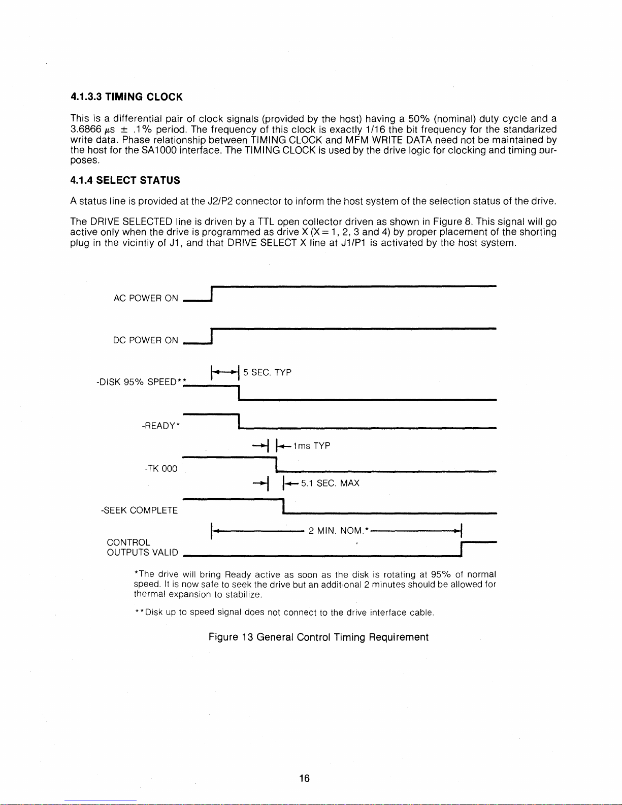
Since the SA1000 has a speed sense circuit'that prevents stepping until the disk is rotating at the proper
speed, no power
the disk
is
recalibrate itself
read/write functions can now begin. Refer to Figure
up
to
on
sequence
95%
of its normal rotational speed. At
to
TKOOO.
is
required. A
After a 18 msec head settle time,
READY
signal will be presented to the controller interface once
READY
time, after
SEEK
COMPLETE will go true. Normal seek and
an
initial power up, the drive will
3.
3.2 DRIVE SELECTION
Drive selection occurs when one of the Drive Select lines
will respond to the activated Drive Select line.
3.3 TRACK ACCESSING
Read/Write Head positioning
a.
Deactivating Write Gate.
b.
Activating the appropriate Drive Select Line.
c.
Being
in
the
READY
d.
Selecting the appropriate Direction.
e.
Pulsing the Step Line.
at
Stepping can occur
ed
at
the rate of incoming step pulses.
either the Normal or Buffered rate. During Normal Stepping, the heads are reposition-
at a high rate and are buffered into counters. When
is
accomplished
condition with
In
by:
SEEK
COMPLETE
the case of Buffered Stepping, incoming step pulses are received
all of the steps have been received, they are issued at a
ramped stepping rate, to the stepper drivers.
pulse will cause the heads to move either 1 track
Each
In
tion
result
line. A true
in
an
outward seek toward
on
the Direction
In
Line will cause
TKOOO.
in
an
3.4 HEAD SELECTION
is
activated. Only the disk appropriately jumpered
true.
or 1 track out, depending
inward seek; a false
on
the level of the Direc-
on
the Direction
In
Line will
Any of the 4 possible heads can
lines.
3.5 READ OPERATION
Reading data from the disk
a.
Deactivating the Write Gate Line.
b.
Activating the appropriate Drive Select Line.
c.
Assuring that the drive
d.
Selecting the appropriate head.
is
is
be
selected
accomplished
Ready.
by
placing that head's binary address
by:
7
on
the two Head Select

3.6 WRITE OPERATION
Writing data onto the disk
a.
Activating the appropriate Drive Select Line.
b.
Assuring that the Drive is Ready.
c.
Clearing any write fault conditions if they exist, by reselecting the drive.
d.
Selecting the proper head.
e.
Activating Write Gate and placing data
4.0 ELECTRICAL INTERFACE
The
interface of the
1.
Signal Interface
2.
DC
Power
3.
AC
Power
The
following sections provide the electrical definition for each line.
4.1
SIGNAL INTERFACE
The
signal interface consists of three categories:
is
accomplished
SA
1000 can be divided into three categories:
by:
on
the Write Data line.
1.
Control Input lines
2.
Control Output lines
3.
Data Transfer lines
in
All control lines are digital
disk controller (output)
via the interface connector J1/P1.
nature and either provide signals to the drive (input) or provide signals to the
The
they provide data and clocking, either to or from the drive,
NOTE: Refer to Figure
lines to carry
are uncommitted for the
not
be
SA
used as alternate signals if a controller having
3.
Those signal lines marked SPARE are uncommitted. They
1000 signals
SA1000, but are assigned for the
if
the user prefers to do his own modification. Those
data transfer signals are differential
via J2/P2.
may
be used as alternate
SASOO/SSO.
an
SA800/850 interface
Therefore, these signals should
signal
is
lines
used.
in
nature,
marked NA
8

DISK
CONTROLLER
FLAT RIBBON
OR
TWISTED PAIR
20
FT.
MAX
.,
TWISTED
PAJR
LOGIC
GROUND
FRAME GROUND
DISK CONTROLLER
--
-
-
-
-
-
-
--
-
-
--
-
-REDUCED WRITE CURRENT.,
SPARE
SPARE
-SEEK COMPLETE
NA
NA
-HEAD
SELECT
NA
-HEAD SELECT
-INDEX
-READY
NA
-DRIVE SELECT 1
-DRIVE SELECT 2
-DRIVE SELECT 3
-DRIVE SELECT 4
-DIRECTION
-STEP
NA
WRITE
GATE
-TRACK 000
-WRITE FAULT
NA
NA
NA
+5V
DC
-5VDC (-7V
to
-16VDC OPT)
+ 24V
DC
ACINPUT
FRAME GROUND
ACINPUT
1
..
2
4
6
8
10
12
2°
21
IN
...
-
...
~
..
~
...
--
..
.~
~
--
~
-
-
-
14
16
18
20
22
24
26
28
30
32
34
36
38
40
42
44
46
48
5
4
1
1
2
3
50
AC
5
7
9
11
13
15
17
19
21
23
25
27
29
31
33
35
37
39
41
43
45
47
49
6
3
2
MOTOR GROUND
~
-
DRIVE
LOGIC GROUND
~51P5
-
SINGLE
SA1000 DRIVE
J1/P1
WIRE
STRAP
J4/P4
Figure 3
J1
Interface and Power Connection
9

4.1.1 CONTROL INPUT LINES
The control input signals are of two types: those intended to be mutliplexed
those intended to control the multiplexing. The control input signals to be mutliplexed are
IN,
HEAD SELECT 20 and
do the multiplexing
is
DRIVE
21,
WRITE
SELECT
GATE
and REDUCED WRITE CURRENT. The signal which
1,
DRIVE
SELECT
2,
DRIVE SELECT
in
a multiple drive system and
STEP,
DIRECTION
is
intended to
3,
DRIVE SELECT
4.
The input lines have the following electrical specifications. Refer to Figure 4 for the recommended circuit.
+5
V
20ft (MAX.)
330n
Figure 4 Control Input Driver/Receiver Combination
The 7438 has the following characteristics:
=
True
O.OVDC
False = 2.5VDC to 5.25 VDC @ lin = 250
Only 1 drive
drives. A
to
O.4VDC
in
the system should be terminated, if floppy disks are daisy chained together with SA1000
SA
1000 should be physically located at the end
@ lin = 40 ma(max)
Ita
(open)
of
the cable and terminated at
IC
location
BC.
A 220/3300 resistor pack, located at
IC
location
4.1.1.1 DRIVE SELECT 1·4
DRIVE
SELECT,
when logically true, connects the drive to the control lines. Only one DRIVE SELECT line
may be active at a time.
Jumper options
DS1,
DS2, DS3, and
DS4
are used to select which drive select line will activate the interface
for that unique drive.
4.1.1.2 DIRECTION IN
This signal defines the direction
of
motion of the read/write heads when the
cuit or logical false, defines the direction as
head will move away from
is
of motion
defined as
the
center
of
the disk. If the input is shorted to ground, or logical true, the direction
"in"
and if a pulse is applied to the
the center of the disk.
"out"
8C,
provides input line termination.
and if a pulse
STEP
is
applied to the
line, the read/write heads will move towards
STEP
line is pulsed.
STEP
line, the read/write
An
open cir-
10

4.1.1.3 STEP
This line causes the read/write heads to move
tion is initiated at each
least
200 ns before the trailing edge of the step pulse. Stepping can be performed
Buffered mode:
-DIRECTION
logical true to false transition. Any change
~
W!!/f!!fIl/f!lI~~~rm
~-------~~~~------------------~SS~--------
J
-STEP
l
------.U
--1
-SEEK
COMPLETE
Figure 5 Normal Step Mode
• Normal Step Modepulses. The minimum time between successive steps
3.0j.ts.
Refer to Figure
• Buffered Step Modecounter. After the last step pulse, the read/write heads will begin stepping the desired number of
cylinders and
tle
on
the cylinder. This mode
pulses is the less than
In
this mode, the read/write heads will move at the rate of the incoming step
5.
In
this mode, the step pulses are received at a high rate and buffered into a
SEEK
COMPLETE (Refer to Section 4.1.2.5) will go true after the read/write heads set-
of
operation is
200j.tsec.
~
200ns MIN.
I
t-3.0I's
j.----1.5ms
~
500ns
I
in
the direction
MIN. I
TYP
automatically
as
defined by the DIRECTION
in
the DIRECTION
MIN.~
.....
_-\~""'~
IN
line must be made at
in
either the Normal or
____
U
18ms
TYP
~
is
1 .5ms, with a minimum pulse width of
selected
when the time between step
~
Sr-,~_
IN
line. The mo-
_
100 ns after the last step pulse has been sent to the drive, the DRIVE SELECT line may be dropped
and a different drive selected.
The maximum time between steps is
6).
NOTE: A high pitched noise may be present if
data cable disconnected (no timing clock signal). It's the stepper motor trying to return to track
zero with
avoided.
no
step pulses present. While this will not damage the drive, this condition should be
-----.-,
DIRECTION
-
-
STEP
--1
-
SEEK
COMPLETE
-
DRIVE
SELECT
X
----------------------------~
200j.ts
with a minimum pulse width of
AC
and
-~~~~~~~
~
500ns
TYP
I
Figure 6 Buffered
DC
power are applied to
...,
~
200ns MIN.
I
~----~s~----------
J.-150ms
I
-..t
~200ns
J
Step Mode
3.0j.ts.
(Refer to Figure
an
SA
1000 with the
MAX.
~
SS
MIN"
SS~----
I
NOTES:
1.
Step pulses with periods between
guaranteed if this timing requirement is violated. ,
2.
A 220/3300 resistor pack,located at
200j.ts
and 1.5ms are not permitted. Seek accuracy is not
IC
location
11
8C,
allows for Step line termination.

4.1.1.4 HEAD SELECT 2° and
21
These two lines
HEAD
SELECT
Table 1 shows the HEAD
rrovide
for the selection of each individual read/write head
2 is the least significant line. When all HEAD
SELECT
Figure 7 for the timing sequences).
A
220/330n resistor pack, located at
HEAD
SELECT
2°
1
1 0
0 1
0 0
LINE
21
1
Table 1 Head Select
4.1.1.5
The active state of this
tive state of this
WRITE GATE
signal (logical zero level) enables
Signal (logical one level) enables data to
pulses to reposition the head arm.
in
a binary coded sequence.
SELECT
lines are false, head 0 will be selected.
SEQUENCE and model variations for the HEAD
IC
location
8C,
HEAD#
SA1002
allows for input line termination.
SELECTED
0 0
1 1
-
-
(1
= False, 0 = True)
WRITE
DATA to
be
transferred from the drive and enables
HEAD#
SA1004
be
written onto the disk. The inac-
SELECT
SELECTED
2
3
lines. (Refer to
STEP
HEADS SWITCHED
READ DATA
VALID
~:~~~~::E
~:8~
CONTROLLER)
-.j
~
20l's
MAX.
~
____
~I
---+----------~
----~I----------
.......
~
460ns
,--,L..
Figure 7 Head Selection Timing
220/330n resistor pack, located at
A
IC
location
8C,
allows for termination of this line.
4.1.1.6 REDUCED WRITE CURRENT
When this interface
128 through 255). When this
signal
is
low (true) the lower value of Write Current is selected (for writing on cylinders
Signal is high (false), the higher value of Write Current
cylinders 0 through 127). A 220/330n resistor pack, located at
I
~
~201'S
MAX.
t7Ax
________
Ie
location
__
8C,
allows for line termination.
is
selected (for writing
on
12

4.1.2 CONTROL OUTPUT LINES
The control output signals are driven with
40 ma at
logical zero (true), with a maximum voltage of
at logical one (false) the driver transistor
an
open collector output stage capable of sinking a maximum of
is
off and the collector cut off current
OAV
measured
at
the driver. When the line driver
is
a maximum of 250
microamperes.
All
J1
output lines are enabled by their respective
DRIVE
SELECT
line.
Figure 8 shows the recommended control signal driver/receiver combination.
+5
V
20ft (MAX.)
330n
Figure 8 Control Output Driver/Receiver Combination
4.1.2.1 TRACK 000
This interface signal indicates a true state (logical zero) only when the selected drive's read/write heads are
is
at track zero (the outermost data track) and the access circuitry
stepper motor.
This)signal
is
false (logical
one)
when the selected drive's read/write head
driving current through phase one of the
is
not at track zero.
is
4.1.2.2 INDEX
The
drive provides this interface signal once each revolution (19.2ms) to indicate the beginning of the track.
Normally, this signal is a logical one and makes the transition to logical zero for a period of approximately
OILS
once each revolution. Refer to Figure
1
INDEX
~
1
..
9.
________________ r-1 ___ __
~10I"STYP
19.2ms NOM. •
I
Figure 9 Index Timing
4.1.2.3 READY
This interface signal when true (logical zero), together with
ready to read, write, or seek and that the signals are valid. When this line
is
the disk and seeking
will
be
Ready
power
on
true after the drive
is
5 seconds.
inhibited at the drive.
is
95 ± 2%
up
to speed. The typical time for READY to become true after
SEEK
COMPLETE,
is
false (logical one), all writing to
indicates that the drive
is
13

4.1.2.4 WRITE FAULT
This signal when active (logical zero) is used to indicate that a condition exists
improper writing
•
WRITE
on
the disk. A
CURRENT
WRITE
in
the head without
FAULT occurs whenever one of two conditions occur:
WRITE
GATE
active.
at
the drive that could cause
• Multiple heads selected.
To
reset the
WRITE
FAULT line, deselect the drive for at least 500
ns.
4.1.2.5 SEEK COMPLETE
SEEK
COMPLETE will
completion of a seek. Reading or writing should not be attempted until
• A recalibration sequence
go
true (logical zero) when the read/write heads have settled
SEEK
SEEK
COMPLETE will go false
is
initiated (by the drive logic) at power
in
two cases:
on
if the read/write heads are not
on
COMPLETE
over track zero.
• 500
NS
typical, after the leading edge of a
STEP
pulse (or the first of a series of step pulses).
4.1.3 DATA TRANSFER LINES
lines associated with the transfer of data between the drive and the host are differential
All
may not
and TIMING CLOCK and are provided at the J2/P2 connectors
driver/receiver combination.
be
multiplexed. These three pairs of balanced signals are: MFM
WRITE
on
all drives. Figure 10 illustrates the
DATA,
the final track at the
is
true.
in
nature and
MFM
READ
DATA,
HIGH
TRUE
Figure
FLAT CABLE
r*-_....;;.20;;.;.;ft~M;;..;;AX...;;...
10
Data Transfer Line Driver/Receiver Combination
+SIGNAL
-SIGNAL
_.
_,""*,
5Hl
x 2
>-_
75107B
HIGH
TRUE
14

HOST
FLAT CABLE
OR TWISTED
PAIR
20
FT
MAX
..
--
..
.:
-
-DRIVE
GND
SPARE
GND
SPARE
GND
SPARE
GND
+
TIMING
-TIMING
GND
GND
+
MFM
-MFM
GND
GND
+
MFM
-MFM
GND
GND
SELECTED
ClK
ClK
WRITE DATA
WRITE DATA
READ DATA
READ DATA
..
-
~
-
..
-
..
~
1
:3
5
7
9
10
13
14
17
18
11
12
15
16
19
20
2
DRIVE
4
J2/P2
6
8
-==
-
Figure
11
J2
Interface
Connection
-==-
-
4.1.3.1 MFM WRITE DATA
This pair of signals ,defines the transitions (bits) to be written on the disk. + MFM WRITE DATA going more
positive than -MFM
WRITE GATE is active. This signal must be driven to an inactive state
than -MFM
WRITE DATA.
WRITE DATA) by the host system when in the read mode. Figure 12 shows the timing for MFM
WRITE DATA will cause a flux reversal on the track under the selected head providing
(+
MFM
WRITE DATA
more
negative
4.1.3.2 MFM READ DATA
The data recovered by reading a pre-recorded
of MFM READ DATA lines. This transition of the
READ
DATA line represents a flux reversal on the track of the selected head while WRITE GATE is inactive.
to
Refer
Figure 12.
-
DRIVE
SELECT
track
is transmitted to the host system via the differential pair
+ MFM READ DATA line going more positive than -MFM
~~---------------------------------
-HEADSELEGT
+
MFM
VALID
READ
DATA
20ILs
---,~
MAX.
____________________________________________
--1
~,
-.j
~ 50ns
TYP
__
-WRITE
+MFM
WRITE
GATE
DATA
--------------------------~~----------------
----~I·-------2-0-IL-S-M-A-X·------·~1
!
I I
460ns
MAX·
.... I
~
--.j
~
BIT
CELL
= 230ns
Figure 12 MFM Read/Write Data Timing
TYP
-..J
j.-
15
-1
Pj-----------------
50~S
MIN. to 150ns
MAX.
4.1.3.3 TIMING CLOCK
This is a differential pair of clock signals (provided by the host) having a
3.6866
write data.
the host for the
poses.
4.1.4 SELECT STATUS
A status line
The
active
plug
p,s ± .1
DRIVE
only when the drive
in
the vicintiy of
-DISK
% period.
Phase relationship between TIMING CLOCK and MFM
SA1
000 interface. The TIMING CLOCK
is
provided at the J2/P2 connector to inform the host system of the selection status of the drive.
SELECTED
AC POWER ON
DC
POWER ON
95%
SPEED*_*
The
frequency of this clock
line
is
driven by a
is
programmed
J1,
and that DRIVE
---1
---.J
H5SEC.
___
--.
is
is
TTL
open collector driven
as
drive X
SELECT
TYP
(X
= 1 ,
X line at
exactly 1/16 the bit frequency for the standarized
WRITE
used by the drive logic for clocking and timing pur-
as
shown
2,
3 and
4)
by proper placement of the shorting
J1/P1
is activated by the host system.
50% (nominal) duty cycle and a
DATA need not be maintained by
in
Figure
8.
This signal will go
-READY*
-...J
~1ms
-TKOOO
-----
....
1
~.
___________________________
--..J
COMPLETE
-SEEK
I
.....
.....--------2 MIN. NOM. *
CONTROL
OUTPUTS VALID •
*The drive will bring Ready
speed.
thermal expansion to stabilize.
* * Disk up to speed signal does not connect to the drive interface cable.
_______________________________________
active
It is now safe to seek the drive but an additional 2
Figure 13 General Control Timing Requirement
TYP
I~
5.1
SEC.
MAX
-------i~~1
as soon as the disk is rotating at
minutes
should be allowed for
~I~
95%
__
----
of normal
16

4.1.5 GENERAL TIMING REQUIREMENTS
The timing diagram
restrictions) for proper operation of the drive.
Note that a
recal sequence to function, the following conditions must be met:
• TIMING CLOCK
•
• Spindle
POWER INTERFACE
4.2
The
SA
DC
power is used for the electronics and the stepper motor.
4.2.1 AC
The
AC
AC
power requirements.
4.2.2 DC
DC
power to the
and their specifications along with their J5/P5 pin designations, are outlined
recalibrate to track zero sequence
STEP
Input at
will not occur until disk
tion
1000 requires both
POWER
power
POWER
as
shown
is
J1/P1
is
spinning at regular speed (if
is
via the connector J4 mounted at the center rear of the drive. Table 2 shows a listing of the
_drive
is
in
Figure 13 shows the necessary sequence of events (with associated timing
is
initiated automatically at every
supplied to the drive (via J2/P2).
is held inactive.
AC
and
DC
is
up to speed).
AC
and
DC
power for operation. The
via connector J5/P5 located
on
are switched
AC
the solder side of the
on
power
at the same time, stepping ac-
is
used for the drive motor and the
PCB.
in
DC
power
Table
on.
The three
3.
For this auto-
DC
voltages
NOTE: The
with a ground strap
tion of these grounds, remove the strap.
SA
1
abo
is
shipped with
located
DC
(base casting) and
on
the drive motor. If the system configuration requires the separa-
AC
ground (drive motor) connected together
17

60HZ
50HZ
CONN
MAX
INRUSH
CURRENT
MAX
RUN
FREO
TOl
P4
1
2
3
(3
SEC)
CURRENT
110V
(STANDARD)
90-127V 180-253V
FRAME
90-127V RTN 180-253V
2.6A
1.0A
GND
± 0.5
203/230V
FRAME
1.1/1.25A
0.5A
HZ
Table 2 AC Power Requirements
GND
110V
90-127V
FRAME
90-127V
RETURN
2.6A 1.2A
1.1A 0.6A
GND
± 0.5
180-253V
FRAME
180-253V
-
HZ
220V
GND
P5
CONNECTOR
+24
± 2.4V
P-P
1V.
MAX.
Ripple
+5
± O.25V
P-P
50mV
MAX. Ripple
(-7
TO -16V OPT)
-5 ± O.25V
50mV
P-P
MAX. Ripple
STEAD Y STATE
MAX.
TYP
O.25A O.20A
4.1A
O.25A
Table
3 DC Requirements
3.6A 2.5A
O.20A O.25A
CURRENT
STEPPING
MAX. TYP
3.3A 2.8A
2.0A
O.20A
-
18
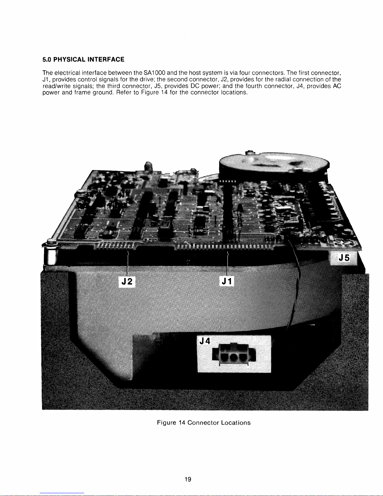
5.0 PHYSICAL INTERFACE
The electrical interface between the
J1,
provides control signals for the drive; the second connector,
read/write
signals; the third connector,
power and frame ground. Refer to Figure
SA
1000 and the host system
J5,
provides
14
for the connector locations.
DC
is
via four connectors. The first connector,
J2,
provides for the radial connection of the
power; and the fourth connector,
J4,
provides
AC
Figure
14
Connector
19
Locations
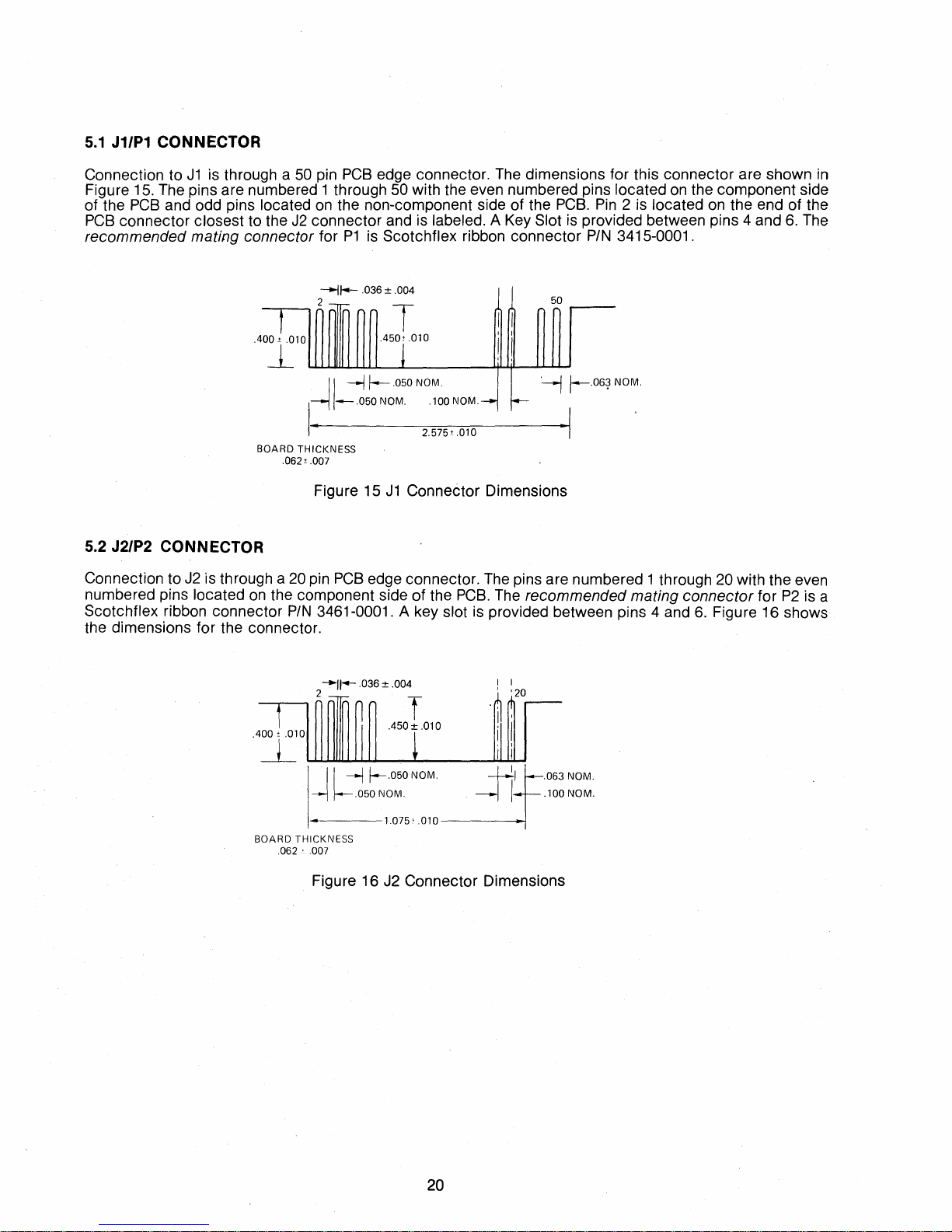
5.1
J1/P1 CONNECTOR
Connection to
Figure
of the
PCB
recommended mating connector for
15.
PCB
connector closest to the
J1
The pins are numbered 1 through
is through a
and odd pins located
50
J2
t
.4 00 ± .010
pin
on
connector and
-.j~
2-r-
~
--11
I·
BOARD
THICKNESS
.062± .007
Figure 15
5.2 J2/P2 CONNECTOR
Connection to
numbered pins
Scotchflex ribbon connector
the dimensions for the connector.
J2
is through a
located
20
pin
on
the component side
PIN
3461-0001. A key slot
PCB
edge connector.
50
the non-component side of the
P1
.036 ± .004
with the even numbered pins located
is
labeled. A Key Slot
is
Scotchflex ribbon connector
T
.450r
.010
--j
f--.050 NOM.
-.050
NOM.
PCB
edge connector.
.100NOM.-
2.575± .010
J1
Connector Dimensions
of
the
The
dimensions for this connector are shown
I
I
I
I
,
,
~
The
pins are numbered 1 through
PCB.
The
recommended mating connector for
is
provided between pins 4 and
on
PCB.
Pin 2 is
is
provided between pins 4 and
PIN
3415-0001.
50
'--j
NOM.
f-.06~
the component side
located
-I
on
the end of the
20
with the even
P2
6.
Figure 16 shows
6.
in
The
is a
--r
t
400,
~
BOARD
.062
2
--.,,--
.036 ± .004 !
----
.010
-r-
1
T
.450±
.~
.010
·1
:',
I
.,
I --j
f---'O~ON.
---1
f---.050
-
THICKNESS
..
007
Figure 16 J2 Connector Dimensions
OM.~.II
NOM. . --I I .100 NOM.
1.075'
.010
20
I
!
~
.063 NOM.
20
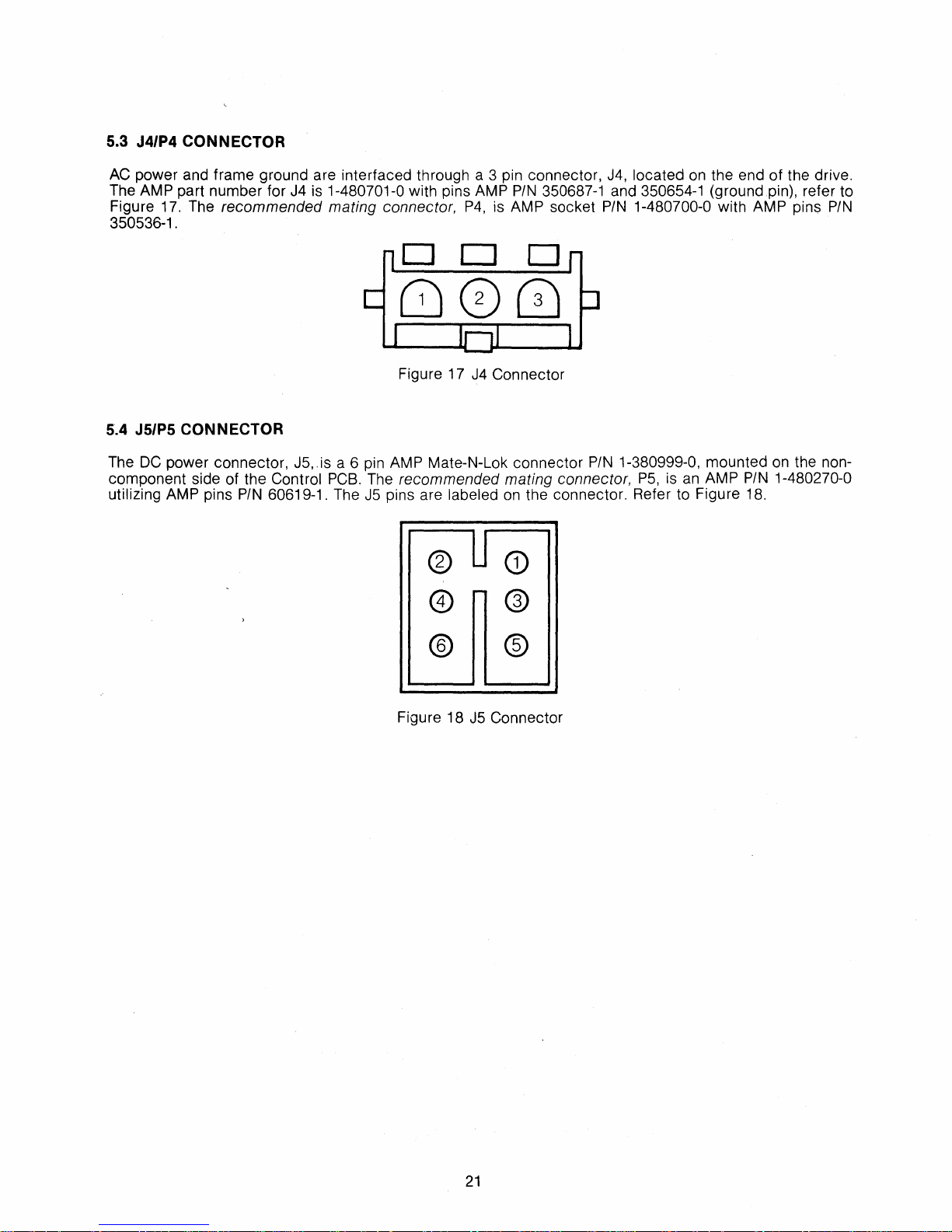
5.3 J4/P4 CON N ECTOR
AC
power and frame ground are interfaced through a 3 pin connector,
J4
is
The AMP part number for
17.
Figure
350536-1.
The recommended mating connector,
1-480701-0 with pins AMP
P4,
PIN
is AMP socket
J4,
located
350687-1 and 350654-1 (ground pin), refer to
PIN
1-480700-0 with AMP pins
on
the end of the drive.
PIN
5.4 J5/P5 CONNECTOR
The
DC
power connector, J5,.is a 6 pin AMP Mate-N-Lok connector
component side of the
utilizing
AMP pins
Control
PIN
60619-1. The
PCB.
Figure 17
The
recommended mating connector,
J5
pins are labeled
Figure 18
®
@
®
J4
Connector
on
CD
-
@
®
J5
Connector
the connector. Refer to Figure
PIN
1-380999-0, mounted
P5,
is
an
AMP
on
PIN
1-480270-0
18.
the non-
21
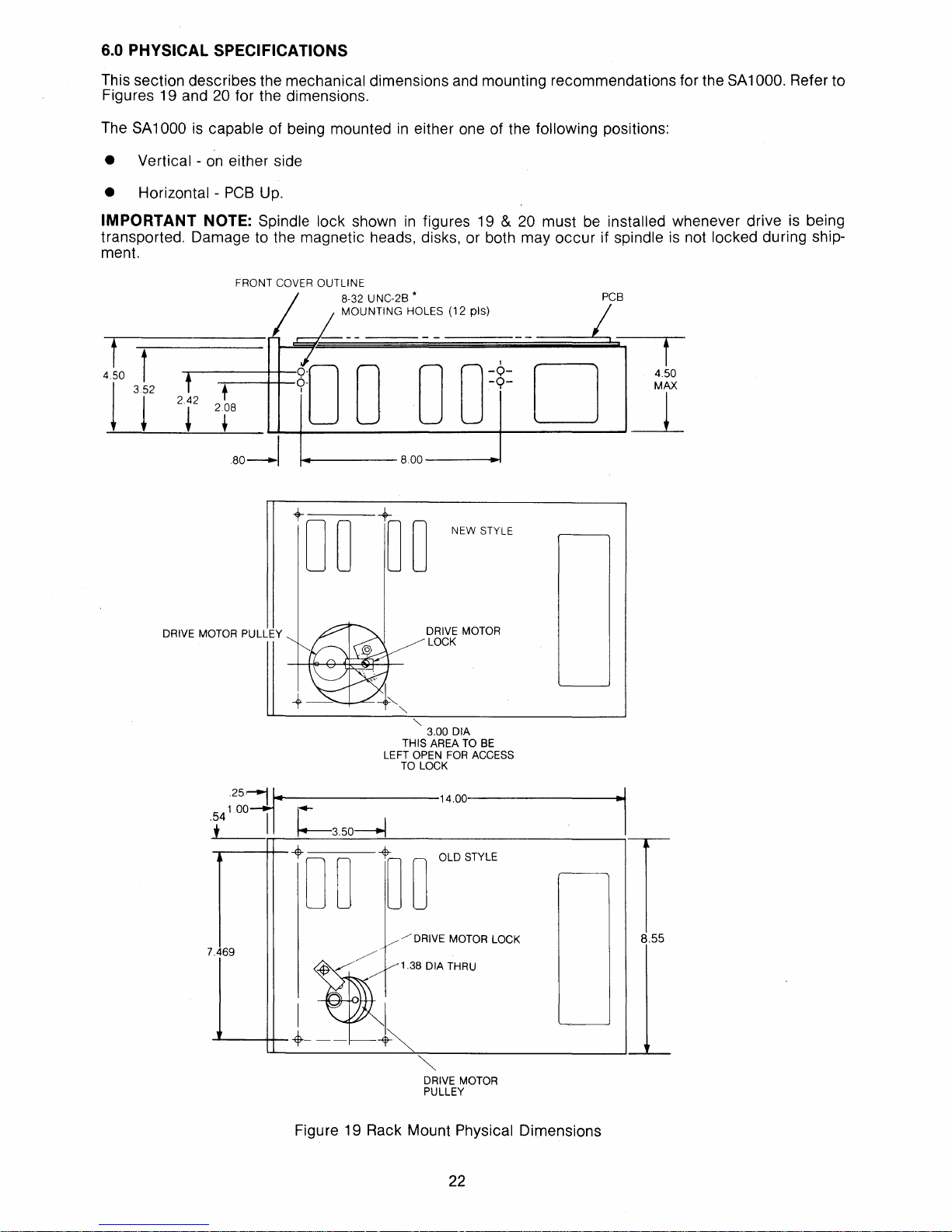
6.0 PHYSICAL SPECIFICATIONS
This section describes the mechanical dimensions and mounting recommendations for the
Figures 19 and
The
SA
1000
• Vertical -
• Horizontal -
IMPORTANT NOTE: Spindle lock shown
transported. Damage to the magnetic heads, disks, or both may occur if
ment.
1r
iT
20
for the dimensions.
is
capable of being mounted
on
either side
PCB
Up.
FRONT COVER OUTLINE
J-
0-
t
2.42
+
t
208
t
80~1
I
'0
in
either one of the following positions:
in
figures
8-32 U NC-2B
~~UNTING
0
..
HOLES
0
8.00
19 & 20
(12
pis)
0
-9-
0-
NEW STYLE
must
-
-
D
be
installed whenever drive
spindle
PCB
is
not locked during ship-
I
f
4.50
MAX
~
SA1
000. Refer to
is
being
DRIVE MOTOR PULLEY
.25~14"
.• 4 100
7.469
-II
....... ' --++-<t-
DRIVE MOTOR
LOCK
"-
3.00 DIA
THIS
AREA
TO
BE
FOR
ACCESS
OLD STYLE
THRU
___
-----14.00
~3
50----+\
/.
I
~~'38
LEFT OPEN
TO
LOCK
DIA
-~-~~
~
DRIVE MOTOR
PULLEY
T
8.55
Figure 19 Rack Mount Physical Dimensions
22

FRONT COVER OUTLINE
8-32 U NC-2B *
MOUNTING HOLES
.....
-----
....
--------1~.aa--------I~
8.0.0.
-----+I
(20
NEW
pis)
PCB
STYLE
,DRIVE MOTOR PULLEY
,.251
....
1.0.0.
.~4 I ~3
9l_
DRIVE MOTOR
LOCK
"'-
3.0.0.
AREA
THIS
LEFT
OPEN
TO
SPINDLE
4--------14.0.0.
I"
5Q.---.t
//DRIVE
~l~
DIATHRU
t
~
DRIVE MOTOR
PULLEY
DIA
TO
BE
FOR
ACCESS
LOCK
OLD
STYLE
MOTOR LOCK.
T
9.14
Figure 20 Standard Mount Physical Dimensions
23

7.0 MEDIA DEFECT & ERRORS
Introduction
In
high density digital recording storage systems it is necessary to increase the reliability or improve the
operational performance
the predominant error pattern
sent bits) or shifted bits from their
These errors are due
ror occurrence. The error rate
cuits, head and pOSitioning of actuator.
by
providing
to defects
an
error detection and correction scheme. For disk storage systems,
is
a burst of errors occurring
nominal position more than the data separator can tolerate them to shift.
in
the media
is
dependent upon noise and phase characterisitics of media, Read/Write cir-
as
well
as
in
one or more tracks which are drop outs (ab-
signal to noise ratio contributing to probability of er-
What Is The Definition Of
An
error
is
any discrepancy between recovered data and true correct recorded data. There can be
bit or a missing bit, i.e., a
cari be
system.
If
classified into soft or hard errors. Soft errors are generally related to signal to noise ratio of the
an
error
is
repeatable with a high probability, it
An
"zero"
Error?
can be transformed into
is
due to media defect ahd
"one"
or a
"one"can
How Will Shugart Find the Errors?
The errors will be identified prior to shipment and information incorporated
user to skip those defective
which exercises the drive
of each bit recorded
on
locations per his system capability. Shugart has a unique media test system
in
extreme marginal conditions and measures the amplitude and phase distortion
the disk storage.
Error Reporting
A map will
cylinder and head address. Additionally, cylinder 000
be
provided with each drive showing defective bytes as a location from index identified by
is
guaranteed to
be
Error Acceptance Criteria
There will be no more than
defects.
ple
single defect is defined
A
than 2 bytes
long, or a single error
12
tracks with defects per head of which no more than 4 tracks will contain mUlti-
as
an
error less than 2 bytes long. A multiple defect is defined
in
several sectors.
an
be
changed to"zero".Errors
is
termed a hard error.
in
a usable format to enable the
error free.
as
an
error greater
extra
24

8.0 SA1000 TRACK FORMAT
The
purpose of a format is to organize a data track into smaller, sequentially numbered, blocks of data called
sectors. The
by
a prewritten identification (1.0.) field ·which contains the physical sector address, plus cylinder and head
information. The
The
soft sectored format is a slightly modified version of the I.B.M. system 34 double density, which
monly used on 8 inch floppy disk drives. The encoding method used here
SA
1000 format is a soft sectored type which means that the beginning of each sector is defined
1.0. field is then followed by a user data field.
is
modified frequency modulation
(MFM).
In
the example shown (Figure
in
bytes
The
length.
beginnings of both the I.D. field and the data field are flagged by unique characters called address
21),
each track is divided into
32
sectors. Each sector has a data field of 256
marks.
An
address mark is 2 bytes
an
"FE"
pattern which
in
length. The first byte is always
is
the pattern used to define
an
"A1"
data pattern. This is followed by either
an
1.0. address mark, or
an
"F8"
which is a data ad-
dress mark pattern.
The
"A1"
pattern is made unique by violating the encode rules of MFM by omitting one clock bit. This makes
the address mark pattern unique to any other serial bit combination.
Each
1.0. and data field are followed by a 16 bit cyclic redundancy check (CRC) character used for data
verification. Each
CRC polynomial is unique for a particular data pattern.
is
com-
Surrounding
8.1
GAP LENGTH CALCULATIONS
8.1.1
GAP 1
The
1.0. and data field are gaps called Interrecord gaps.
Gap 1 's purpose is to provide a head switching recovery period so that when switching from one track to
another, sequential sectors may
11
bytes long which corresponds to the head switching time of 20 microseconds1 Gap 1
followed by a sync field for the
be
read without waiting the rotational latency time. Gap 1 should
1.0. field of the first sector.
be
at least
is
immediately
8.1.2 GAP 2
Following the 1.0. field, and separating the 1.0. field from the data field,
area for the data field write update splice to occur.
The
for the data field address mark.
length of gap 2 is determined by the data separator lock up perfor-
The
remainder of this gap also serves as the sync up area
is
gap
2.
Gap 2 provides a known
mance.
8.1.3 GAP 3
Gap
3,
following the data field, is a speed variation tolerance area. This allows for a situation where a track
has been formatted while the disk
ing
3% faster than nominal (power line variations).
Gap 3 should
be
at least 15 bytes
is
running 3% slower than nominal, then write updated with the disk runn-
in
length.
8.1.4 GAP 4
Gap 4 is a speed tolerance buffer for the entire track. This allows the disk to rotate at least 3% faster than
normal without overflowing the track during the format operation. The format operation which writes the
1.0.
fields, begins with the first encountered index and continues to the next index.
25

8.2 WRITE PRECOMPENSATION
Whenever two bits are written
curs, which tends to cause the two bits to move away from each other. This
Other phenomenon such
degree.
The
effect of bit shift can
will occur early and which bits will occur late, can
the expected shift.
Bit shift is more apparent
should only be at track number greater than 128.
The
optimum amount of pre-compensation for the
bits.
TABLE
4 shows various bit patterns for pre-compensation.
in
close proximity to each other, a phenomenon called pulse superposition oc-
as
random noise, speed variation, etc., will also cause bit shift, but to a lesser
be
reduced by a technique called precompensation which, by detecting which bits
be
done by writing these bits
on
the innermost data tracks due to pulse crowding. Therefore, precompensation
SA
1000
is
12
nanoseconds for both early and late written
WRITE
POSITION
o 0
0 0
o 0
o 0 1
0
1
0
o 0 1 1
o 1
o 0
DIRECTION
On
Time Clock
Late Clock
=
On
Time Data
Early Data
OF
SHIFT
o 1 o 1
o 1 1 0
o 1
1 1
100
1 o 0 1
1 0 1
1
o 1
o 0
1 1
1 1 o 1
1
1 1
1
1 1 1
0
0
1
0
= Late Data
=
On
Time Data
Early Clock
=
On
Time Clock
On
Time Data
Early Data
=
= Late Data
=
On
Time Data
is
a large factor of bit shift.
in
the opposite direction of
Table
4.
Write Precompensation
Precompensation Pattern Detection bits are shifted through a 4 bit shift register. Bit
third position.
INDEX~------------------------------~ll~-------------------------------------------
GAP
WRITE
UPDATE
-------------------------'
16
1 SYNC
x '4E'
ID.A.M.
----
NOTES:
1,
NOMINAL
2.
MINIMUM
3.
WRITE
4.
HEAD SWITCHING TIME = 20 MICROSECONDS.
TRACK CAPACITY - 10416 BYTES.
TRACK CAPACITY -
TO
READ RECOVERY TIME = 20 MICROSECONDS.
Figure
DATA
A.M.
----
(NOMINA~
21
Track Format
DATA
FIELD
256 x USER
-
3%
SPEED VARIANCE) 10102 BYTES.
DATA
is
written out of the
GAP
3
15
x '4E' 352 x '4E'
GAP
nL
4
26

9.0
SA1000 JUMPER OPTIONS
The
following jumper options are located
tions.
on
the control
PCB,
PIN
26050. Reference Figure 15 for the loca-
JUMPER
Fault When jumpered, this option disables the fault detection circuitry.
Ready When jumpered, this option
Drive
Select When jumpered, this option selects the designated drive.
(081 -
-5,
4)
-15
Volts When jumpered
FUNCTION
in
the
be used when the input
figuration, this option
,~~~~
••
~~
®
allows a -15 volt input to
FAULT
enables
~5
volt configuration, this option bypasses the regulator chip - to
voltage is rated at
an
active ready signal at the interface.
-5
volts
..
When jumpered in the -15 volt con-
be
regulated to
-5
READY
volts.
J
-5,
- 15
VOLTS
JUMPER
Figure 22 SA1000 Control PCB
27

10.0 SA1000 UNPACKAGING INSTRUCTIONS
Attention: These instructions must
1.
The
spindle lock (PIN 60464) must
2.
the figure
To
prevent possible damage to the heads and media, rotate the spindle
below). Retain the lock for reinstallation prior to transporting the drive.
only.
3.
To
isolate the
AC
ground from logic ground, remove the motor ground strap (PIN 60060).
be
carefully followed to insure the proper operation of the drive.
be
removed before applying
AC
power
to
the drive (reference
in
a clockwise direction
Figure 23
SA
1000 Packaging
28

 Loading...