

AT-501
Cortex-A5
System on Module
Integration guide
Revision 1.4

Contents
1 Scope ..................................................................................................................................................... 4
1.1 SoM introduction ............................................................................................................................. 4
1.2 SoM models ..................................................................................................................................... 4
2 AT-501 Integration guide ...................................................................................................................... 6
2.1 Power connectivity .......................................................................................................................... 6
2.2 Reset ................................................................................................................................................ 8
2.3 Interfaces ......................................................................................................................................... 9
2.3.1 Ethernet ports ......................................................................................................................... 9
2.3.2 UART and USART ................................................................................................................... 10
2.3.3 USB ........................................................................................................................................ 12
2.3.4 High Speed Multi-Card Interface ........................................................................................... 14
2.3.5 LCD and touch screen support .............................................................................................. 14
2.3.6 CAN ........................................................................................................................................ 16
2.3.7 I2C .......................................................................................................................................... 16
2.3.8 SPI .......................................................................................................................................... 16
2.3.9 A to D Convertor ................................................................................................................... 16
2.3.10 JTAG .................................................................................................................................. 17
2.4 Mechanical considerations ............................................................................................................ 17
2.4.1 SO-DIMM connector ............................................................................................................. 19
2.5 Pin assignment ............................................................................................................................... 19
2.5.1 SO-DIMM 200 Pins assignment ............................................................................................. 19
2.5.2 Port A options........................................................................................................................ 26
2.5.3 Port B options ........................................................................................................................ 27
2.5.4 Port C options ........................................................................................................................ 28
2.5.5 Port D options ....................................................................................................................... 29
2.5.6 Port E options ........................................................................................................................ 30
3 AT-501 System overview ..................................................................................................................... 31
3.1 Cortex-A5 Processor ...................................................................................................................... 31
3.2 Memories ....................................................................................................................................... 31
2 | AT-501 HW user manual 1.4

Revision
Date
Description
1.0
12.6.2013
Initial version
1.1
8.5.2014
Add D36, update USART capabilities.
1.2
1.6.2014
Add notes about OTG support; add details
about components height on the print side.
1.3
6.4.2015
Fix debug port pin out
1.4
26.8.2015
Add remarks about VBAT and Resistive touch
interfaces
Document Revision History
3 | AT-501 HW user manual 1.4

1 Scope
The purpose of this document is to provide a guide for integrating the AT-501 into the target hardware
in an easy and fast way so that the use of SoM will shorten and simplify the development process.
The guide is divided to two parts, the first one help you through the integration process, giving design
samples based on the design of the CB-20(schematics can be provided by Shiratech via
support@shiratech.com ) while the second part provide more details on the AT-501 system.
In order to simplify the integration process we recommend the following process:
1. Read through the integration guide on the required interfaces.
2. Use Shiratech’s Pin configuration tool to define the solution
3. Use the CB-20 as a reference design to shorten the development process.
For more details if needed review the SAMA5D3 user manual and access Shiratech at
support@shiratech.com
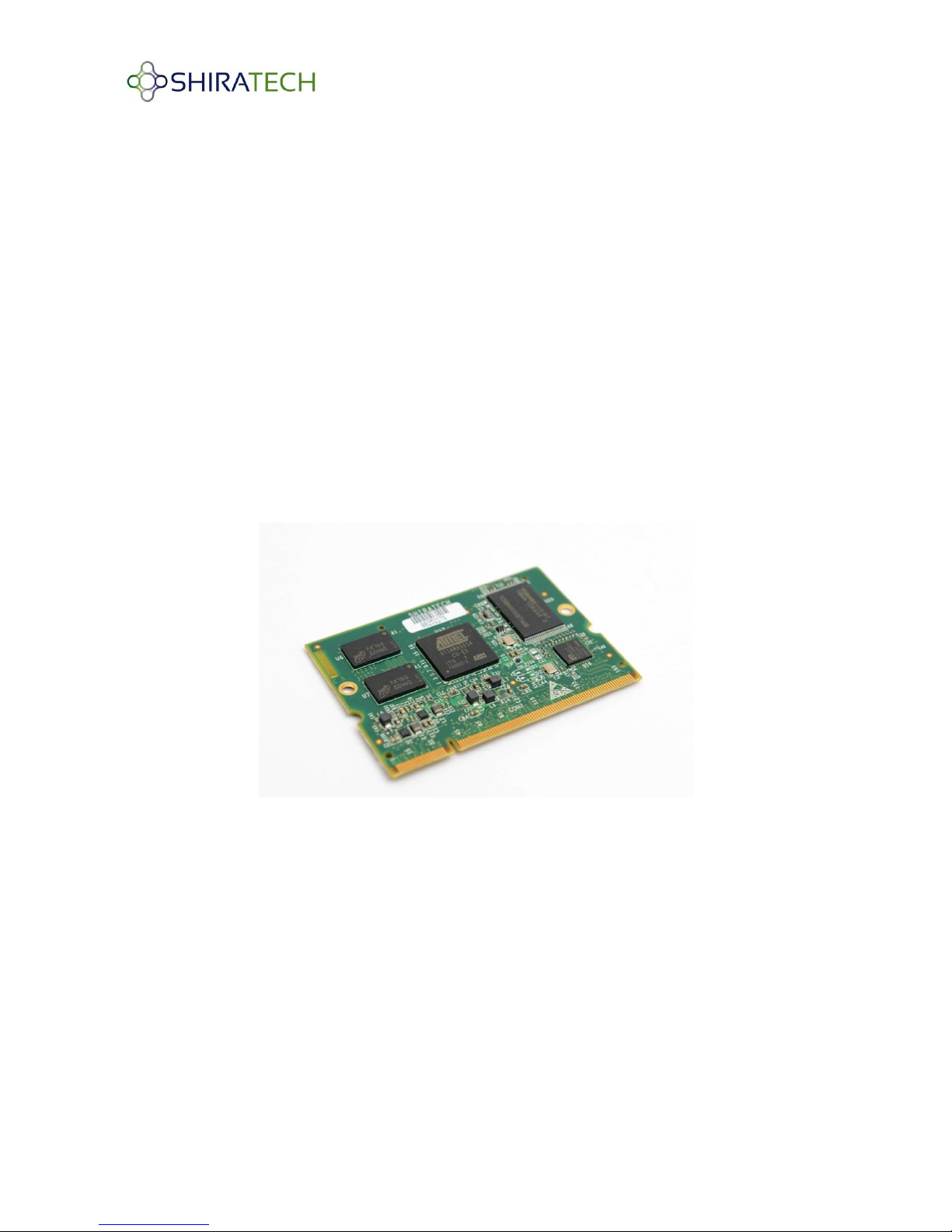
1.1 SoM introduction
The AT-501 is an industrial embedded System-On-Module (SoM) based on Atmel’s new SAMA5D3
Cortex-A5 system on chip. It offers the optimal balance of the most power efficient Cortex A processor
available to date with a high performance CPU running at 536 MHz and a floating point unit.
The AT-501 includes the processor and its entire environment, as well a 1Gbe physical layer chip. All the
interfaces of the processor are available for the user through a well-known 200 pins SO-DIMM form
factor.
1.2 SoM models
The SOM support the various variations of the SAMA5D3 – different assembly options. In case the SOM
uses the SAMA5D31 the 1Gbe physical interface is not assembled.
See the table below for the supported interface in each variation:
4 | AT-501 HW user manual 1.4

Figure 1 – Interface support on the various SAMA5D3 processors
5 | AT-501 HW user manual 1.4

S
O
D
I
M
M
3.3 -> 1.8
3.3 -> 1.2
I/O
DDR
Core
PLL
3.3 V (2-3A)
1.8 -> 1.2
LDO
GE
Battery
Optional
VBAT
Ferrit
3.3 -> 2.5
LDO
FUSE
2 AT-501 Integration guide
The HW integration guide covers all the hardware issues related to the connecting the SoM to the target
device starting from power connectivity, connector details, pin-out options, description of the various
interfaces and provides reference design for most of the interfaces. By using the same design as the
reference board you can shorten the BSP development phase and reduce the option for mistakes. The
reference design is based on the CB-20. Schematics of the CB-20 can be provided by request. For more
details contact support@shiratech.com
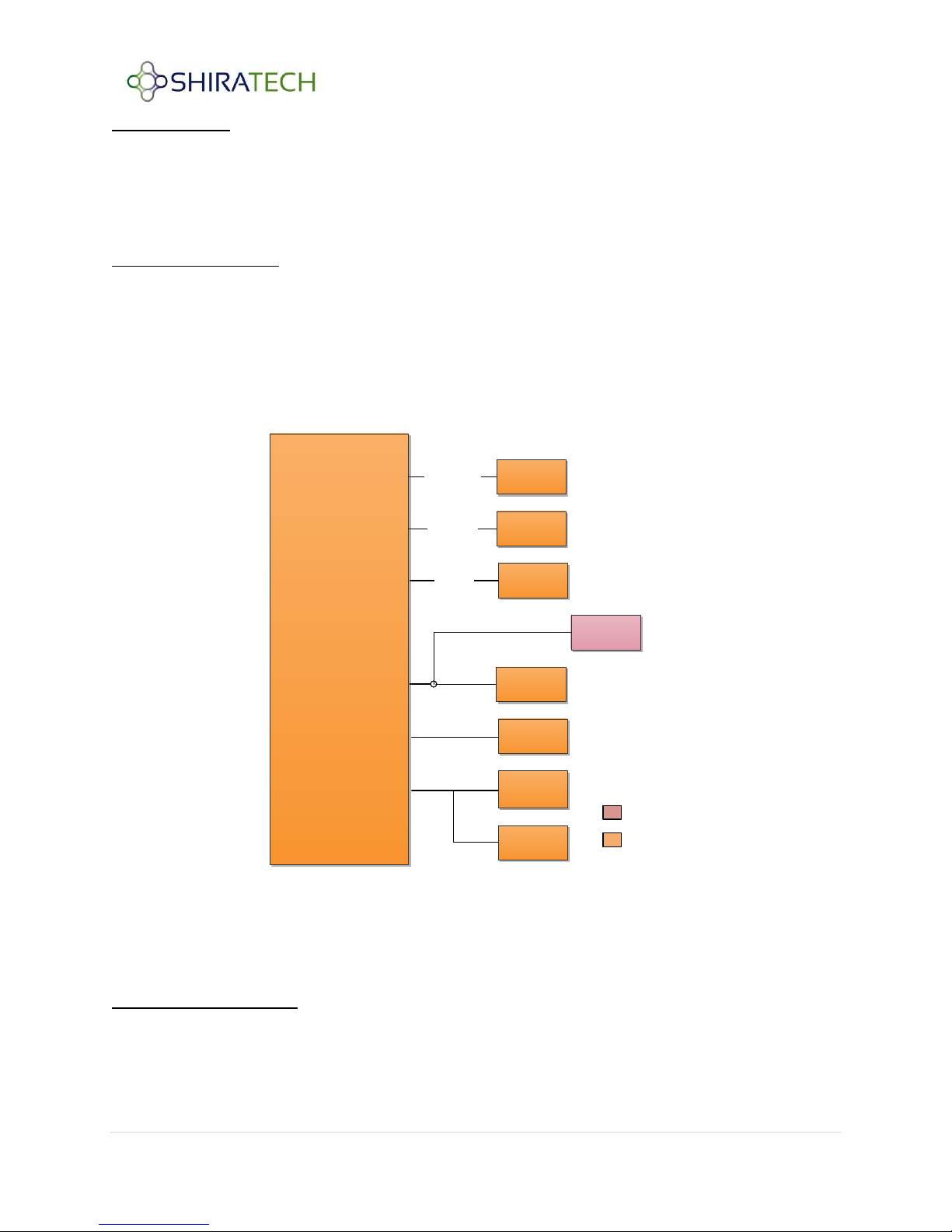
2.1 Power connectivity
The AT-501 uses a single power input of 3.3V from which all the other required voltages are taken. The
3.3V input is only directly used for power the processor I/Os. The Inlet power should be
Rise time: <= 3ms
Input voltage range: 3.3V +/- 5%
Typical power consumption: 0.5W
The AT-501 support low power modes, it can enter sleep mode by shutting down the main power source
leaving only a very small part active for possible wake up interrupt either internal or external.
For supporting these modes several additional lines are available:
VBAT – battery input for maintaining the RTC unit and Shutdown Controller within the processor. If not
used should be connected to 3.3V.
6 | AT-501 HW user manual 1.4
Figure 2 – AT-501 internal power scheme

Important:
VBAT must be high during power up for the processor to start working, so in case VBAT is connected to a
dedicated rechargeable battery or super cap, there must be a mechanism to provide the required
voltage during power up otherwise the processor will not start.
The AT-501 has an optional backup power source for the Real-Time-Clock. It can support an
approximately 1 hour of the RTC operation when the main power fails. The following figure describes
the AT-501 backup power. The backup power device, CBC3105, monitors the main power level and
when it drops below a configurable threshold it switch to its internal power source. During normal
operation the backup chip is recharge to its nominal power. In the basic ordering option the backup chip
is bypassed by a 0 ohm resistor. In this way an external power source can be connected to VBAT e.g.
high energy battery, to support longer backup time. For more details on that option contact
sales@shiratech.com .
WKUP (Input – pin 10 in the SO-DIMM connector) – The Wake Up line is used to wake up the system
using an external trigger, if unused should be left open. An internal pull up is assembled on the SOM.
Level 0 on the WKUP pin triggers the processor to wake up.
SHDN (Output - pin 12 in the SO-DIMM connector) – This pin enable the SW to shut down the power
after entering the SW and processor to sleep mode. A typical application connects the pin SHDN to the
shutdown input of the DC/DC Converter providing the main power supplies of the system.
Level 1 (3.3V) = Enable, Level 0 (0V) = Shutdown.
Note: If this pin is used along with a battery connected to the VBAT signal then the signal should be
pulled up to VBAT and not to regular 3.3V. In that way the signal remain valid even when the main
power is down.
PWR_ENB (Input – pin 30 in the SO-DIMM connector) this pin can be used to shut down the DC2DC chip
on the SOM. Asserting this line during shut down will reduce the system power dissipation
Level 1 (3.3V)= Enable, Level 0 (0V) = disable)
ADVREF - this pin is used for the reference voltage of the A/D pins if not used should be connected to
3.3V.
7 | AT-501 HW user manual 1.4

Atmel
SAMA5D
3.3 -> 1.8
3.3 -> 1.2
I/O
DDR
Core
CBC
3105
VBAT
SO-DIMM 200
3.3V
Shutdown
WakeUp
VBAT
Inlet
PLLFilter
SAMA5D
S
O
-
D
I
M
M
NRESET
3.3 V
Push-Button
NRESET
Figure 3 – AT-501 Backup Power scheme
2.2 Reset
The NRESET signal is an open-drain interface. It generates a reset on POR or on a reset event generated
by the SW. It also can be used as an input to an external reset source like a push-button.
The generated reset signal can be used to reset the system chips. The following figure describes the AT501 Reset signal.
Figure 4 - Reset Generation
8 | AT-501 HW user manual 1.4

SAM-A5
Micrel
ksz9031
Ethernet 0
RGMII
4 x TX
4 x RX
Controls
125 Mhz
25M
Int.
SO-DIMM 200
NReset
LEDS
RJ45
MAG
LEDS
GE Analog
FE
PHY
RMII
2 x TX
2 x RX
50 MHz
25M
MODULE A
RMII Analog
Control
Ethernet 1
2.3 Interfaces
The AT-501 offers a large variety of interfaces over the 200 pins SO-DIMM connector. The following
paragraphs describe the available interfaces along with guidance on how to connect and to use them.
For more information, review the SAMA5D3 data sheet.
2.3.1 Ethernet ports
The AT-501 support 1 Giga Ethernet port and one fast Ethernet port depending on the type of processor
assembled.
Figure 5 - Giga Ethernet & Fast Ethernet Interfaces
2.3.1.1 Giga Ethernet port
The AT-501 includes a build in 1GE interface (including physical layer chip) in all it models except the one
which includes the SAMA5D31 which does not support GE.
The Physical layer chip is connected via MDC/MDIO interface using the default PHY address is 0001 for
both interfaces.
The Giga Ethernet uses an RGMII interface to interconnect to the processor. The figure 5 describes the
Giga Ethernet interface. On the carrier board only the magnetics and connector should be placed. The
Giga Ethernet signals pairs should be routed from the PHY to the magnetic as differential pairs using 100
ohm impedance.
For the GE port the following signals are used as well:
Interrupt - PB-25 of the SAMA5 uses as an interrupt input for the Giga Ethernet PHY.
LEDs - Two led signals from the GE PHY are also connected to the SOM edge connector.
LED1 – Blinking Activity.
LED2- Link, on when there is link.
9 | AT-501 HW user manual 1.4

The led are connected to the GE PHY through a 470 ohm serial resistor.
Note: In case of the SAMA5D31, the pins used for GE should be left unconnected.
Figure 6 - Giga Ethernet schematics
2.3.1.2 Ethernet port
The Fast Ethernet interface is available for the D36, D35 and SAMA5D31 only. For the fast Ethernet port
there is no internal physical layer chip so it should be placed on the carrier board. The processor can be
connected to the physical layer using the RMII interface of the processor. The RMII runs on 50 MHz clock
that need to be provided to the processor by an external source.
The RMII signals should be connected directly to the CPU i.e. no serial resistors. Routing these signals to
the FE PHY should be done according to the RMII standard for proper operation.
2.3.1.3 MDC/MDIO
The Giga Ethernet MDC/MDIO signals are NOT available on the edge connector since the physical layer
chip is built in. The Fast Ethernet MDC/MDIO signals are available, MDIO (PC9) on pin 174, MDC (PC8) on
pin 175.
The MDC frequency is derived from the system clock and should not exceed 2.5MHz.
2.3.2 UART and USART
There are up to four USART and two UART interfaces dependent on PIO utilization and processor type.
The following paragraph describes the various options.
10 | AT-501 HW user manual 1.4

USART
Problem
Possible solution
USART 0
SD0 card detect is on
the same pin as TXD,
SD1 CD is on the RXD
This signals can be connected to other
GPIO and require a SW change,
alternatively, the SD can work without
that signal, can be detected via SDIO
bus
Multiplexed with CAN 0, SPI0 CS 1-3
USART 1
SCK uses the same pin
as the 1G interrupt pin
If GE is not assembled (D31), then all
pins are available otherwise require a
HW change on the SOM
USART 2
1 wire devices uses the
same pin as RXD
Can be ordered without the 1 wire –
special ordering item
USART 3
SCK not available
If required – connect Shiratech for
possible solutions
2.3.2.1 USARTs
The USART interface includes 5 signals RxD, TxD, CTS, RTS and SCK if synchronous operation is required.
Since the USART are multiplexed with other functions there are some limitations on the use of USART:
The USART main features are:
Programmable Baud Rate Generator
5-bit to 9-bit Full-duplex Synchronous or Asynchronous Serial Communications
o 1, 1.5 or 2 Stop Bits in Asynchronous Mode or 1 or 2 Stop Bits in Synchronous Mode
o Parity Generation and Error Detection
o By-8 or by-16 Over-sampling Receiver Frequency
o Optional Hardware Handshaking RTS-CTS
RS485 with Driver Control Signal
IrDA Modulation and Demodulation
Note: the USART can be used as SPI interface if required.
11 | AT-501 HW user manual 1.4

Figure 7 – UART – RS232 interface schematics
2.3.2.2 UART
The UART are available only on the D31, D35 and D36 only. If one of these chips is used then the UART
can be used under the following constrains:
UART 0 - Available only if the ISI interface is not used.
UART 1 – Available only if I2C0 is not used and if the ISI interface is not used.
The UART main features are:
Two-pin UART
Independent Receiver and Transmitter with a Common Programmable Baud Rate Generator
Even, Odd, Mark or Space Parity Generation
Parity, Framing and Overrun Error Detection
Automatic Echo, Local Loopback and Remote Loopback Channel Modes
Interrupt Generation
2.3.2.3 Debug Interface
The processor has an additional dedicated UART port for debug and control connected to the internal
debug controller (PB 30 and 31, Pins 117 and 118 in the SO-DIMM connector).
2.3.3 USB
The SAMA5D3 support 3 USB ports:
Port-A support USB 2.0 Host/Device OTG interface.
o This port can be programmed as Host or Device.
o It can also be programmed as an OTG interface.
o By monitoring the VUSB signal it can determine if it is connected to a Host or a device.
Note: For automatic detecting of the external device connected it is recommended to use the ID pin of
the USB interface and to connect it to a GPIO of the processor.
o This port should be used for connecting by the Atmel SAM-BA tool.
12 | AT-501 HW user manual 1.4

Type
A/B
Type
A
Current
Limiter
0.5A
SO-DIMM 200
USB A
USB B
5V USB
5V/0.5A
5V/0.5A
EN_A
EN_B
Over Current
VUSB Sense
USB
HUB
MODULE A MODULE B
Type
A
Current
Limiter
0.5A
EN
USB C
5V USB
5V/0.5A
Port-B supports USB 2.0 Host interface.
Port-C supports USB 2.0 Host interface.
The SAMA5D3 integrates the USB PHY so there is no need for external devices. To be compatible with
the AT-501 SW the following I/O need to be connected when using the USB interfaces:
• PD25 enable power for port A (pin 83).
• PD26 enable power for port B (pin 84)
• PD27 enable power for port C (pin 85).
• PD28 over current sense from all ports (pin 187).
• PD29 VUSB sense - power sense for port A (pin 186).
The USB ports can be extended to support additional USB ports, using an external USB hub. See figure
for an example of the USB connectivity used in the CB-20
Figure 8 – USB implantation example from the CB-20
13 | AT-501 HW user manual 1.4

2.3.4 High Speed Multi-Card Interface
The SAMA5D supports up to 3 HSMCI interfaces. All three interfaces are available on the edge
connector. The availability of the interfaces is dependent on the I/O configuration.
The HSMCI main features are:
MCI0 support up to 8 data bits (Only 4 bits are available on the edge connector).
MCI1 and MCI2 support up to 4 data bits.
Supports MMC, eMMC and SD cards.
Up to 50 MHZ clock.
Note – The Micro-SD card can be used as a booting memory. It has the highest priority on all other
nonvolatile memories.
The MCI interfaces can be used under the following constrains:
MCI 0 – Available, used for a bootable SD card.
o When used PD17(pin 80 on the connector) is used as card detect
MCI 1 - Available, cannot be used as a bootable SD source.
o When used PD18(pin 79 on the connector) is used as card detect
MCI 2 – Available if the RGB interface (24 bits mode) is not used.
Note: These pins are the ones currently supported by the CB-20 software, but they are not hardcoded
and any other GPIO can be used for these functions.
The following schematics show an implementation of a 4-bits Micro SD card. It is connected to the
SAMA5D3 MCI0 through the edge connector. The Micro-SD powered by a 3.3V power supply.
Figure 1 – Micro SD card implementation on the CB-20
2.3.5 LCD and touch screen support
The SAMA5D3 support an internal LCD controller with build in support for resistive touch screen.
14 | AT-501 HW user manual 1.4

2.3.5.1 LCD support
The SAMA5D3 has a build in LCD controller which can be connected directly to an external LCD using
RGB. The LCD has one display input buffer per overlay that fetches pixels through the dual AHB master
interface and a lookup table to allow palletized display configurations. The LCD controller is
programmable on a per overlay basis, and supports different LCD resolutions, window sizes, image
formats and pixel depths.
The LCD can be connected using either 16 bits RGB interface or 24 bits RGB interface.
In case 16 bits RGB
o LCD data (15:0) is available on PA(15-0)
o LCD control on PA(29-24).
For 24 bits RGB
o Use PC(15-10) and PE (28-27) for SW computability
In the CB-20 the LCD in connected via LVDS interface using an RGB to LVDS converter. Schematics are
available via support@shiratech.com
2.3.5.2 Resistive Touch screen
The SAMA5D3 has an ADC controller, which includes a Resistive Touchscreen Controller. It supports 4wire and 5-wire technologies with the following support:
Position and Pressure Measurement for 4-wire screens
Position Measurement for 5-wire screens
Average of up to 8 measures for noise filtering
The touch interface is using AD(0-4) which are available over pins 181-185 in the SO-DIMM connector.
See below touch screen connectivity sample for the CB-20
Figure 10 – Touch screen connectivity example
Note: if these pins are not used, they are set to inputs with internal pull up.
15 | AT-501 HW user manual 1.4

2.3.6 CAN
The AT-501 supports up to two CAN interfaces depending on the processor type (available only on the
D34 and D35). The CAN interfaces are available under the following constrains:
CAN 0 - If USART 0 CTS, SCK are used or if SPI0-CS(1-2) then CAN 0 cannot be used.
CAN 1 - no limitations.
2.3.7 I2C
There are up to three I2C interfaces available on the SAMA5D3. All three interfaces are available on the
edge connector. The availability of the I2C interfaces is dependent on the I/O configuration. The I2C
interface requires pull ups on both lines, the pull ups should be placed on the carrier board.
The I2C main features are:
One, Two or Three Bytes for Slave Address
Sequential Read-write Operations
Master, Multi-master and Slave Mode Operation
Bit Rate: Up to 400 Kbits
General Call Supported in Slave mode
MBUS Quick Command Supported in Master Mode
Connection to DMA Controller (DMA) Channel Capabilities Optimizes Data Transfers
The I2C ports are available under the following conditions:
I2C 0 – Available only when UART 1 is not used and the ISI interface is not used.
I2C 1 - Available only if SPI 1 CS 1 and 2 are not used.
I2C 2 – Available only if the ISI interface is not used.
2.3.8 SPI
There are up to two SPI interfaces dependent on PIO utilization. Both interfaces are available on the SODIMM 200 connector.
The SPI main features are:
Programmable as Master or Slave.
Up to 25 MHz clock.
Up to 4 chips select signal that can be configure as discreet or as a 4 bits logical combination.
It is recommended to put a serial resistor on the clock signal close the SO-DIMM connector. No need to
put pull-up resistors on the data signals.
2.3.9 A to D Convertor
The ADC is based on a 12-bit Analog-to-Digital Converter (ADC) managed by an ADC Controller. It also
integrates a 12-to-1 analog multiplexer, making possible the analog-to-digital conversions of 12 analog
lines. The conversions extend from 0V to the voltage carried on pin ADVREF (up to 3.3V).
The ADC converter supports the following features:
o 12-bit Resolution
16 | AT-501 HW user manual 1.4

o 1 MHz Conversion Rate
o Wide Range Power Supply Operation
o Selectable Single Ended or Differential Input Voltage
o Programmable Gain For Maximum Full Scale Input Range 0 – VDD
o Integrated Multiplexer Offering Up to 12 Independent Analog Inputs
o Individual Enable and Disable of Each Channel
o Hardware or Software Trigger
o External Trigger Pin
ADVREF (Pin 190) is the Reference voltage input for the ADC function
2.3.10 JTAG
The AT-501 has a JTAG interface that can be used either for JTAG testing or for connecting an ICE. The
selection between the two modes is done using setting JTAGSEL pin 8 in the SO-DIMM connector to the
right mode.
The JTAG connector is a 20 pins connector enables JTAG card testing or ICE emulation(you should use
the same pin-out for supporting J-link emulator).
JTAGSEL is used for selecting the right mode, for normal mode or ICE – open, ‘1’ for JTAG test
2.4 Mechanical considerations
The AT-501 SoM is 47.5x67.6mm module. It is connected to the carrier board using a SO-DIMM
connector and it has two holes for additional mechanical support (see dimensions below).
17 | AT-501 HW user manual 1.4
Figure 11 – JTAG emulator interface

U22
Figure 12 – AT-501 CS view
- The height of devices in the PS is up to 1mm with the exception of U22 which is 1.4mm.
- The supporting holes diameter is 3mm.
18 | AT-501 HW user manual 1.4
Figure 13 – AT-501 PS view

Pin
Card
pinout
Dedicated
Functionality
Type
Description
1
3.3V
Power
2
3.3V
Power
3
3.3V
Power
4
3.3V
Power
5
GND
Ground
6
VBAT
Power
Should be connected to external
battery or to 3.3 power source if
battery is not used
7
USB-C DP
USB-C
8
JTAGSEL
JTAG
input
JTAG Selection, select between
JTAG and ICE. When open normal
mode or J-link emulator. '0' for JTAG
2.4.1 SO-DIMM connector
The AT-501 uses an SO-DIMM interface for connecting the SOM. The carrier board should use a 1.8V
DDR2 SO-DIMM connector. The connector comes in different heights according the need.
In the CB-20 the SO-DIMM connector is 1473005-4 from TE connectivity. Any other compatible
connector can be used.
2.5 Pin assignment
The SO-DIMM connector offers 200 pins which are used for:
Power
GPIOs which can be used either as GPIOs or as various interfaces
Fixed interfaces like GE and USB
RFU - un used pins reserved for future use.
The following table shows the pin assignment of the connector. The following tables will show the
options for each GPIO. The SAMA5D3 processor offers 5 banks of GPIOs each contain 32 bits, PA, PB,
PC, PD and PE. The following tables will show the options for each bank. Note that not all options are
possible.
Note: Shiratech offers a pin configuration tool (available at Shiratech web site) which offers an easy
way to configure the pin assignment of the module according to the functions need. The tool also
provide additional information on the pin out and multiplexing options.
2.5.1 SO-DIMM 200 Pins assignment
- Gray power and ground lines.
- Red dedicated I/Os
- Green un used pins should be left open
- Blue GPIOs
19 | AT-501 HW user manual 1.4

test
9
USB-C DN
USB-C
10
WKUP
power control
Input
The wake-up input (WKUP0)
connect to any push-buttons or
signal that wake up the processor.(if
using VBAT then is should be
connected to VBAT and not to
regular VCC)
11
GND
Ground
12
SHDN
power control
Output
Used for shut down the system
external peripherals , internal pull up
on the SOM(This signal use VBAT,
do not connect to regular VCC)
13
USB-B DP
USB-B
14
RFU
Not used
15
USB-B DN
USB-B
16
NRST
Reset
Reset pin, can be used for reset the
processor or as a reset signal to the
carrier board
17
GND
Ground
18
NTRST
JTAG
Input
JTAG Test Reset Signal
19
DIBP
Soft modem
Soft Modem Signal
20
TDI
JTAG
JTAG - Test Data In
21
DIBN
Soft modem
Soft Modem Signal
22
TCK
JTAG
Input
JTAG Test clock Signal
23
GND
Ground
24
TMS
JTAG
Input
JTAG test mode select
25
USB-A DP
USB-A
26
TDO
JTAG
Output
JTAG Test Data Out
27
USB-A DN
USB-A
28
RTCK
JTAG
Output
JTAG Returned Test Clock
29
GND
Ground
30
PWR_EN
power control
input
Enable the DC2DC on the SOM
card, Integrated pull up on the SoM if
not required leave open
31
RFU
Not used
32
RFU
Not used
33
RFU
Not used
34
RFU
Not used
35
PE16
GPIO 36
PE17
GPIO
37
PE18
GPIO
38
PE19
GPIO
39
PE20
GPIO
20 | AT-501 HW user manual 1.4

40
PE21
GPIO
Does not use when the SOM
includes a NAND flash!!
41
GND
Ground
42
GND
Ground
43
PE22
GPIO
Does not use when the SOM
includes a NAND flash!!
44
PE23
GPIO 45
PE24
GPIO 46
PE26
GPIO 47
RFU
Not used
48
PE31
GPIO
49
PD30
GPIO
50
PD31
GPIO
51
GND
Ground
52
GND
Ground
53
PC30
GPIO 54
PC31
GPIO
Fast interrupt
55
PC28
GPIO 56
PC29
GPIO 57
PC26
GPIO 58
PC27
GPIO 59
PA22
GPIO 60
PA23
GPIO
61
3.3V
Power
62
3.3V
power 63
PA20
GPIO 64
PA21
GPIO 65
PA18
GPIO 66
PA19
GPIO 67
PA16
GPIO 68
PA17
GPIO 69
PD14
GPIO 70
PD15
GPIO 71
PD16
GPIO 72
PB12
GPIO
73
PB23
GPIO
74
GND
Ground
75
PB21
GPIO 76
PB24
GPIO 77
PB19
GPIO 78
PB22
GPIO
21 | AT-501 HW user manual 1.4

79
PD18
MCI1
GPIO
When using MCI1 for SD this pin is
used for SD card detect (MCI1),note
this pin location can be modified by
SW if the pin is requirted for another
use
80
PD17
MCI0
GPIO
When using MCI0 for SD this pin is
used for uSD card detect (MCI0),
note this pin location can be
modified by SW if the pin is requirted
for another use
81
PE29
GPIO 82
PB20
GPIO
83
PD25
USB-A
O
When using USB port A, this pin is
used for USB port A power drive
enable
84
PD26
USB-B
O
When using USB port B, this pin is
used for USB port B power drive
enable
85
PD27
USB-C
O
When using USB port C, this pin is
used for USB port C power drive
enable
86
PB25
GMAC
GPIO
When using the GE port this pin is
used for Giga Ethernet interrupt
87
3.3V
Power
88
3.3V
Power 89
PB29
GPIO
90
PB28
GPIO
91
PB27
GPIO 92
PB26
GPIO 93
PB10
GPIO
94
GND
Ground
95
PD10
GPIO 96
PD11
GPIO 97
PD12
GPIO 98
PD13
GPIO
99
GND
Ground
100
RFU
Not used
101
PC22
GPIO
102
PC25
GPIO 103
PC23
GPIO 104
PC24
GPIO 105
PA31
GPIO 106
PA30
GPIO
107
GND
Ground
108
PD1
GPIO 109
PD0
GPIO
22 | AT-501 HW user manual 1.4

110
PD9
GPIO
111
PD2
GPIO 112
PD3
GPIO
113
PD4
GPIO
114
GND
Ground
115
PB15
GPIO 116
PB14
GPIO 117
PB31
Debug port
GPIO
Debug port - DGB TX
118
PB30
Debug port
GPIO
Debug port - DBG RX
119
GND
Ground
120
PC16
GPIO 121
PC17
GPIO 122
PC18
GPIO 123
PC21
GPIO 124
PC19
GPIO
125
PC20
GPIO
126
GND
Ground
127
3.3V
Power
128
3.3V
Power
129
PA0
GPIO 130
PA1
GPIO 131
PA2
GPIO 132
PA3
GPIO 133
PA4
GPIO 134
PA5
GPIO
135
GND
Ground
136
PA6
GPIO
137
PA7
GPIO
138
PA8
GPIO 139
PA9
GPIO 140
PA10
GPIO 141
PA11
GPIO
142
GND
Ground
143
PA12
GPIO 144
PA13
GPIO 145
PA14
GPIO
146
PA15
GPIO
147
GND
Ground
148
PC14
GPIO
149
PC13
GPIO
150
PC12
GPIO 151
PC11
GPIO
152
PC10
GPIO
23 | AT-501 HW user manual 1.4

153
PC15
GPIO
154
GND
Ground
155
PE27
GPIO
156
PE28
GPIO
157
PA25
GPIO 158
PD19
GPIO 159
PA24
GPIO 160
PA26
GPIO
161
GND
Ground
162
PA27
GPIO 163
PA29
GPIO 164
PA28
GPIO 165
LED1
GMAC
166
LED2
GMAC
167
RFU
Not used
168
RFU
Not used
169
PC2
GPIO 170
PC3
GPIO 171
PC6
GPIO 172
PC5
GPIO 173
PC7
GPIO
174
PC9
GPIO
MDIO - When using Ethernet, Can
be used to configure external
phy/switch
175
PC8
GPIO
MDC - When using Ethernet, Can be
used to configure external
phy/switch
176
PC4
GPIO
177
PE30
EMAC
GPIO
When using the Ethernet port this
pin is Fast Ethernet interrupt
178
GND
Ground
179
PC0
GPIO 180
PC1
GPIO 181
PD20
GPIO 182
PD21
GPIO 183
PD22
GPIO
184
PD23
GPIO
185
PD24
GPIO
186
PD29
USB-A
GPIO
When using USB port A, this pin is
used for power sense
187
PD28
USB
GPIO
over current sense from all USB
ports
188
GND
Ground
24 | AT-501 HW user manual 1.4

189
PE25
1 wire
The 1 wire bus used also by the 1
wire chip located on the SoM, if the
other USARTs are not enough, the
SOM can be ordered with out the 1
wire device
190
ADVREF
Power
reference voltage for A/D, if not used
connect to 3.3V
191
GND
Ground
192
ET0-Tx2+
GMAC
GE
193
ET0-Tx1+
GMAC
GE 194
ET0-Tx2-
GMAC
GE 195
ET0TX1-
GMAC
GE 196
ET0RX2+
GMAC
GE 197
ET0RX1+
GMAC
GE 198
ET0RX2-
GMAC
GE 199
ET0RX1-
GMAC
GE 200
GND ETH
Ground
25 | AT-501 HW user manual 1.4

Signal
Configuration
Option 1
Option 2
Option 3
PA0
PA0
LCD-DA0
PA1
PA1
LCD-DA1
PA2
PA2
LCD-DA2
PA3
PA3
LCD-DA3
PA4
PA4
LCD-DA4
PA5
PA5
LCD-DA5
PA6
PA6
LCD-DA6
PA7
PA7
LCD-DA7
PA8
PA8
LCD-DA8
PA9
PA9
LCD-DA9
PA10
PA10
LCD-DA10
PA11
PA11
LCD-DA11
PA12
PA12
LCD-DA12
PA13
PA13
LCD-DA13
PA14
PA14
LCD-DA14
PA15
PA15
LCD-DA15
PA16
PA16
LCD-DA16- Not
used
ISI_D0
PA17
PA17
LCD-DA17 - Not
used
ISI_D1
PA18
PA18
LCD-DA18 - Not
used
I2C2 - TWD
ISI_D2
PA19
PA19
LCD-DA19 - Not
used
I2C2 - TWCK
ISI_D3
PA20
PA20
LCD-DA20 - Not
used
PWMH0
ISI_D4
PA21
PA21
LCD-DA21 - Not
used
PWML0
ISI_D5
PA22
PA22
LCD-DA22 - Not
used
PWMH1
ISI_D6
PA23
PA23
LCD-DA23 - Not
used
PWML1
ISI_D7
PA24
PA24
LCD-PWM
PA25
PA25
LCD-DISP
PA26
PA26
LCD-VSYNC
2.5.2 Port A options
Configuration options for port A (for more details see the SAMA5D3 user manual).
Not available pins – pins which are not connected to the 200 pin connector and so cannot be
used.
26 | AT-501 HW user manual 1.4

PA27
PA27
LCD-HSYNC
PA28
PA28
LCD-PCK
PA29
PA29
LCD-DEN
PA30
PA30
I2C0 – TWD
UART1 - RXD
ISI_VSYNC
PA31
PA31
I2C0 - TWCK
UART1 - TXD
ISI_HSYNC
Signal
Configuration
Option 1
Option 2
Option 3
PB0
Not available
GTX0
PWMH0 PB1
Not available
GTX1
PWML0 PB2
Not available
GTX2
TK1
PB3
Not available
GTX3
TF1
PB4
Not available
GRX0
PWMH1 PB5
Not available
GRX1
PWML1 PB6
Not available
GRX2
TD1 PB7
Not available
GRX3
RK1 PB8
Not available
GTXCK
PWMH2
PB9
Not available
GTXEN
PWML2
PB10
PB10
GTXER
RF1 PB11
Not available
GRXCK
RD1 PB12
PB12
GRXDV
PWMH3
PB13
Not available
GRXER
PWML3
PB14
PB14
GCRS
CAN1 - RX
PB15
PB15
GCOL
CAN1 - TX
PB16
Not available
GMDC
PB17
Not available
GMDIO
PB18
Not available
G125CK
PB19
PB19
MCI1_CDA
GTX4 PB20
PB20
MCI1_DA0
GTX5
PB21
PB21
MCI1_DA1
GTX6
PB22
PB22
MCI1_DA2
GTX7 PB23
PB23
MCI1_DA3
GRX4 PB24
PB24
MCI1_CK
GRX5
PB25
PB25
USART1 - SCK1
GRX6
2.5.3 Port B options
Configuration options for port B (for more details see the SAMA5D3 user manual).
Note available pins – pins which are not connected to the 200 pin connector and so cannot be
used.
27 | AT-501 HW user manual 1.4

PB26
PB26
USART1 - CTS1
GRX7
PB27
PB27
USART1 - RTS1
G125CKO
PB28
PB28
USART1 - RXD1
PB29
PB29
USART1 - TXD1
PB30
Debug- RXD
Debug- RXD
PB31
Debug- TXD
Debug- TXD
Signal
Configuration
Option 1
Option 2
Option 3
PC0
PC0
E-TX0
TIOA3 PC1
PC1
E-TX1
TIOB3
PC2
PC2
E-RX0
TCLK3
PC3
PC3
E-RX1
TIOA4 PC4
PC4
E-TXEN
TIOB4 PC5
PC5
E-CRSDV
TCLK4 PC6
PC6
E-RXER
TIOA5 PC7
PC7
E-REFCK
TIOB5
PC8
PC8
E-MDC
TCLK5
PC9
PC9
E-MDIO
PC10
MCI2_CDA
MCI2_CDA
LCD-DAT20
PC11
MCI2_DA0
MCI2_DA0
LCD-DAT19
PC12
MCI2_DA1
MCI2_DA1
TIOA1
LCD-DAT18
PC13
MCI2_DA2
MCI2_DA2
TIOB1
LCD-DAT17
PC14
MCI2_DA3
MCI2_DA3
TCLK1
LCD-DAT16
PC15
MCI2_CK
MCI2_CK
PCK2
LCD-DAT21
PC16
PC16
SSC0-TK
PC17
PC17
SSC0-TF
PC18
PC18
SSC0-TD
PC19
PC19
SSC0-RK
PC20
PC20
SSC0-RF
PC21
PC21
SSC0-RD
PC22
PC22
SPI1_MISO
PC23
PC23
SPI1_MOSI
PC24
PC24
SPI1_SPCK
PC25
PC25
SPI1_NPCS0
PC26
PC26
SPI1_NPCS1
I2C1 - TWD
ISI_D11
2.5.4 Port C options
Configuration options for port C (for more details see the SAMA5D3 user manual).
Not available pins – pins which are not connected to the 200 pin connector and so cannot be
used.
28 | AT-501 HW user manual 1.4

PC27
PC27
SPI1_NPCS2
I2C1 - TWCK
ISI_D10
PC28
PC28
SPI1_NPCS3
PWMFI0
ISI_D9
PC29
PC29
UART0 - RXD
PWMFI2
ISI_D8
PC30
PC30
UART0 - TXD
ISI_DPCK
PC31
FIQ
FIQ
PMWFI1
Signal
Configuration
Option 1
Option 2
Option 3
PD2
MCI0_DA1
MCI0_DA1
PD3
MCI0_DA2
MCI0_DA2
PD4
MCI0_DA3
MCI0_DA3
PD5
Not available
MCI0_DA4
TIOA0
PMWH2
PD6
Not available
MCI0_DA5
TIOB0
PMWL2
PD7
Not available
MCI0_DA6
TCLK0
PMWH3
PD8
Not available
MCI0_DA7
PMWL3
PD9
MCI0_CK
MCI0_CK
PD10
PD10
SPI0_MISO
PD11
PD11
SPI0_MOSI
PD12
PD12
SPI0_SPCK
PD13
PD13
SPI0_NPCS0
PD14
PD14
USART0 - SCK
SPI0_NPCS1
CAN0 - RX
PD15
PD15
USART0 - CTS
SPI0_NPCS2
CAN0 - TX
PD16
PD16
USART0 - RTS
SPI0_NPCS3
PWMFI3
PD17
PD17
USART0 - RXD
PD18
PD18
USART0 - TXD
PD19
PD19
ADTRG
PD20
PD20
AD0 - touch screen
PD21
PD21
AD1 - touch screen
PD22
PD22
AD2 - touch screen
PD23
PD23
AD3 - touch screen
PD24
PD24
AD4 - touch screen
PD25
PD25
AD5
PD26
PD26
AD6
PD27
PD27
AD7
PD28
PD28
AD8
PD29
PD29
AD9
2.5.5 Port D options
Configuration options for port D (for more details see the SAMA5D3 user manual).
Not available pins – pins which are not connected to the 200 pin connector and so cannot be
used.
29 | AT-501 HW user manual 1.4

PD30
PD30
AD10
PCK0
PD31
PD31
AD11
PCK1
Signal
Configuration
Option 1
Option 2
Option 3
PE2
Not available
A2
PE3
Not available
A3
PE4
Not available
A4
PE5
Not available
A5
PE6
Not available
A6
PE7
Not available
A7
PE8
Not available
A8
PE9
Not available
A9
PE10
Not available
A10
PE11
Not available
A11
PE12
Not available
A12
PE13
Not available
A13
PE14
Not available
A14
PE15
Not available
A15
SCK3 PE16
PE16
A16
USART3 - CTS
PE17
PE17
A17
USART3 -RTS
PE18
PE18
A18
USART3 -RXD
PE19
PE19
A19
USART3 -TXD
PE20
PE20
A20
USART2 - SCK
PE21
PE21
A21/NANDALE
PE22
PE22
A22/NANDCLE
PE23
PE23
A23
USART2 -CTS
PE24
PE24
A24
USART2 -RTS
PE25
1 wire
A25
USART2 -RXD
PE26
PE26
NCS0
USART2 -TXD
PE27
PE27
NCS1
TIOA2
LCD-DAT22
PE28
PE28
NCS2
TIOB2
LCD-DAT23
PE29
PE29
NWR1/NBS1
TCLK2 PE30
PE30
NWAIT
PE31
IRQ
IRQ
PWML1
2.5.6 Port E options
Configuration options for port E (for more details see the SAMA5D3 user manual).
Not available pins – pins which are not connected to the 200 pin connector and so cannot be
used.
30 | AT-501 HW user manual 1.4

3 AT-501 System overview
3.1 Cortex-A5 Processor
The AT-501 uses Atmel's SAMAD5 ARM Cortex-A5 based CPU as the modules controller. The SAMA53 is
a family of CPU which implement the ARMv7 architecture and run 32 bits instructions. It includes an FPU
(Not NEON) which is tightly integrated into the processor pipeline.
The SAMAD5 support different flavors e.g. Single/dual Ethernet, enhanced graphic accelerator, LCD and
more. All those flavors are footprint compatible and can be supported by the AT-501 module.
The SAMAD5 main features are:
536 MHZ core frequency
32 Kbytes data and instruction cache
Fully integrated MMU.
Fully integrated FPU (VFPv4)
System running at 166 MHz
Integrated RTC, POR and WDT
Low power mode
Multiplex peripherals bus
324 pins BGA package
3.2 Memories
The AT-501 includes varieties of memory options to support booting, program execution and ID. The
following figure describes the memories mapping of the AT-501.
DDR2
32 bits Data bus.
256Mbytes memory space (Can be upgraded up to 512 Mbytes).
166 MHz system clock.
Uses for SW execution.
NAND
8 bits data bus.
2Gbits (256Mbytes), a larger NAND memory 4, 8 and 16GBits are supported(ordering option).
Uses for boot and data storage.
NOR flash
Not available. For more information contact sales@shiratech.com
31 | AT-501 HW user manual 1.4
SAM-A5
NAND
MMC 0
SOM
Carrier
uSD
eMMC
D[0 -7]
NOR
Data Flash
SPI 0
One Wire
Secure
Boot
DDR 2
DDR 2
D[0 – 15]
D[16 – 31]
1-Wire EEPROM,
The AT-501 includes 128 bytes E2PROM memory (DS2431P – by Maxim), of which the first 64bytes
are reserved for card information, the additional 64 byes can be used by the end user for data
storage.
Micro-SD (Not on SOM)
Uses the SAMA53's MCI0 interface.
Implements 4 data bits.
Up to 25 MHz clock.
Can be used as Booting memory.
eMMC (iNAND) – optional
The AT-501 can be equipped with 4 or 8 GB eMMC device. The device can be used both for data and
software.
Uses the SAMAD5 MCI0 interface.
Implements 8 data bits.
32 | AT-501 HW user manual 1.4
Figure 13 – AT-501 Memory

Up to 25 MHz clock.
The software does not support two MMC devices on the same bus. In case two devices are available
only one of them will be detected by the processor and the other one will be unreachable.
One-Wire memory device
Maxim's DS2431P.
Uses for ID storage.
Note: The one-wire chip contains information about the board, this information should not be changed
by the end user. In case the information will be changed warranty will not be available for the module.
33 | AT-501 HW user manual 1.4
 Loading...