

Page 1
kangaroo
Det
、
Feeding
Service
Enteral
Pump
Manual
Page 2

woo
Page 3
table
of
contents
section
1.
general
—product
2.
maintenance
一
routine
ーcleanind
—housing
—drop
—rotorassembiy
—calibration
—additional
人
—recommended
—charger
—ambulatory
3.
circuit
—charger
—ambulatory
4.
printed
—charger
—ambulatory
detector
description
—AC
—Supply
—charge
一 quick
—Microprocessor
—power
—power-on
—reset
一
battery
一
touch
—LED
ーdrop
一
motor
—fail-safe
一
rotor
—frame
—pump
—audio
—
language
—schematic
—assembly
一
parts
—schematic
—assembly
information
description
maintenance
し に に ーー に ーー に トト
.............................,....,........2.
...........
tests . eernenennnes
base
pump
base
to
DC
voltage
current
charge
pump
supply
circuit
monitoring
panel
display
detector
detection
detection
set
alarm
circuit
base
list
pump
.....................................
:.................
ーー
トド に に
トト に トート
.......................,,........,........
...........................
1.1.1.
スト
トレ
トレ
2...
ーー トー
rea
performance
assembly
assembly
.
conversion
output
outpul
control . «νεο
test
......................,....
........................,.........
...............................
eee
................................
...............................
..................
εν
ενω
νεο
0...
νε ω νε
ων
..... ーー 10-13
....................................
........................
circuit
................................,..
1.10...
.
............................,....
. .
ντ
..
..
τν νε ω νε
ων
ενω
ενω
ων
νεο
ον
νοκ
εννοω
가
아게 기가 에 세세 우게
44.
eee,
εκ εκ ο νε
νεο ν ον
sneen
...............................,....
detection
.................................
......................,...............
selection
.................,..........,....
boards
..........................................
diagram
diagram
.
ee
diagram
Чадгат
.................................
...............,...........,.....
krrenkekre
.................................
........
еее
es
A
ニー
ューーー
0.1.1...
e
rr
ενω κ νεος
erekkee
eee
ων ον
마이
아아
enkes
νε κ νο ον
eee
page
1,2
3
3
3
3
3
4
4
4,5
6,7
8
8
9
9
9
9.
9
10
10
10,11
1
11
11
1
12
12
12
19
12
12
12
13
14,
15
14
15
15
16-18
16,
17
18
5.
final
assembly
—chargerbase
—parts
—partS
—
атьщаюгу
—parts
一
Parts
6.
specifications
7.
troubleshooting
8.
factory
service/ordering
......................
breakdown
HS...
ec
ритр
diagram
......... ο νεο
............................
ον
κενο
0...
εν
εννοω
cee
ων
εν ων
teens
χε
breakdowndiağram............................
SE
κ
........................................
guide
................................
information
..................
νο
ον ον
19,
20
19
20
21,
22
21
22
23,
24
25
26
Page 4
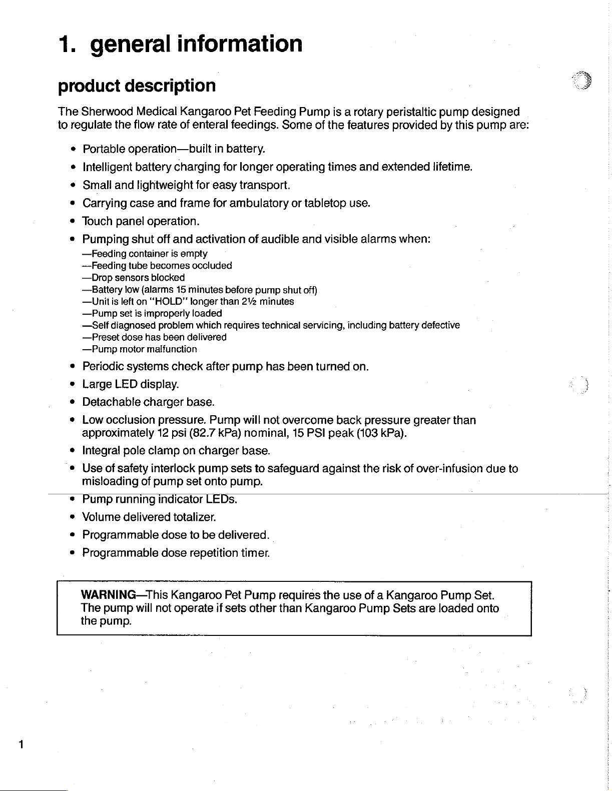
1.
general
information
product
The
Sherwood
to
regulate
Portable
Intelligent
Small and
Carrying
Touch
Pumping
—Feeding
—Feeding
—Drop
—
—
—Pump
—Self
—Preset
—Pump
Periodic
the
panel
sensors
Battery
Unit
is
diagnosed
description
Medical
flow
operation—built
battery
lightweight
case
operation.
shut
container
tube
low
(alarms
left
on
“HOLD”
set
is
improperly
dose
has
motor
malfunction
systems
Kangaroo
rate
of
charging
and
frame
off
and
is
empty
becomes
blocked
15
problem
been
check
enteral
for
activation
occluded
minutes
longer
loaded
which
delivered
after
Pet
Feeding
feedings.
in
battery.
for
longer
easy
transport.
for
ambulatory
of
before
than
2V2
requires
pump
Pump
Some
operating
or
tabletop
audible and
pump
shut
off)
minutes
technical
has
servicing,
been
is a rotary
of
the
features
times and
use.
visible
including
turned
alarms
on.
peristaltic
provided
extended
pump
by
lifetime.
when:
battery
defective
designed
this
pump
are:
Large
Detachable
Low
approximately
Integral
Use
misloading
Pump
Volume
Programmable
Programmable
WARNING—This
The
the
LED
display.
occlusion
pole
of
safety
running
delivered
pump
pump.
will
charger
pressure.
12
psi
clamp
on
interlock
of
pump
indicator
totalizer.
dose
dose
Kangaroo
not
operate
base.
Pump
(82.7
kPa)
charger
pump
set
to
repetition
sets
onto
pump.
LEDs.
be
delivered.
Pet
if
sets
timer.
will
not
overcome
nominal,
base.
to
safeguard
Pump
other
requires
than
15
PSI
against
the
Kangaroo
back
peak
use
pressure
(103
kPa).
the
risk
of
of a Kangaroo
Pump
Sets
greater
over-infusion
are
than
Pump
loaded
due
Set.
onto
to
Page 5
"
10
9
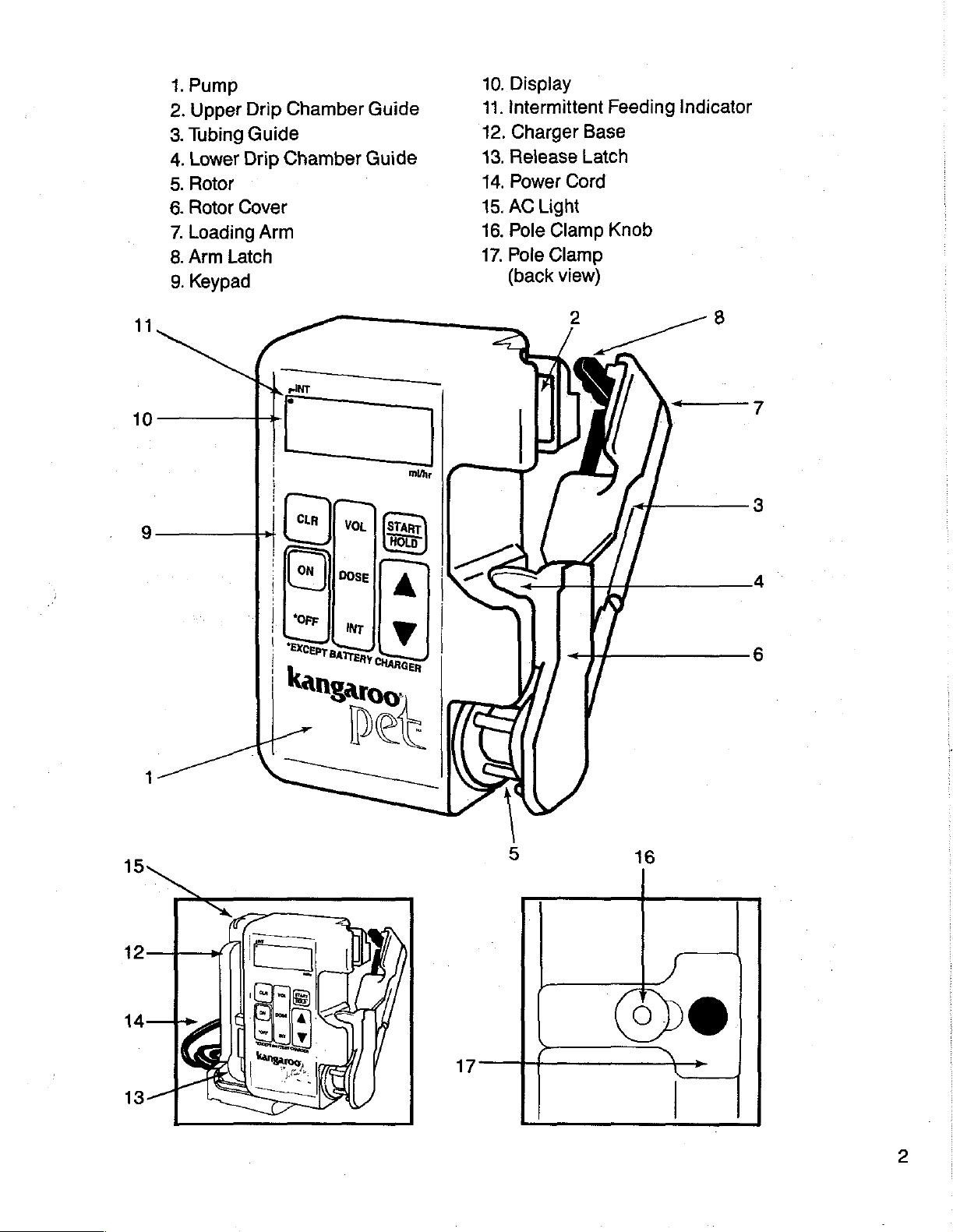
1.
2.
3.
4.
5.
6.
7.
8.
9.
tS
Pump
Upper
Tubing
Lower
Rotor
Rotor
Loading
Arm
Keypad
Drip
Guide
Drip
Cover
Latch
Chamber
Chamber
Arm
Guide
Guide
10.
Display
intermittent
11.
Charger
12.
Release
13,
Power
14.
Light
AC
15.
Clamp
Pole
16.
Clamp
Pole
17.
(back
view)
Base
Latch
Cord
Feeding
Knob
Indicator
15
12
14
13-7
Page 6
2.
maintenance
routine
Routine
rotor
and
CAUTION:
to
maintenance
maintenance
rollers.
Disconnect
prevent
electrical
consists
cleaning
—Disconnect
—Do
not
—A
mild
—lf
necessary, a hypochlorite
be
used
the
plastic
charger
immerse
pump
detergent
for
cleaning
and
tabelling
or
isopropyl
housing
—Clean
remove
—Avoid
base
—Keep
outside
excess
excess
surfaces
moisture
moisture
connectors
pump
and
charger
shock.
base
from
in
cleaning
the
pump;
of
the
with a damp
near
base
primarily
the
pump
AC
power
solution
alcohol
solution
however,
pump
drop
detector,
upright
of
preventing
from
the
source
may
be
(10
parts
repeated
and
charger
cloth
or
loading
as
much
AC
before
used
for
water
cleaning
base.
sponge;
arm
as
possible
and
cleaning
power
source
cleaning
general
to 1 part
with
wring
cloth
bearing,
spillage
before
cleaning.
household
this
solution
or
sponge
and
pump
on
the
cleaning
bleach)
can
thoroughly
and
charger
housing,
can
also
damage
to
drop
—Clean
alcohol
—Be
sure
rotor
—
Remove
from
the
-—Loosen
—Clean
—Be
sure
—To
replace
shaft
ーPush
—
Place
place
detector
the
drop
sensors
sensor
areas
assembly
two
rotor
shield
rotor
rotor
set
screw
rollers
rotor
the
(DO
thoroughly
all
parts
rotor,
into
rotor
NOT
of
align
. ]
place
shield
OVERTIGHTEN)
in
are
screws
with a 54”
with
rotor
are
set
and
into
the
upper
clear
with a Phillips
warm
completely
screw
tighten
its
proper
on
set
drip
chamber
allen
wrench
soapy
dry
hub
of
screw
position
screwdriver
and
water,
or
before
rotor
with
(DO
NOT
and
tighten
guide
with
cotton
and
gently
isopropyl
putting
the
pull
alcohol
it
back
flattened
OVERTIGHTEN)
the
two
swabs
lift
the
rotor
forward
if
onto
section
screws
and
isopropyl
rotor
shield
off
shaft
necessary
shaft
of
the
motor
that
hold
away
it
in
Page 7
2.
maintenance
(cont.)
CARE
TO
ALCOHOL
PUMP
SHOULD
ELECTRICAL
OR
HOUSING.
OTHER
calibration
There
is
no
calibration
additional
Motor
turning,
Motor
speed
stops,
cycle
can
and
time
RATE
300
400
BE
TAKEN
COMPONENTS
STRONG
required
tests
be
verified
then
starts
is
as
follows:
(ml/hr)
10
50
125
THAT
NO
COULD
CLEANSERS
for
the
by
measuring
turning
SOLUTION
RESULT.
Kangaroo
the
again.
in
backpack
41.040
8.208
9.850
4.104
3.078
COULD
Pet
time
Time
GETS
INSIDE
PROLONGED
RESULT
pump.
elapsed
(seconds)
from
NOT
THE
EXPOSURE
IN
DAMAGE
when
in
backpack
45.000
9.000
10.800
4.500
3.375
PUMP,
the
motor
AS
TO
TO
starts
DAMAGE
THE
The
tolerance
instruments.
accuracy
for
Manual
and
consistency. A tolerance
measurement.
Pressing
in
the
before
selection
the
pump’s
normal
portion
CLR
language
operation
alarms
Internal
The
The
microprocessor
cell
No
With
when
System
The
the
significantly
Circuit
pump
will
possible
in
the
battery
Set
Alarm
no
feeding
START/HOLD
Error
pump
rotor
will
is
supposed
alarm
failures
Alarm
alarm
slowed
all
cycle
stopwatch
key
while
setting
begins.
of
the
circuit
Problem
and
for
this
watchdog
pack.
set
installed,
is
pressed
and
to
be
or
stopped
times
is
+/—
0.025
measurements
of
-/—
simultaneously
and
software
The
language
description
Alarm
display
timer,
'8'8'8'8"”
alarm
are
loss
disconnection
the
pump
and
the
will
rate
.
display
stationary. A system
“SYS
during a pumping
ERR”
seconds
are
0.25
turning
copyright
display
of
the
if
an
of
microprocessor
of
alarm
is
not
when
error
when measuring
not
recommended
seconds
the
pump
and
text
ambulatory
internal
the
battery
and
display
zero.
the
pump
will
cycle.
is
allowed
on
version
is
shown
pump.
circuit
failure
clock,
pack,
the
detects
also
be
with
due
for-manual
with
the
ON
number
in
the
has
failure
or
an
open
“NO
SET”
rotor
generated
electronic
to
lack
of
key
will
to
be
displayed
language
been
detected.
to
reset
internal
or
shorted
message
movement
if
the
rotor
result
when
is
Page 8
2.
Low
The
threshold.
pressing
state
final
Flow
The
maintenance
Battery
pump
without being
20-second
Error
pump
Alarm
will
The
the
START/HOLD
Alarm
will
approximately
alarm
alarm
placed
long
alarm
two
motor
and
may
LO
and
display
be
on
BATT
display
cycles
“LO
acknowiedged
key
twice.
the
alarm
“FLO
(i.e.,
(cont.)
BATT”
The
charger
before
set
when
by
pump
base
disabling
ERR”
is
empty
placing
before
when
the
battery
the
will
run
turning
itself.
no
drops
or-flow
voltage
pump
for
:
is
restricted).
15
minutes
itself
have
on
off.
been
drops
the
charger
in
The
detected
below a preset
base
the
low
battery
pump
will
within
or
by
give
we
a
Dose
The
Delivered
pump
will
programmed
not
occur
Hold
The
2.5
minutes.
Alarm
The
following
1.
Turn
2.
Remove
3.
The
when
Error
pump
will
Test
audible
steps:
the
pump
alarm
dose;
the
Alarm
alarm
Any
alarm
pump
the
pump
should
Alarm
and
i.e.,
pump
and
press
and
on
and
generate
display
when
display
of
any
the
set
set
from
is
in
pump
any
“DOSE
the
volume
the
intermittent
“HLD
key
(except
set
safety
non-zero
the
pump
the
audible
DEL”
counter
ERR”
the
interlock
rate.
(if
loaded)
alarm
when
equals
feeding
when
ON
key)
and
the
pump
the
mode.
the
pump
restarts
may
be
and
push
display
has
dose
setting.
is
left
the
2.5
tested
the
START/HOLD
‘‘no
SEt.”
delivered
This
in
the
HOLD
minute
by
performing
the
alarm
state
timer.
the
key.
does
for
Page 9
2.
maintenance
(cont.)
recommended
SERIAL
EQUIPMENT
CONTROLNO:
1.
2.
NUMBER:
Exterior
a.
Power
b.
Rotor
c.
Clean
(refer
d.
Check
Touch
Panel
a.
“ON”
.
b.
“OFF”
c.
“A”
d.
“Y”
e.
“START/HOLD"
f.
“VOLUME”
g.
“DOSE”
h.
“INT”
i.
“CLR”
Cleaning/Inspection
cord
not
damaged
rollers
turn
case,
rotor,
to
Service
rotor
button
shaft
and
Manual)
Display
button
button
button
button
button
button
button
performance
freely
and
drop
sensor
for
straightness
button
test
Date:
TECHNICIAN:
window
3.
Visual
4..
A.
B
C.
D.
E.
Pump
.
Indicators
AC/Quick
NO
SET
SYS
ERR
FLO
ERR
appa
HLD
ERR
.
Intermittent
-0
(flashing
Motor
Filla
feeding
place
the
Turn
the
Using
an
cycle
to
the
applied
Repeat
Repeat
a. In
b..
to
step C at a delivery
steps C and D with
Backpack/Frame
10
400
Not
in
10
400
charge
light
Alarm
Alarm
Alarm
Alarm
Feeding
LED
on
Cycle
set
pump
pump
oscilloscope
next.
the
ml/hr
mi/hr
Backpack/Frame
ml/hr
mi/hr
pump
Times
with
in
the
ON
and
The
motor.
Indicator
water
Record
(on
charger
display)
(with
feeding
and
base)
set
connect
backpack/frame
set
the
delivery
or
timer/counter,
beginning
of a pumping
the
cycle
rate
of
the
pump
400
in
place)
it
to
the
at
this
rate
to
measure
time
below
mi/hr.
in
the
backpack/frame.
pump.
time.
10
mi/hr.
the
cycle
and
Do
time
is
defined
compare
not
period
by
from
the
to
the
the
beginning
rising
chart
edge
in
the
of
one
of
voltage
Service
pumping
being
Manual.
sec
sec
sec
sec
Page 10
2.
maintenance
(cont.)
recommended
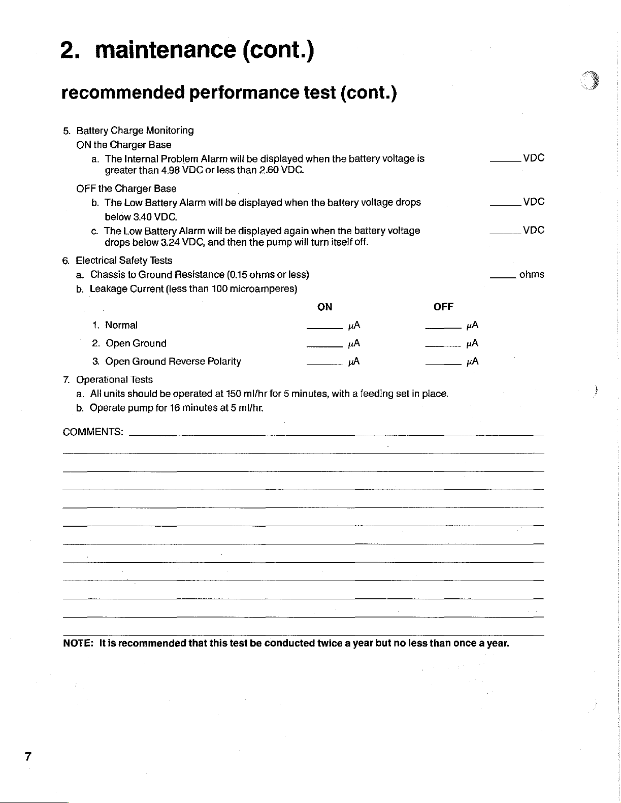
5.
Battery
ON
OFF
6.
Electrical
a.
b.
7.
Operational
a.
b.
Charge
the
Charger
a.
The
Internal
greater
the
Charger
b.
The
Low
below
c.
The
Low
drops
Safety
Chassis
Leakage
1.
2.
3.
All
Operate
to
Normal
Open Ground
Open Ground
units
should
Monitoring
Base
than
Base
Battery
3.40
VDC.
Battery
below
Tests
Ground
Current
Tests
pump
for
Problem
4.98
3.24
be
performance
Alarm
will
VDC
or
less
than
Alarm
will
be
displayed
Alarm
wili
be
displayed
VDC,
and
then
Resistance
(less
than
Reverse
operated
16
minutes
(0.15
100
microamperes)
Polarity
at
150
at 5 ml/hr.
be
displayed
2.60
the
pump
ohms
ml/hr
for 5 minutes,
VDC.
when
again
or
less)
test
when
the
when
will
turn
ON
—
(cont.)
the
battery
battery
the
itself
нА pA
pA
HA
with a feeding
voltage
voltage
battery
off.
is
drops
voltage
set
in
—
—
place.
OFF
HA
A
—
vDC
VvDC
vDC
ohms
COMMENTS:
NOTE:
It
is
recommended
that
this test
be
conducted
twice a year
but
no
less
than
once a year.
Page 11
2.
maintenance
(cont.)
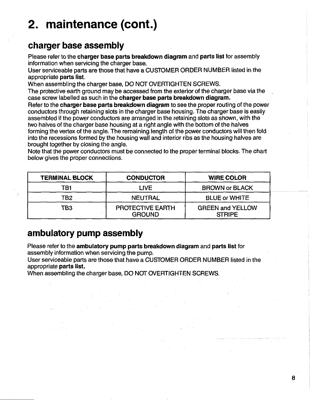
charger
Please
information
User
serviceable
appropriate
When
The
case
Refer
conductors
assembled
two
forming
into
brought
Note
below
assembling
protective
screw
to
haives
the
that
gives
TERMINAL
base
refer
to
the
when
parts
labelled
the
charger
through
if
of
the
vertex
recessions
together
the
the
earth
the
the
power
proper
TB1
TB2
TB3
power
charger
by
BLOCK
servicing
parts
list.
the
of
assembly
charger
ground
as
base
retaining
the
formed
closing
conductors
base
the
are
those
charger
may
such
in
parts
conductors
base
angle.
by
the
connections.
charger
base,
the
breakdown
slots
housing
The
the
angle.
must
parts
that
be
PROTECTIVE
breakdown
base.
have a CUSTOMER
DO
NOT
accessed
charger
in
the
are
remaining
housing
be
CONDUCTOR
base
charger
arranged
at a right
wall
connected
LIVE
NEUTRAL
GROUND
diagram
OVERTIGHTEN
from
the
exterior
parts
diagram
base
in
angle
length
and
EARTH
breakdown
to
housing.
the
retaining
with
of
the
interior
to
the
and
ORDER
see
the
the
power
ribs
proper
parts
NUMBER
SCREWS.
of
the
charger
diagram.
proper
The
charger
slots
as
bottom
conductors
as
the
housing
terminal
WIRE
BROWN
BLUE
GREEN
list
for
listed
routing
base
shown,
of
the
halves
will
blocks.
COLOR
or
BLACK
or
WHITE
and
YELLOW
STRIPE
assembly
in
the
base
via
of
the
power
is
easily
with
the
then
halves
The
are
chart
the
fold
ambulatory
Please
assembly
User
appropriate
When
refer
to
the
information
serviceable
parts
assembling
pump
ambulatory
when
paris
are
those
list.
the
charger
assembly
pump
servicing
base,
parts
the
that
have a CUSTOMER
DO
breakdown
pump.
NOT
OVERTIGHTEN
diagram
ORDER
SCREWS.
and
parts
NUMBER
list
for
listed
in
the
Page 12
3.
circuit
description
charger
AC
to
DC
Conversion
Fuses
MOV1
circuits
the
BR1
filtered
reduces
done
Supply
U2
protected
Charge
Current
connector
batteries.
Current
connector
filtered
quick
340
F1
and
and
from
115/230
is a full
by
electrolytic
an
with
C3.
Voltage
further
by
Current
regulator
J1A.
The
regulator
J1A.
by
charge
mA.
regulates
C7 and
base
F2
protect
MOV2
VAC
unregulated
large
input
wave
Output
diode
Output
U3
This
output
U4
This
the
internal
clamp
voltage
rectifier
capacitors
the
D2.
supplies a constant
is
of
supplies a constant
output
protected
the
user,
voltage
spikes
to
approximately
that
converts
:C1
DC
input
output
The
used
U3
NiCd
of
5.
VDC
by
the
is
filtered by
only
occurs
by
D4.
batteries
charging
spikes
present
and
base.
above
on
the
17
VAC,
AC
to
C2.
U1
their
pulsating
into a regulated
U1
to 5 VDC;
is
terminated
85
mA
pump
The
for
trickle
C6
and
255
mA
when
FET
combined
of
the
pump
and
rated
AC
which
pump
input.
in
voltages,
Transformer
is
fed
into
DC,
which
is a switching
7.3
VDC
output.
this
output
at
pin 2 of
fo a load
charging
protected
to a load
Q1
outputs
with a combined
is
connector
connected
by
connected
is
turned
of
then
the
D3.
U3
case
of a short
protecting
diode
is
voltage
Further
filtered
to
internal
on.
The
and U4
circuit.
internal
TX1
converts
bridge
BR1.
subsequently
regulator
that
filtering
by
C5
is
and
J1A.
pin 1 of
NiCd
to
pin 1 of
output
are
current
of
used
of
U4
to
is
%
Quick
The
no
signal
causes
allows
emitted.
connected
if
high
the
output a low signal.
LD1,
C8
output
through
control
quick
USA
pump,
(pin
regulator
current
Charge
pump
pump
generates a TTL-level
is
connected
is
high,
the
output
drain
This
or
the
control
signal
charger
at
base
extinguishing
through
of
R8.
U5B
LD1.
signal
charging
simply
3)
inverts
the
input
going
U1
required
Control
transistor
of
to
source
state
will
the
control
signal
USB
from
pin
is
powered,
The
the
After
will
then
This
cycle
from
the
is
occurring.
the
of
USA
low.
This
to
quick
to
quick
signal
to
the
charge
Q3
is
turned
this
gate
at
conduction,
last
as
long
signal
the
pump
5.
Because
the
low
output
light
output.
base
pin 4 to
allowing
as
from
the
goes
USB
combination
turns
The
about 3 seconds,
go high.
repeats
pump
output
(pins 1 and
turns
charge
charge
This
itself
is
low.
of
G3.
on
FET
current
the
The
When
2)
G1,
regulator
pump
received
or
off,
and
go high,
current
the
charger
pump
low,
pin 6 will
off
low
output
the
signal
again
as
turns
long
flashing
O3
is
high;
allowing
batteries.
by
the
if a pump
the
signal
turning
to
flow
base
is
high.
transistor
normally
of
inputs
FET
Q2
and
of
at
U5B
on
Q2
as
the
charger
of
LD1
is
turned
this
high
current
U4.
U4
charger
is
connected
at
U5B
on
through
is
powered
Q3
is
float
to
U5B
blocks
U5B
also
pin 6 will
and
is
the
on
results
to
is
then
base
pin 5 is
FET
Q2.
LD1 and
and
turned
to a high
will
cause
current
discharges
be
allows
base
current
is
visual
by a low
in
the
flow
from
able
to
at
pin 4 of
and
the
control
low.
This
This
in
turn
light
no
pump
on,
resulting
level
the
gate
flow
through
capacitor
low,
and
flow
powered
indication
input
from
output
the
supply
of
output
the
J1A.
to
in
when
the
and
that
the
U5A
of
If
low
be
is
a
to
the
Page 13
3.
circuit
description
(cont.)
ambulatory
pump
Microprocessor
Microprocessor
Motorola
groups
digit
outputs.
driven
in a 1
here)
Power
The
base.
battery
operate
and
Power
levels
MC68HC705C8
of
eight.
driver.
Ports C and D are
by
a 4
us
minimum
has
approximately 8 Kbytes
Supply
pump
The
pack
from
battery
from
are
boosted
significantly
produces a regulated 5 VDC.
connected
U13,
or
U6.
source
U13
outputs
of
power.
regulates
of
U4
Port A drives
FETs
and
MHz
can
receive
pump
contains
connects
the 5 VDC
are
prevented
the
acceptable
less
than 5 VDC.
to
J2.
The
The 5 VDC
the
U7
and
controls
8-bit
the
keypad
crystal
oscillator
instruction
power
three
to
the
output
from
here
because
output
output
output
U6
of
power
all
operations
processor
the
LED
rows,
used
for
execution
of
from
sub-C
pump
of
the
backdriving
sources
the
The
output
The
output
of
U7
of
U7
U7
down
the
drop
of
the
with
32
display
and
segments;
also
miscellaneous
that
clocks
time.
ROM
its
internal
NiCd
circuit
The
and
NiCd
cells
board
charging
each
is
fed
to
switching
input
drives
to
U2
of
U2
of
U2
the
remaining
is
also
fed
to 4 VDC.
detection
pump
I/O
and
lines
available,
charging
Port B drives
reads
the
keypad
non-bussed
the
internal
circuit
processor
144
bytes
batteries,
of
RAM
with a capacity
via
connector
base.
The
other
charging
by
diodes
voltage
is
unregulated
in
turn
drives.
is
also
used
to
pump
to
FET
Q7
to
This
voltage
circuit.
columns
1/0.
base.
divided
The
This
into
the
LED
and
processor
at 2 MHz,
(in
the
configuration
internally.
or
from
the
charger
of
J6.
1800
The
mAh.
pump
currents, 5 VDC,
D1,
D10,
and
booster
and
regulator
drive
circuit
create a switched
feeds voltage
U2.
Voltage
sometimes
U7
which
the
pump
not
driven
inverter
is
a
four
display
SW1
is
resulting
used
The
may
also
D16.
motor
by
U2,
U6;
Power-On
The
pump
Activating
from 5 VDC)
the
microprocessor
the
processor
U9
and
controls
power
because
latch
be
the
pump
The
circuit
generated
microprocessor,
microprocessor
been
the
latch
latch
will
is
turn
Circuit
circuit
this
normally
that
turns
Q4
and
FET
Q18.
from
all
U9
is a CMOS
and
by
circuit.
pressed,
because
is
disabled.
disabled, a RESET
on.
The
microprocessor
purpose
of
this
may
be
activated
open
is
connected
is
already
on
the
rest
the
resistors
Q18
lies
in
pump.
circuits
IC. A negative
©18
if
not
already
the
regulators
turning
also
it
monitors
constant
If
the
pump
pulse
microprocessor
will
turn
on
and
arrangement
in
switch
powered
and
the
except
creates a negative
to
the
IRQ
of
the
capacitors
main
for
turned
and a pulse
on.
The
/O
current
is
connected
will
be
will
not
only
activate
is
to
enable
two
ways.
line
when
pump
The
of
the
this
occurs,
circuit
if
connected
ground
the
going
latch,
pulse
on.
If
will
path,
which
from
the
latch
be
generated
microprocessor
line
PC1.
regulator
generated
see a low
the
PC1
Q10
to
an
as
on
timing
processes
microprocessor
first
is
by
pressing
going
pulse
(dropping
microprocessor
an
interrupt
not
already
to
them
and
is
draws
the
and
will
then
will
only be low
keeps
active
charger
above,
PC1
however,
turned
form a latch
used
to
negligible
ON
key
Q18
turn
to
the
turn
C45
charged
base
and
the
in
the
to
start.
the
ON
to
and
to
U9
pin
is
generated
on.
that
completely
power
will
turn
on,
RESET
on
the
if
the
on
power
input
rest
ON
key
remove
of
even
while
the
microprocessor
so
the
software.
quick
The
charging
key.
ground
2.
If
and
the
will
of
the
has
when
the
10
Page 14
3.
pump
was
Removal
circuit
battery
not
activated
of
power
accomplished
power
to
all
circuits
description
as
soon
and
to
by
asserting
as
the
the
ON
the
microprocessor
port
except
for
pump
switch
PCO.
Q10
is
plugged
was
This
and
(cont.)
into
the
not
pushed.
and
the
rest
turns
U9.
off
the
charger
of
the
latch
base,
pump
and
even
circuits
FET
Q18,
if
the
is
killing
latch
ED
v
Reset
The
as
result
U12
pulse
constantly
U12
will
isolate
Battery
Resistors
Circuit
microprocessor
seen
earlier,
in a pulse
is a watchdog
every
250
reset,
also
monitors
generate a reset
U12
power
Monitoring
R5
and
A/D converter
bits
are
read
serially
milliseconds
Software
quick
U11)
Touch
The
charging
to
deliver
Panel
touch
arranged
PB3.
Microprocessor
microprocessor
represent
not
part
this
switch
displayed
lines
from
(or
in
the
panel
in a 3x3
each
of
the
is
driven
on
the
each
may
is
the
generated
timer
milliseconds.
U12
its
from
R6
into
an
every
receive a low
activation
by
and
power
will
generate a pulse
supply
pulse
divide
eight
by
other
voltage.
to
the
the 5 VDC
the
bit
the
microprocessor
resetting
microprocessor
is
necessary,
quick
charge
is
connected
matrix,
ports
decodes
switch
matrix.
Microprocessor
by
LEDs.
other.
Switch
in
PBO.
port
current.
with
PB4,
the
row/column
the
matrix.
Switch
Diodes
input
of
the
latch
circuit.
R12
and
C11.
monitor.
This
pulse
train
at
If
its
supply
microprocessor.
buss.
battery
voltage
representation
using
of
the
watchdog
determines
PC5
to
the
pump
the
rows
PB5
and
It
should
SW1
D4A,
D4B,
debouncing
when
signals
circuit
being
PB6
information
ports
is
used
PB4,
D18A, D18B,
is
on
the
RESET
Power
The
microprocessor
resets a timer
its
output
drops
Diode
by
2;
of
one
ports
the
the
charger
board
driven
read
the
be
noted
PB5
to
select
applied
which
below
D9 and
this
voltage
half
of
PC7,
timer
battery
with
by
microprocessor
column
and
that
and
the
D12,
accomplished
line
for
three
to
the
reasons.
pump
generates a negative
in
U12.
If
this
timer
will
reset
the
microprocessor.
approximately
capacitor
is
then
the
battery
PC6,
U12).
needs
base
(isolated
connector
voltage.
and
to
be
4.5
C43
converted
PDO
every
quick
by
optoisolator
J5.
The
ports
information.
generates a unique
the
ON
key
PB6
also
read
language
D13A
in
and
software.
Software
is
independent
switch
for
messages
D13B
isolate
The
circuit
is
not
VDC,
somewhat
by
The
eight
500
charged.
panel
PB1,
PB2
byte
to
SW1
parallel
first,
will
going
U12
the
If
is
and
in
the
and
when
.
Så
11
LED
Display
LEDs
messages.
Q13
DP4,
DP3,
Microprocessor
respectively.
connections
by
port A of
drive
the
the
display
DP2
and
DP1
The
FETs
than
possible
with
microprocessor.
segments.
are
used
to
ports
PB3,
PB2,
allow a greater
the
microprocessor
These
I/O
display
PB1
current
lines
feeding
and
flow
are
profile
PBO
drive
to
the
I/O
ports.
capable
information
FETs
LED
segment
Segment
of
sinking
and
Q16,
Q15,
Q14
common
information
enough
current
error
and
is
driven
to
Page 15
3.
Drop
The
Two
through
photodiode
drip
through a sixth
to
surrounding
then
circuit
Detector
pump
IR
chamber
the
monitors
LEDs
are
J3
pins 3 and
is
protected
yoke.
order
microprocessor.
passive
input
to
the
Motor
The
pump
is
controlled
on
simultaneously,
motor
by
microprocessor
surrounding
before
applying
removed
RC
before
Fail-Safe
In
the
unlikely
circuit
Q3
the
Q2
O1
F1.
will
gets
voltage
turns
turns
The
its
fail-safe
event
crowbar
power
at
the
on,
raising
on
and
description
fluid
flow
by
optically
driven
microprocessor.
is
FET
controls
networks.
power
applying
from
anode
allows
circuit
by
constant
4. A photodiode
from
the
The
signal
low-pass
The
networks.
connected
Q6.
The
and
are
the
through
from
filter,
signal
The
to
motor
time
motor
The
RC
Q6;
dynamic
that
the
motor
the
power
the
the
current
takes
supply
motor
of
Q2
exceeds
voltage
from
approximately
effects
from
the
delayed
circuit;
at
the
(cont.)
detecting
current
the
amplified,
output
pump
is
also
from
networks cause
conversely,
brake
should
to
gate
the
source
is
likewise
of
visible
photodiode
chopped
the
photodiode
of
this
circuit
braked
so
that
they
port
TCMP.
power
Q5.
continuously
ground
as
the
battery
and
the
motor
voltage
of
Q1.
to
13
seconds
connected
processing
When
drops
Q11
failing
and
connected
to
light
by a polysulfone
is
amplified,
and
finally
is
processed
is
board
by
pass
FET
never
This
the
dynamic
to
run
blow
runs,
on
the
directly
to
by
connector
Q5.
Q6
transition
signal
the
motor
and
fuse
Fi.
Q3
gate
the
gate
trip.
through
J3
pins 1 and
differentiated,
then
and
the
to
the
filter
squared
by
U5
and
buffered
J2.
Power
Q5
are
integral
for
simultaneously.
is
buffered
brake
through
not
turn
Constant
charges
(set
by
of
Q1
through
by
O5
to
Q6
off, a fail-safe
current
capacitor
divider
rises
above
it
to
ground,
drip
chamber.
circuit
2.
board
The
to
passed
the
presentation
the
by U1
never
and
to
the
turned
motor
The
U1
and
the
be
released
is
always
regulator
C3.
When
R1
and
R2),
ground,
blowing
Rotor
The
the
Detection
microprocessor
interaction
of 3 magnets
microprocessor
in
software.
Frame
The
effect
pocket
Pump
The
switch
the
arm
Audio
Audible
board
port
Detection
microprocessor
switch
Set
microprocessor
S2. A magnet
in
the
frame.
Detection
connected
pump
set
and
the
Alarm
alarms
through
PC3
is
activates
loading
connector
boosted
monitors
receives
detects
detects
to
the
the
arm
are
generated
by
U14
the
in
pump
switch
is
then
J4.
and U15
the
rotation
on
the
signal
the
presence
the
frame
the
presence
circuit
when
pump
from
of
rotor
S1
of
will
of a pump
board
the
the
with
on
port
the
close S2
through
pump
closed.
using a piezoelectric
The
TTL-level
to a
oscillation
20
VDC
.
DC
motor
Hall-effect
PD5.
Debouncing
backpack
when
set
on
J1
pins
set
is
properly
element
generated
level.
by
counting
switch
frame
the
pump
port
on
PD7,
4, 5 and
inserted
connected
by
pulses
S1.
of
port
is
fully
using a Hall-effect
6.
The
to
the
microprocessor
The
this
switch
PD3,
inserted
SIPS
into
the
the
pump
generated
occurs
using
Hall-
into
magnet
loading
circuit
by
its
on
at
12
Page 16
3.
circuit
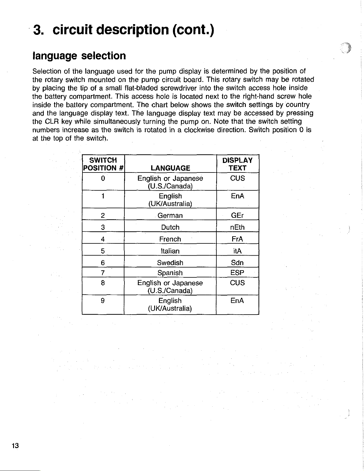
language
description
selection
(cont.)
Sage”
E
Selection
the
rotary
by
placing
the
battery
the
CLR
the
the
language
key
top
inside
and
the
numbers
at
of
the
language
switch
the
compartment.
battery
increase
of
mounted
tip
of a small
compartment.
display
while
the
simultaneously
as
switch.
SWITCH
POSITION
the
0
1
2
3
4
5
6
7
8
9
used
for
the
pump
on
the
pump
flat-bladed
This
access
The
text.
The
switch
is
#
English
English
screwdriver
hole
chart
language
turning
rotated
LANGUAGE
(U.S./Canada)
English
(UK/Australia)
German
French
Halian
Swedish
Spanish
(U.S./Canada)
English
(UK/Australia)
display
circuit
or
Dutch
or
board.
is
located
below
the
in a clockwise
Japanese
Japanese
shows
display
pump
is
determined
This
into
the
next
to
the
text
may
on.
Note
direction.
rotary
DISPLAY
switch
switch
the
right-hand
switch
be
accessed
that
the
TEXT
CUS
EnA
GEr
nEth
FrA
itA
Sdn
ESP
CUS
EnA
by
the
position
may
access
settings
Switch
hole
switch
position 0 is
be
rotated
inside
screw
by
country
by
pressing
setting
of
hole
Page 17
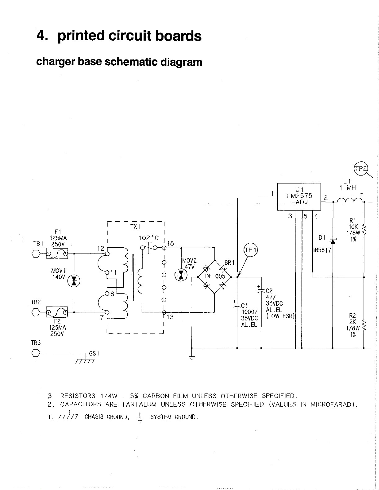
4.
printed
circuit
boards
charger
125MA
ТВТ
OR
250v
Fİ
base
schematic
diagram
fP
1
|
U1
LM2575
—ADJ
3|
Isla
IN5817
2
D1
L1
1
MH
一 一 一
^
Ri
10K
1/8W
M
i
MOV!
Мо
182
125MA
250V
TB3
THE
3.
2.
1.
р)
RESISTORS
CAPACITORS
77777
CHASIS
1/4W
ARE
GROUND,
,
5%
CARBON
TANTALUM
Å
UNLESS
SYSTEM
=
FILM
UNLESS
OTHERWISE
GROUND.
BRI
Le
АЕ.
OTHERWISE
SPECIFIED
ce
47/
35VDC
ЕЕ
SPECIFIED.
{VALUES
IN
MICROFARAD).
ew
=
1%
Page 18

Page 19

uz
RS
1/8W
1%
[66100
μη
77907
000
U3
=>)
N
[171086
iL)
一
——
TFT
|
(H3)
一
—
1086]
IN
|!
OUT A vis
|
十
一
十
out
oyn
OUT
Jl
3
L
L
=
22/
10006
»
Co
ee
10VDC
2N3906
1
CER
R4
izin
1/8W
1%
ce
03
((P9)
RE
бо | INS817
RT
ato
了
R10
49.9K
VEN
Da
(РЭ
οἱ
|
i
|
Œ
;
i
|
!
1
i
i
τῷ
|
1000/
|
16006
AL.EL
if
|
(LOW
| 1
LD1
HLMP
1520
R3
1202
ESR)
LE
]
Lio
9123
+
|
3
À
2
A,
|
uz
|
CS
100/
10vDc
D3
时
4
{
1N5817
R9
12K
|
RU
WW
2.2K
ei
ペーー
JIA
STANDARD/QUICK
CHARGE
REGULATED
GROUND
STANDARD
ト
CHAR6E
/QUICK
CONTROL]
|
7
5
5)
バジ
Page 20

Page 21

charger
base
PCB
assembly
TP4
ar
р
LI
E
Cg
diagram
Fa
i
Ú3(
OLD1
U4
UUU
MEDICAL
CHARGING
BASE
UNIT
ce(
GS1
|)
ВВ!
一
7p3
C7
C1
一
α΄
SECONDARY
一
©
=
©
|
ra
2
Μον2
TP7
LU
|
D4
|P
C3
ma
a3<
|
Ra
92
R11
4
UNU
Ro]
J
4
1
b2
[70
—
ППП
Lol?
1A
©
pee
レー
N_
C5
$
115
1181
C
220
- =
PRIMARY
PA
-
115
Cemi
TX1
LO
dk
00593
00595
REV
Γ
Fe
===
TB3
TB2
El
ノ
Page 22

Page 23

parts
list
REORDER
7774101682
7774-101955
7774102003
-
7714102029
7774102060
7774102078
7774-200427
7774-202563
7774-202571
7774-300441
7774-300466
7774-300730
7774-030089
7774-030865
7774-030006
7714-030014
7774-400753
7774-040104
7774-401611
7774-402684
7774-402866
7774-404144
7774-040427
7774-406248
7774-406586
7774-406594
7774-406602
7774-500818
7774-050186
7774-501717
7774-501733
7774-501741
7774-501766
7774-501899
7774-600618
7774-802669
7774-802776
7774-400613
7774-302785
7774-310457
NOT
AVAILABLE
7774-802974
7774-501725
NO.
FUSE
CLIP
18
AMP
1MH
INDUCTOR
HEAT
SINK
HEAT
SINK
TRANSFORMER
QUAD
1.5A
LOW
STEP-DOWN
MOSFET
PNP
TRANSISTOR
SCHOTTKY
HEXFET
140
VOLT
BRIDGE
47
VOLT
49.9K
OHMS
120
OHMS
12K
OHMS
2K
OHMS
2.2K
OHMS
10K
OHMS
330
OHMS
383
OHMS
121
OHMS
15
OHMS
4.7
OHMS
10
UF
SOLID
100
UF
47
UF
AL.
100
UF
22
UF
SOLID
1000
UF
0.1
UF
GREEN
4
PIN
FRICTION
TERMINAL
NO.
4-40
NO.
4-40 x %
CHARGER
| THERMAL
TEST
PIN
1000
UF
DESCRIPTION
FAST
ACTING
NAND
CERAMIC
4093
DROPOUT
VOLTAGE
TRANSISTOR
DIODE
TRANSISTOR
VARISTOR
RECTIFIER
VARISTOR
4W
%W
5%
%4W
5%
WW
1%
Ya W 5%
74W
1%
WW
5%
14W
1%
14W
1%
%4W
5%
%4W
5%
TANTALUM
SOLID
AL.
TANTALUM
ELECTROLYTIC
ELCTROLYTIC
TANTALUM
ELECTROLYTIC
CAPACITOR
LED
T-1
UNTINTED
LOCK
BLOCK
KEP
NUT
PAN
GROUND
JOINT
AL.
ELECTROLYTIC
FUSE
115/230
1%
RESISTOR
RESISTOR
COMPOUND
VAC
POS.
REGULATOR
REGULATOR
IRFD9123
2N3906
1N5817
123
RESISTOR
RESISTOR
RESISTOR
RESISTOR
RESISTOR
RESISTOR
RESISTOR
RESISTOR
RESISTOR
CAPACITOR
CAPACITOR
CAPACITOR
CAPACITOR
CAPACITOR
CAPACITOR
HEADER
HEAD. X REC.
STRAP
CAPACITOR
QTY
4
__|
2 | Fi,
1
2 | USEDWITMU3,U4
1
1
1
3 | U2,
1
1
1
4 | Di,
1
1
1
1
1
1
1
1
1
1
1
1
1
1
1
1
i
1
1
2 | С6,
1
1
1
1 | JIA
3 | TB1,TB2,
3_ | USED
3. | USED
1
AR | USED
1
DESIGNATION
USED
F2
11
USED
(TX
US
U3,
ui
οἱ
|Q3
D2,
02
MOVI
BRI
MOV2
Rio
АЗ
Rg
R2
ATİ
RI
R8
RS
R4
R6
R7
C8
C5
C2
C4
С7
C1
C9
LDI
GS1
TP1
C3
WITH
WITH
U4
D3,
TB3
WITH
WITH
WITH
F1,
U2
D4
U2,
U2,
U2,
F2
U3,
U3,
U3,
U4
U4
U4
}
15
Page 24

Page 25

4.
printed
circuit
boards
(cont.)
pump
schematic
τι
R56
1000
R26
100K
diagram
>
1/8W
1
LI
47
U2
LT1110CS8
6]
8]
475
|
|
T6
UH
D2
1N58
18
T2
R27
as
2|
T10
SPT
от
yi
11
sel
T11
O
?
—
|!
|
|
ヒーーー
—
PAD
©
©
PICK-UP
7
Ll
|
|
FOR
TERMINAL
a
WIRE
SOLDERING
OUT
8
1
049
4.7UF
16VDC
TANT
U15
CD40
|
|
で
—
14
106BM
7
]
3
ン
i
o
IN
R39
10K
LT
>
U14
1026C%
3
Ll
LE
T-
046
Е
4
16VDC
TANT
M
|
MODULAR
SCHEMATIC
Page 26

Page 27

97
TP0602N3
D
G
s
73
4.7UF
16VDC
TANT
+)
+
4.
16VDC
TANT
C47
¢
C
(
6
048
7UF
14
3}
шв
PS2505-1
051
10UF
10VDC
TANT
I
TI
>
©
Г
|4
16
Page 28

Page 29

4.
printed
circuit
boards
(cont.)
pump
в
A
MALE
AND
HOUSING
시
a!
[
it
ita: t +
ELT
P
BLACK
PES
Ear
уж. | (©)
so.
ge
Sana.
1. 7 SEGMENT
2.
UNLESS
ALL
ALL
ELECTROLITIC
CAPACITOR
3,
GROUND
4...
„A
MIRE
7
BAM
TP
5 3
\
Y
ou
O
\
asa
Jr
|(G
Apa
cer
Tie
СЫ
i
1
|
!
A-
©
©
©
©
OTHERWISE
RESISTORS
CAPACITORS
SYMBOLS:
REQUIRES
schematic
TERMINALS
(21
때
BAT
q
(+)
o
pte
MBRS
k
de
MIER
Bi
MORS
7
tox | Barra M T
“o
DC
δι
TO
04
>
ΤΡΙ
ΞΒΙΤΕΝ
TP3 = OLIVE
PS = BACK-PACK
TP7 = v
TP9 = DIG
TEN = MOT Y TPII
Ta =v
TP15 = WATCH
TP17
=
FILTER
TP
19 = LO_BAT
‘Tat = -av
TP23
=
CHRG CONT
TP25 = (.R
LED
DIGITS
SPECIFIED:
1/10W 5 PCT
MONOLITHIC
CAPACITORS
VALUES
IN
SHORTEST
7
-75A
je
+
À
os
.-.
fn
TEST
PAD
REG
GND
TP13
DOG
OUT
TPIT
TP19
CUR
TO
BE
CERAMIC
ALUMINUM
MICROFARADS.
W
ANALOG:
AND
VBAT
=
NL
SHOWN
TPI
me
Tea
TPS
구오
TI
0:
189
00-
TPIS
ZE
=ю
TP21
00
ТРЗ
Ol
TP25
Qi
INSTALLED
METAL
THICKEST POSSIBLE
diagram
RI
ag
в
οι
Re
JA
MCR る 178K
ти
KİNE
si,
ROTATED
90“
VS
ーー
poste
FILM
Y
PCB
tê
TP4
Te
Te
TPIO
ТЫ
TPM
¡O
TP16
TPI
Po
TPzz
1824
1026 TP26 = DEAD
WITH
DECIMAL
DIGITAL: 1 SWITCHED
tray
6.
이
DWG.
TRACE.
4
|
1
R3
šk
so
кот
i
i
vB
POINTS
os
LM334M
30-8
a
2N6028
Ra
İK
w
ri
:
|
:
L
ma
38716V
1
è
BAT
AT
TOP
LEFT
SYSTEM
RIT
™
1.5K
1/8
CORNER.
GROUND.
ML
si
トー
R38
OHM
W.
D5
BATIA,
|
Artes
Ê
1%
г
이
이언
elio;
101
TACT
(50-14)
이 나 el
cz
47
52
R52
2.2K
주
:
=
5%
D7
MMBDS
14 E
ot
=
Rzs
13)
14D
14
η
05
$35
이
R24
took
yz
la
l+
1007
*
==
al
3
4fpsz505-1/2
4
I Е Y
ps
站
65-
ую
io
-本 一 一
A
가
rae
100/10V
05
IRFD123
s
5
G
De
entro
1
1
HH
wz.
TANT
@
TANT
o-
2
2
BE)
Е
ca7/+
1007
(5)
©
Ge
TPOB02N3
ce
wl
1
>
ro
る
200K
s 4
U7
fLri1z0
주 | ons
(m
TRI
1.9
Me
3%
RO
SK
© ©
[8]
Geek
ÍTANT
жена
POWER
Ton
pes
Aso.
000.
MES
5
VT
=
aa.
Riz
VBAT
DI
RB400D
6.swvpc し ヨ
Ls
LE
ασ
A
ue
MAX
1232
8
6
7 F
20K
Z
πο
4.77100
+4V
o!
el
2p
T
100/10
TANT
3
ON
LATCH
costo.
BATI,
HOOK-UP
EE
7
'
Re
100K
08
|prettan
2
|
f
>
É
ь:
2
<
pd
Page 30

Page 31

]
l
og
:
E
|
RU
|
+
Ld
4
1
2
£
é
4
1|38|36
Poo
Po7
ecs
RESET
pee
Poo
pps
бы
poz
MV
トー
Y
jas
ВЕН
Е
>
ΜΟΡΘΗΟΤΟΡΟΘΕΝ
44
5
っ a
5
8
2
2
[22
43
RIS
2.2MEG
166
pa
MMBDS
cs
107
tov
TANT
it
ルー]
1
016
R43
100K
i
vy
Ja
Po er
E
>
va
LEAD PLCC
은
은
41
|
=!
4
14)
Y
vu
NZC
ci?
|
2.
-
1
у
la
à
BE
38
à
3
E
9
us
LMF60CWM
-100
tso-14)
e
Jı
İs
5
AAA
|16|15
14119
ава
a
aaa
P86L20
685|
P84[
mes
Lao
Paol12p
PAI
paz
[ιδιο
도모
paola
РАЗ
pns 上 y
ra
РАТЬ
30
pci
PD3
PDI
33
RS232
|
Why
usa
Ма
В.
ROS
9.1K
4
19 _ 4
4
17
+25)
Rs | do
주니
=
91
E
RAS
it
pe
pu
13
№
мл
Lia
2001-
48169700
OHM
750
—
17
ГВ
14
la
に
1-751
18)
NE
τρ
1
di
GRATE
bras
|
||
цу
Ом
8
6
-1
İz
pk
の
5
ЕВЕ
13
a
T3
cas
TANT
piz|
LA
15%
[4
1
b
2
5
5
5
4
3
2
i
o
i
14|3
P|
D13
|
+4V
8
06
TOS962CPA
m
CAN
f
N
V
saimos
1
+
sz
ЗАРЕ
-
3
013
—,
deb
я
Fi
on
ol
的
v
7.54
DIGIT
5
AH)
625
리너
3
Us
|
7
6
4
а
1
Jia
wolf
5
100/10v
TANT
say
915.16
zf
5
es
ñ
η
5
{ops
一
|
一
|
GS3
Xq
3
о
|
T
614 T gl
2
s)
|
|
|
ihh
в
pp4
一 | 一
ГИГИЕНЕ!
一
一
PS4
SD
N
C44
Aloe
TANT
eo
A
016
al,
5
T
」
|
D
,
y
TPOBOENS
joe
fort
一 | 一
一
|
一
—
|
一
CS1
DSz
0050}
i
ci
l
[cis
Tezer
У
RS232
17
Page 32

Page 33

4.
printed
circuit
boards
(cont.)
pump
PCB
assembly
diagram
BLACK
{-}
COMPONENT
SIDE
Page 34

Page 35

İPİN
1
COMPONENT
SIDE
DETAIL
一
655
이그
Я
oe"
R41
日
Π
R40
61000
00
a
R47
R34
SOLDER
ロロ
035
RIS
只
Does
cio
652
SIDE
=
5
τα
026
o
o
o
ο
o
a
ο
o
o
8
o
o
£
Page 36

Page 37

5.
final
assembly
charger
base
parts
breakdown
diagram
Page 38

Page 39

a
El
т
©)
\
WIRE
ROUTING
DETAIL
a
EARTH
ACCESS
GROUND
19
Page 40

Page 41

5.
final
assembly
(cont.)
pump
parts
breakdown
diagram
Page 42

Page 43

5.
final
assembly
charger
ITEM
1
4
10
11
12
13
14
15
16
17
18
19
20
21
22
23
24
25
26
27
28
29
30
31
32
33
34
34B
34C
34D
ЗАЕ
34G
36
37
34F
38
*PART
OF
ITEM
base
REORDER
7774-005933
7774-905934
7774-903889
7774-809516
7774-808625
7774-303213
7774-304849
7774-304864
7774-304948
7774-305002
7774-305010
7774-402429
7774-500131
NOT
7774-807528
7774-807932
7774-309996
7774-310028
7774-310036
7774-310044
7774-310051
7774406327
7774-310499
7774-311034
7774-310788
7774157924
7774-090026
34
(7774-311034)
parts
NO.
7774-154111
AVAILABLE
7774-181007
7774-310010
7774-310127
*
*
*
3
*
*
list
CHARGER
CHARGER
POWER
FUSE
GROUNDING
MYLAR
NO.
NO.
NO.
NO.
STRAIN
NO.
POLE
PERMANENT
DOW
WRITE-ON
SERIAL
FUSE
COUNTERSUNK
POLE
POLE
SLIDELATCH
POLE
BACK
CHARGER
POLE
FRONT
EXTERNAL
ANESTHETICS
DIRECTION
RELEASE
CHARGE
CAUTION
CABLEWRAP
GROUND
WARNING
Ys”
CORD
WARNING
OVERLABEL
4-10 x 4"
6-32 x 1”
4-10 x 46”
2-56 x 2"
RELIEF
4-40 x 4%"
CLAMP
CORNING
NUMBER
REPLACEMENT
CLAMP
CLAMP
CLAMP
SHELL
CLAMP
SHELL
DIA,
PCB
ASSEMBLY
PCB
ASSEMBLY
LABEL
LABEL
SELF-TAPPING
MACHINE
FLAT
HEAD
ELAT
HEAD
FLAT
HEAD
BUMPER
EASTENER
738
ELECTRICAL
LABEL
LABEL
LABEL
WASHER
SCREW
KNOB
CONNECTOR/WIRE
SPRING
ASSEMBLY
CHARGER
LABEL
FOR
USE
LABEL
LATCH
LABEL
ACTIVE
SHOCK
LABEL
SHRINK TUBING
LABEL
HAZARD
LABEL
SCREW
LABELS
DESCRIPTION
(BOARD
SCREW
SCREW,
SCREW
CAP
SCREW
SEALANT
ASSEMBLY
LABEL
EXCHANGE)
QTY
1
1
1
1
1
2
5
2
2
1
1
1
1
AR
1
1
1
1
1
1
1
1
1
1
1
1
1
*
*
*
*
È
1
1
1
AR
20
Page 44

LE
제
Page 45

21
Page 46

Page 47

5.
final
assembly
(cont.)
pump
ITEM
29
30
31
32
33
34
35
36
37
38
39
42
43
44
45
46
47
48
49
51
52
53
54
55
56
57
58
59
parts
1
2
3
4
7
8
list
REORDER
7774-005925
7774-905926
7774405691
7774-106350
7774-106335
7774-701085
777440634
7774-809516
7774-808120
7774-178003
7774-303213
7774-304849
7774-304898
7774-304906
7774-304914
7774-304948
7774-402460
7774-500016
NOT
AVAILABLE
NOT
AVAILABLE
7774-809987
7774-807528
7774-807536
7774-807551
7774-807890
7774-106368
7774-309798
7774-309806
7774-106376
7774-309830
7774-309848
7774-309863
7774-309871
7774-310135
7774-310465
NO.
PUMP
PCB
ASSEMBLY
PUMP
PCB
ASSEMBLY
BATTERY
SWITCH
MOTOR
TOUCH
PUMP
FUSE
CHARGE
MYLAR
NO.
NO.
NO.
M2x5
NO.
NO.
QUAD
MINIATURE
DOW
DOW CORNING 7 RELEASE
SERIAL
WRITE-ON
FULL
FUSE
BATTERY
BUZZER
CONNECTOR
LOADING
YOKE
FRONT
BACK
SHIELD
BATTERY
LOADING
ROTOR
PACK
ASSEMBLY
ASSEMBLY
PANEL
CONNECTOR/WIRE
WARNING
REQUIREMENT
OVERLABEL
4-10 x Ya”
6-32 x 1”
6-32 x %"
METRIC
4-10 x 3%”
2-56 x V2“
RING
CORNING
LINE
REPLACEMENT
ASSEMBLY
CASE
SELF-TAPPING
MACHINE
FLAT
FLAT
SELF-TAPPING
FLAT
CABLE
NUMBER
LABEL
LABEL
WARNING
ASSEMBLY
CLAMP
ARM
CASE
COVER
ARM
ASSEMBLY
LATCH
LATCH
ASSEMBLY
LABEL
HEAD
HEAD
HEAD
TIE
738
ELECTRICAL
LABEL
LABEL
LABEL
SCREW.
DESCRIPTION
(BOARD
SCREWS
EXCHANGE)
ASSEMBLY
LABEL
SCREW
SCREW
SCREW
SCREW
SCREW,
COMPOUND
SEALANT
QTY
1
1
1
1
1
1
1
1
1
3
5
2
3
2
2
1
5
AR
AR
1
1
1
1
1
1
1
1
1
1
1
1
1
1
Page 48

Page 49

ITEM
60
61
62
63
63A
63B
63C
63D
*PART
OF
ITEM
REORDER
7774-310507
7774-310515
7774-310523
1774-310473
63
(7774-310473)
*
*
+
*
NO.
MOTOR
LOADING ARM
LOADING ARM
EXTERNAL
RECYCLE
LOADING ARM
ALARM
ALARMS
SLEEVE
TEST
LABEL
PUMP
LABEL
LABEL
ASSEMBLY
LATCH
SPRING
ASSEMBLY
LABELS
RELEASE
DESCRIPTION
LABEL
QTY
1
1
1
1
*
*
*
*
22
Page 50

Page 51

6.
Type
specifications
Infusion
Volumetric
Device
Pumping
Rotary
Pump
Set
Sherwood
Operating
Rate
1-75
75-400
Dose
1-75
75-2000
Interval
1-24
Volume
1-9999
Accuracy
+/—
10%
Occlusion
12
psi
(82.7
15
psi
(103
Mechanism
Peristaltic
Required
Medical
Range
mi/hr
in 1 mi/hr
mi/hr
in 5 mi/hr
ml
in 1 ml
ml
hours
Delivered
ml
of
Pressure
kPa)
increments
in 5 ml
in 1 hour
selected
kPa)
Nominal
Maximum
Kangaroo
increments
increments
increments
increments
flow
rate
Feeding
Pump
Administration
Sets.
Alarms
Internal
No
System
Low
Flow
Dose
Hold
Circuit
Set
Alarm
Error
Battery
Error
Delivered
Error
Battery
Rechargeable
Automatically
Recharge
discharged
A
new
battery,
Dimensions
Pump:
Pump
with
Problem
Alarm
Alarm
Alarm
Alarm
Alarm
NiCd
charges
time
for
fully
batteries
when
Charger:
Alarm
1800
mAh
when
will
fully
5.75"H x 3.81” W x
6.25"H x 4.50”W x 4.60”D
pump
discharged
take
less
time
charged,
is
placed
battery
to
fully
will
operate
2.00"D
on
is
approximately 6 hours
charging
charge
for
approximately
(14.61 x 9.68 x 5.08
(15.88 x 11.43 x 11.68
base
(minimum
connected
maximum.
45
minutes).
14
hours
cm)
cm)
to
at
wall
125
outlet.
Partially
mi/hr.
23
Page 52

6.
Weight
Pump:
Charger
specifications
Approximately
Base:
Approximately
(cont.)
1.4
Ib
2.08
(635
Ib
(944
#3
9)
g)
Case
Power
Material
ABS
Plastic-FLAME
Requirements
120
VAC,
220-240
Chassis
to
Leakage
Memory
16
Operating
50°
40°
Transport
32°
Accessories
The
Kangaroo
Kangaroo
of
hours
to
105° F (10°
to
105° F (5°
and
to
122° F (0°
Kangaroo
50/60
VAC,
Current
Settings
for
Temperature
Hz, 1 Amp-North
50
Hz,
Ground
Resistance
<=
when
all
settings
to
to
40°
Storage
to
50°
Pet
enteral
Pet
Feeding
Pet
Carrying
RETARDANT
0.5
Amp-Europe,
100pA
Pump
40°
C)
If
Charging
C)
If
NOT
Temperature
C)
feeding
Pump
Case
with
with
America,
<=
0.15
is
OFF
Charging
system
Charger
Frame
Japan,
Australia
ohms
-
consists
Base
8884-350409
Hong
of:
8884-350003
Kong
Kangaroo
The
Kangaroo
Pet
Charging
Pet
Feeding
Cable
Pump
8884-350490
is
to
be
used
only
with
Kangaroo
Pump
Sets.
24
Page 53

7.
troubleshooting
guide
Listed
their
Alarm
Alarm
below
corrections.
Symptom ; Probable
No
Set
(no
SEt) | placed
Flow
Error | Feeding
(FLO
Err) | empty.
are
Pump
been
pump.
container
Feeding
feeding
tubing
occluded.
Drip
chamber
walls
with
feeding
formula.
Sensor
drip
chamber
guide
some
improperly | has
are
is
of
the
probable
Cause | Corrections
set
has
onto
is
tube
set
is
coated | detector
in
upper | Check
blocked. | by
Check
Check
properly
Refill
in
use
or | Locate
may
©
Feeding
*
Feeding
*
Feeding
obstruction.
Check
be
removed
chamber
guide
using a cotton
water
to
make
been
placed
to
make
positioned
feeding
for
24
point
occur
upstream
Container
Pump
Tube—feeding
to
make
from
manipulation,
to
make
is
free
or
isopropyl
causes
sure
that
onto
sure
that
on
container.
hours,
of
from
of
replace.
occlusion
Set
sure
formula
proper
inside
sure
black
dried
swab
alcohol.
operation.
formula.
of
alarm
only
the
the
the
if
or
downstream
(control
walls
replace feeding
dampened
conditions
Kangaroo
pump.
pump
pump.
feeding
and
correct.
clamp
tube
should
is
not
if
of
chamber
surface
Remove
Pump
set
has
been
set
has
been
Note:
from
pump.
closed)
be
checked
preventing
formula
of
with
set.
drip
any
warm
cannot
via
chamber
deposits
and
Set
occlusion
for
drop
soapy
Low
Battery
Alarm
(LO
bAt)
Hold
Error | Pump
Alarm
(HLd
Err) | mode
System
Error
Alarm
(SYS
Err) | or
Internal
Circuit
Problem
Alarm
(8888)
Dose
Delivered | been
Alarm
(dOSE
dEL)
Battery has
run
down.
left
in
25
minutes.
Problem
rotor,
position
other
circuit
Problem
internal
circuitry.
Preset
to
patient.
been | Insert
has
been | Press
the
hold
for
over
with
rotor
sensing
rotor
problem.
with
pump
dose
has | Repeat
delivered
pump
into
charger
into
wall
outlet.
START/HOLD
START/HOLD
and
press
Return
Return
delivered;
DOSE
increase
A
pump
pump
and
until
new
the
START
dose
OR
CLR;
the
dose
again
for
technical
for
technical
-
amount
cancel
OR
dose
amount
is
/HOLD
base
to
silence
to
restore
again
service.
service.
by
clearing
the
dose
to
feed
additional
by
pressing
displayed;
and
plug
alarm,
then
flashing
to
restart
the
feature
OR
by
turn
power
press
rate
display,
pump.
volume
pressing
volume,
DOSE,
the
pump
cord
then
off.
25
Page 54

8.
A.
factory
Inthe
1.
Call
instructions.
2.
Pack
event
that
Customer
the
instrument
service/ordering
it
is
necessary
Service
carefully
at
to
(800)
and
return a unit
448-0190
ship
for
to:
for
repair,
Authorized
information
please
Return
observe
Number
the
following:
and
shipping
B.
To
place
(800)
an
order
448-0190.
for
repair
parts
Sherwood
98.6
Faichney
Watertown,
or
if
technical
Medical
Drive
NY
13601
assistance
Co.
is
required,
call
3
È
A
26
Page 55

Page 56

181038
H-122-92
Printed
©1993
in
U.S.A.
SHERWOOD
MEDICAL
COMPANY
A
Sherwood
MEDICAL.
ST.
LOUIS,
MO,
63103
U.S.A.
Se
sharing
concern
for
our
environment
recycled
paper
5M
 Loading...