

Page 1

V3338 USER MANUAL
1
Page 2

Document Name: V3338 specification
Version: 01.04
Date : 2009 -11 -12
Status : Draft
General Notes
UFT offers this information as a service to its customers, to support application and
engineering efforts that use UFT products. The information provided is based upon
requirements specifically provided to UFT by the customers. UFT has not undertaken any
independent search for additional relevant information, including any information that may
be in the customer’s possession. Furthermore, system validation of this UFT product within
a larger electronic system remains the responsibility of the customer or the customer’s
system integrator. All specifications supplied herein are subject to change.
Important Notes
Operation is subject to the following
(1) This device may not cause harmful interference, and
two conditions:
(2) this device must accept any interference rece ived, including interference that may cause
undesired operation.
Changes or modifications not
could void the user's authority
FCC Radiation Exposure Statement:
This equipment complies with FCC radiation exposure
This equipment should be installed and operated
the radiator& your body.
expressly approved by the party responsible for compliance
to operate the equipment.
limits set forth for uncontrolled environment .
with minimum distance 20cm between
Copyright
This document contains proprietary technical information which is the property of UFT
Limited., copying of this document and giving it to others and the using or communication
of the contents thereof, are forbidden without express authority. Offenders are liable to the
payment of damages. All rights reserved in the event of grant of a patent or the registration
of a utility model or design. All specification supplied herein are subject to change without
notice at any time.
Copyright © UFT Limited. 2008
2
Page 3

Contents
Contents ..................................................................................................................................................... 3
0 Version History ................................................................................................................................... 4
1 Introduction ........................................................................................................................................ 5
1.1. Related documents ................................................................................................................. 5
2. Product concept .................................................................................................................................. 6
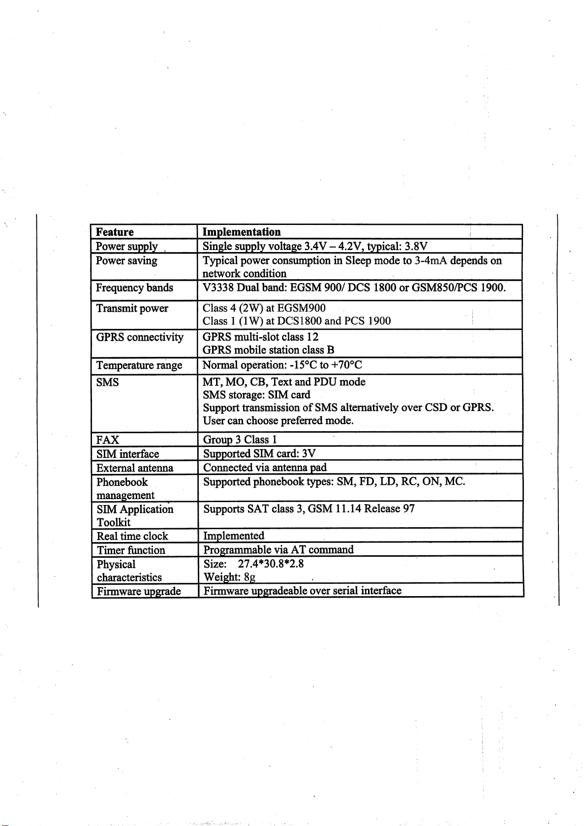
2.1. V3338 features at a glance ............................................................................................... ..... 6
3. Hardware Interface ............................................................................................................................. 7
3.1. Module Interface .................................................................................................................... 7
3.2. Pin description ........................................................................................................................ 7
3.3. Operating modes .................................................................................................................... 9
3.4. Power supply ........................................................................................................................ 10
3.5. Power up and power down scenarios ................................................................................... 11
3.5.1. Turn on V3338 ........................................................................................................ 1 1
3.5.2. Turn off V3338 ....................................................................................................... 1 2
3.5.3. Hardware Shut Off V33
3.5.4. Power saving ............................................................................................................ 12
3.6. Serial interfaces .................................................................................................................... 12
3.7. Audio interfaces ................................................................................................................... 13
3.8. DAI PCM Interface .............................................................................................................. 14
3.9. PWM and Alerter (needs software support) ......................................................................... 15
3.10. Antenna ................................................................................................................................ 15
3.11. SIM card interface ................................................................................................................ 16
3.12. Keypad Interface .................................................................................................................. 18
3.13. LCD Interface (Parallel display can not work onV3338) ............................................... 19
3.14. RTC backup .......................................................................................................................... 21
3.15. IOs ........................................................................................................................................ 21
3.16. External Interrupt ................................................................................................................. 21
3.17. Open-Drain Output Swith .................................................................................................... 22
3.18. ADC ..................................................................................................................................... 22
3.19. Digital Pin Electrical Characteristics ................................................................................... 23
3.20. Modem Hardware flow control PIN Description ................................................................. 26
3.21. Module sleep mode control .................................................................................................. 26
3.22. Behaviors of the RING indication line ................................................................................. 26
3.23. Network status indication LED lamp ................................................................................... 27
3.24. Network Signal Level Indication Pins .................................................................................. 27
4. Software application ......................................................................................................................... 28
4.1. Master mode (such as application for fixed wireless phone) ............................................... 28
4.2. Slave mode (standard GSM/GPRS module application) ...................................................... 28
4.2.1. AT command ............................................................................................................ 28
4.2.2. The hyper terminal configure method ...................................................................... 28
4.2.3. TCP/IP protocol ........................................................................................................ 29
5. Mechanics ........................................................................................................................................ 30
6. Interface board Reference EVB ....................................................................................................... 31
6.1 Standard GSM/GPRS module ................................................................................................. 31
6.2 Module apply for fixed wireless phone ................................................................................ 35
38 ...................................................................................... 12
3
Page 4
0 Version History
Data Version Description of change Author
2008-03-03 01.00 Origin George
2008-03-20 01.01 Changchun Zhu
2008-05-29 01.02
2008-09-11 01.03
2008-12-18 01.04
2009-02-15 01.05
2009-05-22 01.06
2010-09-30 01.07
Modem Hardware flow control PIN
Description
Add Behaviors of the RING line.
Add Behaviors of the Network LED.
Add Network signal level LED indication.
Modify Behaviors of the RI and Network
signal level line
Modify Pin of network led and signal level pin
Modify Pin of network led and signal level pin
on page 31 of the Reference SCH of Module
Exchange Pin41 from ADC0 to
on
V3338
-XX-XXXX-XXXX-
AU_MOUTL
A10
Xiao Youzhi
Xiao Youzhi
Xiao Youzhi
Xiao Youzhi
Changchun Zhu
Changchun Zhu
4
Page 5

1 Introduction
This document describes the hardware interface of the V3338 GS M/GPRS module which
can be integrated with a wide range of applications. This document can help you quickly
understandV3338 interface sp ecifications, electrical and mechanical details. With the help
of this document and otherV3338 applica tion notes, user guide, you can use V3338
module to design and set-up mobile applications quickly.
1.1. Related documents
[1] GSM 07.07:
[2] GSM 07.05: Digital cellular telecommunications (Phase 2+); Use of
[3] GSM 11.14: Digital cellular telecommunications system (Phase 2+);
[4] GSM 11.11: Digital cellular telecommunications system (Phase 2+);
[5] GSM 03.38: Digital cellular telecommunications system (Phase 2+);
[6] GSM 11.10
[7] GSM 07.10 Digital Cellular telecommunications system (Phase
[8] GSM 07.10 V7.1.0 Digital cellular telecommunications system (Phase
[9] GSM 07.07 V7.5.0
[12] UFT 09102006 UFT Wirless Phone feature
Digital cellular telecommunications (Phase 2+); AT
command set for GSM Mobile Equipment (ME)
Data Terminal Equipment – Data Circuit terminating
Equipment (DTE –DCE) interface for Short Message
Service (SMS) and Cell Broadcast Service (CBS)
Specification of the SIM Application Toolkit for the
Subscriber Identity Module –Mobile Equipment (SIM –
ME) interface
Specification of the Subscriber Identity Module –
Mobile Equipment (SIM – ME) interface
Alphabets and language-specific information
Digital cellular telecommunications system (Phase 2);
Mobile Station (MS) conformance specification; Part
1: Conformance specification
2+); Terminal Equipment to Mobile Station multiplexer
protocol, verion 7.2.0 Release 1998
2+);Terminal Equipment to Mobile Station
(TE-MS)multiplexer protocol
AT command set for GSM Mobile Equipment
5
Page 6
6
Page 7
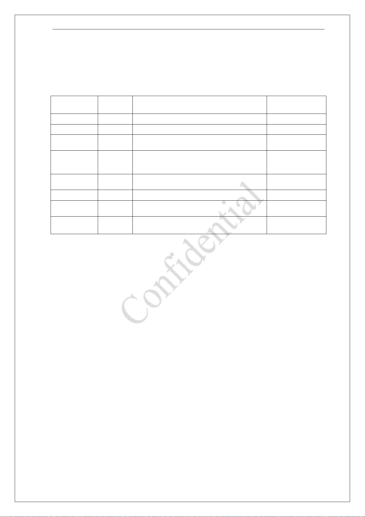
3. Hardware Interface
3.1. Module Interface
The 80 pins described in detail in following chapters:
Power supply
Serial interface
Analog audio interfaces
PCM interface
PWM
Antenna
SIM interface
Keyboard interface
LCD interface
Charger
RTC backup battery
IOs
External Interrupt
Open-Drain Output Switch
ADC
3.2. Pin description
Table 1: Pin description
V3338 module pin assignment :
No. Name I/O Description
1 PCM_IN I DAI PCM data input
2 PCM_CLK O DAI PCM clock output
3 PCM_SYNC I DAI frame synchronization input
4 PCM_RST I DAI reset signal input
5 PCM_OUT O DAI PCM data output
6 LCD_RSTB O Parallel display interface Reset Signal
7 IO14 I/O General purpose Input/Output pin, No.14/Can’t use in V3338
8 LCD_CS0 O Parallel display interface chip select 0 output
9 WATCHDOG O Watchdo g reset output, active low
10 EINT0 I External interrupt 0
11 EINT2 I External interrupt 2
12 COL0 I Keypad column 0
13 COL1 I Keypad column 1
14 COL2 I Keypad column 2
15 COL3 I Keypad column 3
16 COL4 I Keypad column 4
17 ROW0 O Keypad row 0
18 ROW1 O Keypad row 1
19 ROW2 O Keypad row 2
20 ROW3 O Keypad row 3
7
Page 8
21 ROW4 O Keypad row 4
22 IO31 I/O General purpose Inp ut/Output pin, No.31
23 EINT3 I External interrupt 3
24 CTS I UART1-Clear To Send
25 RTS O UART1-Request To Send
26 EINT1 I External interrupt 1
min typ max
27 VBACKUP power BAT_Backup Voltage Input
28 TXD3 O UART3-Transmit Data
29 TXD2 O UART2-Transmit Data
30 TXD1 O UART1-Transmit Data
31 RXD3 I UART3-Receive Data
32 RXD2 I UART2-Receive Data
33 RXD1 I UART-Receive Data
34 VDD O 2.8V
35 VBAT power System Power Voltage Input
36 GND Ground
37 VRSIM O Rugulator SIM Output
38 SIM_RST O SIM Reset
39 SIM_IO I/O SIM Input/Output
40 SIM_CLK O SIM Clock
Auxiliary ADC input 0 (Exchanged with AU_MOUTL on
41 ADC0* I
42 Suspend Do not link to anything or link to GND
43 LEDA O LED Driver, Paging Indicator
44 PWRKEY I Power on the module
45 GND Ground
46 EARN O Earphone amplifier negative output(-)
47 EARP O Earphone amplifier positive output(+)
48 MICIN I Microphone amplifier negative input(-)
49 MICIP I Microphone amplifier positive input(+)
50 AU_MOUTR O Audio analog output right channel
51 AUXI I Auxiliary hands free amplifier positive input(+)
52 GND Ground
53 VBAT
54 VBAT 3.3V 4.2V 4.6V
ADC1/Battery
55
ID I ADC
56 IO22 IO General purpose Input/Output pin, No. 22
57 System reset I System will reset when input active low (more than 1s low voltage)
58 IO21 I/O General purpose Input/Output pin, No. 21
59 LCD7 O Parallel display interface Data7
60 LCD6 O Parallel display interface Data6
61 LCD5 O Parallel display interface Data5/ Can’t use in V3338
62 LCD4 O Parallel display interface Data4/
63 LCD_WR O Parallel display interface Write Signal/
64 IO20 I/O General purpose Input/Output pin, No. 20
65 IO25/PWM I/O General purpose Input/Output pin, No.25
66 GND Ground
67 ANT Antenna
68 GND Ground
69 LCD_RD O Parallel display interface Read Signal/
70 LCD_A0 O Parallel display interface address output/
power Power input for RF
V3338
8
XX-XXXX
-
Can’t use in V3338
Can’t use in V3338
Can’t use in V3338
Can’t use in V3338
1.3V 1.8V 2.0V
min typ max
3.3V 4.2V 4.6V
XXXX
-
A10
-
min typ max
)
Page 9
71 IO30 I/O General purpose Input/Output pin 30
72 LCD0 O Parallel display interface Data0/
73 LCD1 O Parallel display interface Data1/
74 LCD2 O Parallel display interface Data2/
75 IO24 I/O General purpose Input/Output pin, No. 24
76 IO0 I/O General purpose Input/Output pin, No. 0
77 JTDI I JTAG-Data Input
78 JTMS I JTAG-Test Mode Select
79 JTRST I JTAG test port reset input
80 LCD3 O Parallel display interface Data3/
Can’t use in V3338
Can’t use in V3338
Can’t use in V3338
Can’t use in V3338
3.3. Operating modes
The following table summarizes the various operating modes, each operating modes is
referred to in the following chapters.
Table 2:Overview of operating modes
Mode Function
Normal
operation
GSM/GPRS
Sleep
Module will automatically go into Sleep mode if there is
no air link activation and no hardware interrupt (such as
GPIO interrupt or data on serial port).
In this case, the current consumption of module will
reduce to the minim.
During sleep mode, the module can still receive paging
message.
GSM IDLE Module has registered to the GSM network, and the
module is ready to send and receive.
GSM TALK CSD connection is going on between two subscribers. In
this case, the power consumption depends on network
condition and settings such as DTX off/on, FR/EFR/HR,
hopping sequences.
GPRS IDLE Module is ready for GPRS data transfer, but no data is
currently sent or received. In this case, power
consumption depends on network settings and GPRS
configuration (e.g. multi-slot settings).
GPRS
DATA
There is GPRS data in transfer (PPP or TCP or UDP). In
this case, power consumption is related with network
settings (e.g. power control level), uplink / downlink
data rates and GPRS configuration (e.g. used multi-slot
settings).
POWER
DOWN
The power management ASIC disconnects the power supply from the
base band part of the module, only the power supply for the RTC is
remained. Software is not active. The serial interfaces are not accessible.
Alarm
mode
RTC alert function launches this restricted operation while the module is
in POWER DOWN mode. V3338 will not be registered to GSM
network and only parts of AT commands can be available.
9
Page 10
3.4. Power supply
The power supply must be able to provide sufficient current up to 2A.
For the VBAT input, a local bypass capacitor is recommended. A capacitor (above 100µF,
low ESR) is recommended. Multi-layer ceramic chip (MLCC) capacitors can provide the
best combination of low ESR and small size but may not be cost effective. A lower cost
choice may be a 100 µF tantalum capacitor (low ESR) with a small (1 µF to 10µF) ceramic
in parallel, which is illustrated as following figure. And the capacitors should put as closer
as possible to the V3338 VBAT (RF) pins. A voltage regulator diode should been add
between the Vbat and Gnd, and the BZV55C5V1 of Philips could been used. The following
figure is the recommended circuit.
Figure 1:VBAT input
10
Page 11
Table3: Power supply pins on the half-circle connector
Num Name Function I/O Min
(V)
35, 53, 54 VBAT
36, 45, 52,
66, 68
Minimizing power losses
Please pay special attention to the supply power when you are designing your applications.
Please make sure that the input voltage will never drops below 3.3V even in a transmit
burst during which the current consumption may rise up to 2A. If the power voltage drops
below 3.3V, the module may be switched off. You should also take the resistance of the
power supply lines on the host board or of battery pack into account.
GND GND GND
Power
Supply
Input 3.3 4.2 4.6
Type
(V)
Max
(V)
Note
Please make sure
that the input
voltage will never
drops below 3.3V
even in a transmit
burst during which
the current
consumption may
rise up to 2A.
3.5. Power up and power down scenarios
3.5.1. Turn on V3338
MD231 can be turned on by following two ways:
z Via PWRKEY pin: You can turn on the V3338 to normal operating mode by driving
the PWRKEY to a low level voltage for 1500ms;
z Via RTC interrupt: starts ALARM modes;
z For some application system, we can connect the “PWRKEY” to “GND” so that the
module will be turn on as soon as the 3.8V power supply to the module. But, if
“PWRKEY” linked to “GND”, other keypad pin could not work. Here is a circuit to
make the module power on automatically. GPIO26 is the pin78 of the V3338. If the
module power on, the GPIO26 will output high level, on consequence, the
“PWR_KEY” will be high level so that other keypad pin could work.
11
Page 12
3.5.2. Turn off V3338
V3338 can be truned off by following two ways:
Driving the PWRKEY to a low level for 1500ms when module working
z
z
Use “AT + CKPD=”P”, 50” command to turn off V3338 module.
3.5.3. System reset for V3338
You can reset V3338 by driving the “system reset” pin to a low level voltage for 500ms. If
V3338 blocked in hardware or software, you can not turn off V3338 by “PWRKEY” pin
or by AT command, the only way is driving the “System reset” pin to low level for more
than 1s and then high level. The module will reset.
3.5.4. Power saving
3.6. Serial interfaces
V3338 provides
UARTs provide full duplex serial communication channels between the module and
external devices.
Serial Port can be used for CSD FAX, GPRS service and send AT command of controlling
module. Serial port supports the communication rate as following:
1200, 2400, 4800, 9600 (Default), 19200, 38400, 57600, 115200
The serial port
The follow table is the pin definition of UART.
3 UARTs with hardware flow control and speed up to 921600 bps. The
Table4: UART interface of the MD231
Pin Name Function Pin Name Function
12
Page 13

30 TXD1
29 TXD2
28 TXD3
24 CTS UART1-Clear To
UART1-Transmit
Data
UART2-Transmit
Data
UART3-Transmit
Data
Send
33 RXD1
32 RXD2
31
25
RXD3
RTS UART1-Request
UART-Receive
Data
UART2-Receive
Data
UART3-Receive
Data
To Send
The reference design of standard serial port level witching circuit is as follow figure:
Figure2 The reference diagram of standard serial port level switching circuit
3.7. Audio interfaces
The module provides two audio channels:
EAR and MIC, used for microphone and receiver;
AUXI and AU_MOUT, used for line in and line out;
The audio should be far away from the radio part to reduce TD noise from radio.
The audio pins definitions are as follow table:
Table5: Audio interface of the V3338
Pin Name Function Pin Name Function
Audio analog
50 AU_MOUTR
output right
channel
51 AUXI
13
Auxiliary hands
free amplifier
positive input(+)
Page 14

46 EARN
48 MICIN
Earphone negative
output(-)
Microphone
amplifier negative
input(-) output
47 EARP
49
MICIP
Earphone positive
output(+)
Microphone
amplifier positive
input(+) output
It is suggested that you adopt following matching circuit in order to satisfy speaker effect.
The difference audio signals have to be layout according to difference signal layout rules. If
you want to adopt an amplifier circuit for audio, we commend National company’s
LM4890. But you can select it according to your needs.
The audio reference design as follow chart:
Figure3 The reference design of audio
The microphone bias electric circuit was designed in V3338. The MIC_BIAS DC
characteristics see the table 6.
Table 6:MIC_BIAS DC Characteristics
Parameter Minimum Typical Maximum Units
Microphone Bias
1.9 V
Voltage (MIC_BIAS)
Source Current 2 mA
All voice band data paths comply with the GSM 03.50 specification. Mono hands-free
audio are also provided. The audio stereo path facilitates CD-quality playback and voice
playback through a headset.
3.8. DAI PCM Interface
The Digital Audio Interface (DAI) block communicates with the System Simulator for
FTA or external Bluetooth modules. To communicate with the external Bluetooth module,
the master-mode PCM interface and master-mode I2S/EIAJ interface are supported. The
clock of PCM interface is 256 kHz, and the frame sync is 8 kHz. Both long sync and short
sync interfaces are supported. The PCM interface can transmit 16-bit stereo or 32-bit mono
8 kHz sampling rate voice signal. Table 6 show the pin map of DAI PCM.
I2S/EIAJ interface is designed to transmit high quality audio data. I2S/EIAJ can support 32
kHz, 44.1kHz, and 48kHz sampling rate audio signals. The clock frequency of I2S/EIAJ
can be 32×(sampling frequency), or 64×(sampling frequency). For example, to transmit a
14
Page 15

44.1 kHz CD-quality music, the clock frequency should be 32 × 44.1 kHz = 1.4112 MHz or
64×44.1 kHz = 2.8224 MHz.
Table 7:
Pin Name Function Pin Name Function
4 PCM_RST DAI reset signal input 3 PCM_SYNC
2 PCM_CLK DAI PCM clock output 1 PCM_IN DAI PCM data input
5 PCM_OUT DAI PCM data output
Pin mapping of DAI, PCM interfaces
General purpose
Input/Output pin 24
3.9. PWM and Alerter (needs software support)
The output of the PWM signal should supported by software. We can do custom software
for users to support PWM signal.
Table8: Alerter and PWM interface of the V3338
Pin Name Function Pin Name Function
Pulse-width
modulated signal
for buzzer
65 IO25/PWM
Pulse-width
modulated signal
75 IO24/Alerter
3.10. Antenna
The RF interface has an impedance of 50Ω. The antenna cable can be soldered to the pad.
Pay attention, the line between the V3338 ante nna pin and antenna connection should be
thick and short. It is better to use filter circuit to fit 50 ohms.
Table9: RF output power:
Frequency Max Min
GSM850 33dBm±2dB 5dBm±5dB
E-GSM900 33dBm±2dB 5dBm±5dB
DCS1800 30dBm±2dB 0dBm±5dB
PCS1900 30dBm±2dB 0dBm±5dB
Table10: Module RF receive sensitivity:
Frequency Receive
sensitivity
GSM850 <-106dBm
E-GSM900 <-106dBm
DCS1800 <-104dBm
PCS1900 <-104dBm
Table11: V3338 receive/transmit frequency
Frequency Receive Transmit
GSM850 869~894MHz 824-849MHz
E-GSM900 925~960MHz 800-915MHz
15
Page 16

DCS1800 1710~1785 MHz
1805~1800
MHz
1930~1990
PCS1900 1850~1910 MHz
MHz
According to the application, should use GSM900/DCS1800 Dual-band antenna or
GSM850/PCS1900 Dual-band antenna.
3.11. SIM card interface
The V3338 contains a dedicated smart card in terface to allow the MCU access to the SIM
card.
The SIM interface supports the functionality of the GSM Phase 1 specification and also supports
the functionality of the new GSM Phase 2+ specification for FAST 64 kbps SIM (intended for use with a
SIM application Tool-kit).
The SIM card interface circuitry of PMU meets all ETSI and IMT-2000 SIM interface
requirements. It provides level shifting needs for low voltage GSM controller to
communicate with either 1.8V or 3V SIM cards. All SIM cards contain a clock input, a
reset input, and a bi-directional data input/output. The clock and reset inputs to SIM cards
are level shifted from the supply of digital IO (Vio) of baseband chipset to the SIM supply
(Vsim). The bi-directional data bus is internal pull high with 10kohm resistor.
All pins that connect to the SIM card (Vsim, SRST, SCLK, SIO) withstand over 5kV
of human body mode ESD. In order to ensure proper ESD protection, careful board
layout is required.
The interface of SIM is as follow table:
Tbale12: The SIM pins on the Module
Num Name Function
37 VRSIM 2.8V power supply for SIM card
38 SIM_RST SIM card RESET output
39 SIM_IO SIM card data output and input
40 SIM_CLK SIM card clock output
Table 13: SIM Interface Electrical Specifications
SIM Voltage
Output voltage (V_SIM) Register
VSIM_SEL=L
Register
VSIM_SEL=H
Output current (Isim_max)
Line regulation
Load regulation
1.71 1.8 1.89 V
2.82 3.0 3.18 V
20
mA
4 mV
15 mV
Parameter Conditions Min. T
Interface to 3 V SIM Card
Volrst I = 20 μA
16
ypical Max. Unit
0.4 V
Page 17

Vohrst I = -200 μA
0.9*VSI
M
V
Volclk I = 20 μA
Vohclk I = -200 μA
Vil
0.9*VSI
M
Vihsio , Vohsio I = ±20 μA VSIM-0.4
Iil Vil = 0 V
Vol Iol = 1 mA, SIMIO ≤ 0.23 V
Interface to 1.8 V SIM Card
Volrst I = 20 μA
Vohrst I = -200 μA
0.9*VSI
M
Volclk I = 20 μA
Vohclk I = -200 μA
0.9*VSI
M
0.4 V
0.4 V
-1 mA
0.4 V
0.2*VSI
M
0.2*VSI
M
V
V
V
V
V
V
Vil
Vihsio , Vohsio I = ±20 μA VSIM-0.4
Iil Vil = 0 V
Vol Iol = 1 mA, SIMIO ≤ 0.23 V
SIM Card Interface Timing
SIO pull-up
resistance to VSIM
SRST, SIO rise/fall
times
SCLK rise/fall times
VSIM = 3, 1.8 V, load with
30 pF
VSIM = 3 V, CLK load with
8 10 12 kΩ
30 pF
VSIM = 1.8 V, CLK load
with 30 pF
SCLK frequency CLK load with 30 pF 5
SCLK duty cycle
SIMCLK Duty = 50%,
fsimclk = 5 MHz
47
0.4 V
V
-1 mA
0.4 V
1 μs
18 ns
50 ns
MHz
53 %
SCLK propagation
delay
30 50 ns
Following is a reference circuit about SIM interface. We recommend a Electrostatic
discharge device ST (www.st.com) ESDA6V1W5 or ONSEMI (www.onsemi.com)
SMF05C for “ESD ANTI”.
17
Page 18

Figure4 The reference design of SIM Socket
3.12. Keypad Interface
The keypad can be divided into two parts: one is the keypad interface including 6 columns
and 5 rows with one dedicated power-key, as shown in Fig. 5. the other is the key detection
block which provides key pressed, key released and de-bounce mechanisms. Each time the
key is pressed or released, i.e. something different in the 5 x 6 matrix or power-key, the key
detection block senses the change and recognizes if a key has been pressed or released.
This keypad can detect one or two key-pressed simultaneously with any combination. Since
the key press detection depends on the HIGH or LOW level of the external keypad
interface, if keys are pressed at the same time and there exists a key that is on the same
column and the same row with the other keys, the pressed key cannot be correctly decoded.
For example, if there are three key presses: key1 = (x1, y1), key2 = (x2, y2), and key3 =
(x1, y2), then both key3 and key4 = (x2, y1) are detected, and therefore they cannot be
distinguished correctly. Hence, the keypad can detect only one or two keys pressed
simultaneously at any combination. More than two keys pressed simultaneously in a
specific pattern retrieve the wrong information.
18
Page 19

Figure5 The Typical Keypad Interface Circuit
3.13. LCD Interface (Parallel display can not work on
V3338)
V3338 contains a versatile LCD controller whic h is optimized for multimedia applications.
This controller supports many types of LCD modules and contains a rich feature set to
enhance the functionality. These features are:
z Up to 320 x 240 resolution
z Supports 8-bpp (RGB332), 12-bpp (RGB444), 16-bpp (RGB565), 18-bit (RGB666)
and 24-bit (RGB808) color depths
z Layers Overlay with individual vertical and horizontal size, vertical and horizontal
offset, source key, opacity and display rotation control(90°,180°, 270°, mirror and
mirror then 90°, 180° and 270°)
z Color Look-Up Table
For parallel LCD modules, this special LCD controller can reuse external memory interface
or use dedicated 8/9-bit parallel interface to access them and 8080 type interface is
supported. It can transfer the display data from the internal SRAM or external SRAM/Flash
Memory to the off-chip LCD modules.V3338 will not support parallel LCD.
For serial LCD modules, this interface performs parallel to serial conversion and both 8and 9- bit serial interface is supported. The 8-bit serial interface uses four pins – LSCE#,
LSDA, LSCK and LSA0 – to enter commands and data.
Meanwhile, the 9-bit serial interface uses three pins – LSCE#, LSDA and LSCK – for the
same purpose. Data read is not available with the serial interface and data entered must be 8
bits.
Figure 6 shows the timing diagram of this serial interface. When the block is idle, LSCK is
forced LOW and LSCE# is forced HIGH. Once the data register contains data and the
interface is enabled, LSCE# is pulled LOW and remain LOW for the duration of the
transmission.
19
Page 20

Figure 6 LCD Interface Transfer Timing Diagram
Tbale14: The LCD pins on the Module
Num Name Function
8 LCD_CS0 Parallel display interface chip select 0 output
70 LCD_A0 Parallel display interface address output
6 LCD_RSTB Parallel display interface Reset Signal
63 LCD_WR Parallel display interface Write Signal
59 LCD_D7 Parallel display interface Data7
60 LCD_D6 Parallel display interface Data6
61 LCD_D5 Parallel display interface Data5
62 LCD_D4 Parallel display interface Data4
80 LCD_D3 Parallel display interface Data3
74 LCD_D2 Parallel display interface Data2
73 LCD_D1 Parallel display interface Data1
72 LCD_D0 Parallel display interface Data0
76 IO0/LCD8 Parallel display interface Data8
69 LCD_RD Parallel display interface Read Signal
7 LCD_CS1/IO14 Parallel display interface chip select 1 output
In addition, V3338 provide another feature, that is, LCD controller can be used for
memory card. Only MC_CLK and LCD_D[4:0] is used for MSDC interface. LCD
controller generates MC_CLK when writing or reading offset 6000h.
The timing of memory card data and clock is shared with LCD_PCNF0. MC_CLK is
shared with BPI_BUS2 and BPI_BUS3,and the MC_CLK output is enabled by
ACIF_CON0[15:14]. To control memory cards, extra ACIF_CON0 settings are required.
LCD_D0~LCD_D4 has nature of pull-down when in input mode, which may violate
MSDC access nature (ex. Most SD card expect data to be high when in idle). Besides the
MC_CLK output enable setting, in order to accommodate MSDC nature, PD (pull-down)
of LCD_D0 to LCD_D4 should be disabled by use of ACIF_CON0[12]. As for more detail
of ACIF_CON0 setting, please refer to GPIO functional specification.
20
Page 21

3.14. RTC backup
The Real Time Clock (RTC) module provides time and data information. The clock is
based on a 32.768KHz oscillator with an independent power supply. When the module is
powered off, a dedicated regulator supplies the RTC block. If the main battery is not
present, a backup supply such as a small mercury cell battery or a large capacitor is used
through the pin27 of VBACKUP. Figure 7 give the example diagram of the two ways. In
addition to providing timing data, an alarm interrupt is generated and can be used to power
up the baseband core via the BBWAKEUP pin. Regulator interrupts corresponding to
seconds, minutes, hours and days can be generated whenever the time counter value
reaches a maximum value (e.g., 59 for seconds and minutes, 23 for hours, etc.). The year
span is supported up to 2127. The maximum day-of-month values, which depend on the
leap year condition, are stored in the RTC block.
Figure7 The RTC battery diagram for the module
3.15. IOs
V3338 module has several IO pins which are configurable according to customer’s
requirement. We can do custom software for users.
Upon hardware reset (SYSRST#), IOs are all configured as inputs.
3.16. External Interrupt
V3338 module has several IO pins which are configurable according to customer’s
requirement. We can do custom software for users.
The four external interrupts can be used for different kind of applications, mainly for event
detections: detection of hand free connection, detection of hood opening, detection of
21
Page 22

battery charger connection.
Since the external event may be unstable in a certain period, a de-bounce mechanism is
introduced to ensure the functionality. The circuitry is mainly used to verify that the input
signal remains stable for a programmable number of periods of the clock. When this
condition is satisfied, for the appearance or the disappearance of the input, the output of the
de-bounce logic changes to the desired state. Note that, because it uses the 32 KHz slow
clock for performing the de-bounce process, the parameter of de-bounce period and
de-bounce enable takes effect no sooner than one 32 KHz clock cycle (~31.25us) after the
software program sets them. However, the polarities of EINTs are clocked with the system
clock. Any changes to them take effect immediately.
The ENT pins can be configurable to “EDGE/LEVEL” according to the external signal.
3.17. Open-Drain Output Swith
The LEDA pin and VIB pin are Open-Drain Output Switch.
Two built-in open-drain output switches drive the vibrator motor and Keypad LED in the
module. Each switch is controlled by baseband with enable registers. The switch of keypad
LED can sink 150mA. Figure 8 give one example of the LEDA application.
Table 18 VIB and LEDA Pins On The Module
Num Name Function
43 LEDA LED Driver
Figure8 The reference application of LEDA
3.18. ADC
V3338 provides one auxiliary ADC (General purpose analog to digital converter.) as
voltage input pin, which can be used to detect the values of some external items such as
22
Page 23

voltage 、 temperature etc. For module application, user can use AT command
“AT+CADC#” to read the voltage value added on ADC pin.
The functional specifications of the auxiliary ADC are listed in the following table.
Table 19 The Functional specification of Auxiliary ADC
Symbol Parameter Min Typical Max Unit
N Resolution
10
Bit
FC Clock Rate 0.1 1.0833 5 MHz
FS Sampling Rate @ N-Bit
Input Swing 1.0
T Operating Temperature -20
Current Consumption Power-up
Power-Down
300
1
5/(N+1) MSPS
AVDD V
80 ℃
μA
μA
3.19. Digital Pin Electrical Characteristics
About the digital pin electrical characteristics of V3338, please reference the table 20.
Table 20: Module digital electrical characteristics
Based on I/O power supply (VDD33) = 3.3 V
Vil (max) = 0.8 V
Vih (min) = 2.0 V
Pin Name Driving(mA) Pull Vol at
max.
Iol
Voh at
max.
Ioh
Cin(pF)
PU/PD
Resistor(K ohm)
(min, typical,
max)
IO20
IO21
IO22
PCM_CLK
PCM_OUT
PCM_IN
PCM_RST
PCM_SYNC
IO24/ALERTER
IO25/PWM
JRTCK
JTRST
JTCK
JTDI
JTMS
2 PD 0.4 2.4
2 PD 0.4 2.4 40, 75, 190 5.2
2 PU 0.4 2.4
6 PU 0.4 2.4 40, 75, 190 5.2
6 PD 0.4 2.4 40, 75, 190 5.2
6 PU 0.4 2.4 40, 75, 190 5.2
6 PU 0.4 2.4 40, 75, 190 5.2
6 PU 0.4 2.4 40, 75, 190 5.2
4 PD 0.4 2.4 40, 75, 190 5.2
4 PD 0.4 2.4 40, 75, 190 5.2
6 PU 0.4 2.4 40, 75, 190 5.2
2 PD 0.4 2.4 40, 75, 190 5.2
input only PU
40, 75, 190 5.2
PU 0.4 2.4 40, 75, 190 5.2
PU 0.4 2.4 40, 75, 190 5.2
23
5.2
5.2
Page 24

JTDO
IO0/LCD_D8
LCD_D7
LCD_D6
LCD_D5
LCD_D4
LCD_D3
LCD_D2
LCD_D1
LCD_RSTB
LCD_WR
LCD_RD
LCD_D0
LCD_A0
LCD_CS0
IO14/LCD_CS1
WATCHDOG
IO30/EA0
SRCLKENAI
COL4
COL3
COL2
COL1
COL0
ROW4
ROW3
ROW2
ROW1
ROW0
EINT0
EINT1
EINT2
EINT3
UTXD1
UCTS1
URTS1
UTXD3
URXD3
URXD2
URXD1
UTXD2
PU 0.4 2.4 40, 75, 190 5.2
PD 0.4 2.4 40, 75, 190 5.2
PD 0.4 2.4 40, 75, 190 5.2
PD 0.4 2.4 40, 75, 190 5.2
PD 0.4 2.4 40, 75, 190 5.2
PD 0.4 2.4 40, 75, 190 5.2
PD 0.4 2.4 40, 75, 190 5.2
PD 0.4 2.4 40, 75, 190 5.2
PD 0.4 2.4 40, 75, 190 5.2
PU 0.4 2.4 40, 75, 190 5.2
PU 0.4 2.4 40, 75, 190 5.2
PU 0.4 2.4 40, 75, 190 5.2
PD 0.4 2.4 40, 75, 190 5.2
PU 0.4 2.4 40, 75, 190 5.2
PU 0.4 2.4 40, 75, 190 5.2
PU 0.4 2.4 40, 75, 190 5.2
0.4 2.4
5.2
PD 0.4 2.4 40, 75, 190
PD 0.4 2.4 40, 75, 190 5.2
PU 0.4 2.4 40, 75, 190 5.2
PU 0.4 2.4 40, 75, 190 5.2
PU 0.4 2.4 40, 75, 190 5.2
PU 0.4 2.4 40, 75, 190 5.2
PU 0.4 2.4 40, 75, 190 5.2
PU
PU
0.4 2.4
0.4 2.4
0.4 2.4
0.4 2.4
0.4 2.4
5.2
5.2
5.2
5.2
5.2
40, 75, 190 5.2
40, 75, 190 5.2
PU 0.4 2.4 40, 75, 190 5.2
PU 0.4 2.4 40, 75, 190 5.2
PU 0.4 2.4 40, 75, 190 5.2
PU 0.4 2.4 40, 75, 190 5.2
PU 0.4 2.4 40, 75, 190 5.2
PU 0.4 2.4 40, 75, 190 5.2
PU 0.4 2.4 40, 75, 190 5.2
PU 0.4 2.4 40, 75, 190 5.2
PU 0.4 2.4 40, 75, 190 5.2
PU 0.4 2.4 40, 75, 190 5.2
About the digital IO LDO (VIO) is a regulator that could source 100mA (max) with 2.8V
output voltage. It supplies the baseband circuitry of the Module. The LDO is optimized for
very low quiescent current and will power up at the same time as the digital core LDO.
Table21 show the electrical characteristics of VIO.
24
Page 25

Table 21 VIO electrical characteristics
VBAT = 3 V ~ 5 V, minimum loads applied on all outputs, unless other noted. Typical values are
at TA = 25 °C.
Parameter Conditions Min. Typical Max. Unit
Digital IO Voltage
Output voltage (V_IO)
2.7 2.8 2.9 V
Output current (Iio_max)
Line regulation
Load regulation
60
mA
5 mV
30 mV
25
Page 26

3.20. Modem Hardware flow control PIN Description
Flow control is essential to prevent loss of data or avoid errors when, in a data or fax call,
the sending device is transferring data faster than the receiving side is ready to accept.
When the receiving buffer reaches its capacity, the receiving device should be capable to
cause the sending device to pause until it catches up.
There are basically two approaches to regulate data flow: software flow control and
hardware flow control. Hardware flow control sets or resets the RTS/CTS wires. This
approach is faster and more reliable, and therefore, the better choice. When the High
Watermark is reached, CTS is set inactive until the transfer from the buffer has completed.
When the Low Watermark is passed, CTS goes active once again.
If the Module be used as modem with hardware flow control, PIN function will be as
follow description:
Table22: Hardware flow control PIN description:
No. Name PIN I/O Description
1 DCD 28 O Data Carrier Detected
2 TXD 30 O Transmitted Data
3 RXD 33 I Received Data
4 DSR 78 I Data Set Ready
5 GND GND GND Signal Ground
6 DTR 31 O Data Terminal Ready
7 CTS 24 I Clear To Send
8 RTS 25 O Request To Send
9 RI 11* O Ring Indicator
3.21. Module sleep mode control
Our Module support two ways to control module enter sleep mode or not:
1) Hardware control method: DSR(Pin78) is used for hardware sleep mode control.
LOW Level: disable module enter sleep mode;
HIGH Level: enable module enter sleep mode.
2) Software control method: AT command “AT+ESLP”
“AT+ESLP=0”: disable module enter sleep mode;
“AT+ESLP=1”: enable module enter sleep mode.
NOTE1: Module default software value is disable enter sleep mode.
NOTE2: If module enter sleep mode, the AT command can not be sent to module normally.
3.22. Behaviors of the RING indication line
V3338: Pin11 (GPIO42) is used for Ring indication when network event. The working state of this pin
is listed in following table:
Table 23: The Behaviors of the RING line
State RI respond
Standby High
26
Page 27

Change low, then:
Voice calling
1) Change to high when establish calling.
2) Sender hang up, change to high.
When receive SMS, The ring will change to
SMS
LOW and hold LOW level at least 200 ms,
then change to HIGH.
3.23. Network status indication LED lamp
V3338:Pin22(GPIO31 ) is used to drive a network status indication LED lamp. The working state of
this pin is listed in following table:
Table 23: Working state of network status indication LED pin
State Module function
Off Module is not running
64ms On/800ms Off Module does not find the network
64ms On/3000ms Off Module find the network
64ms On/300ms Off GPRS communication
3.24. Network Signal Level Indication Pins
V3338: Pin75 (GPIO24), Pin76 (GPIO0), Pin77 (GPIO27) are used to indication the network signal
level. The working state of this pin is listed in following table:
Table 24: Network signal level indication pins
State(Pin77,Pin76,Pin75) Network signal level
0,0,0 No signal
0,0,1 Signal Low
0,1,1 Signal Middle
1,1,1 Signal High
Note: State 0: Low Level;
State 1: High Level.
27
Page 28

4. Software application
The module can be used in master mode and slave mode.
4.1. Master mode (such as application for fixed wireless
phone)
In master mode, the module acted as main board of mobile terminal. The LCD or melody
processor can be connected to the module via data and address bus. Users can control the
module via keyboard and the MMI software can be customized according to requirement.
Please get schematic information from chap 6.2.
4.2. Slave mode (standard GSM/GPRS module
application)
In slave mode, the module communicated with master MCU via UART interface using AT
commands.
Please get schematic information from chap 6.1.
4.2.1. AT command
Please get detail information from refer[10]
4.2.2. The hyper terminal configure method
User can control the V3338 module using hyper terminal to send AT Command. The
configuration in hyper terminal:
Bits per second: 115200 (depends on SW)
Data bits: 8
28
Page 29

Parity: None
Stop bits: 1
Flow control: None
4.2.3. TCP/IP protocol
The module can support TCP/IP protocol. Please get detail information from reference
[11].
29
Page 30

5. Mechanics
30
Page 31

6. Interface board Reference EVB
6.1 Standard GSM/GPRS module
31
Page 32

32
Page 33

33
Page 34

34
Page 35

6.2 Module apply for fixed wireless phone
35
Page 36

36
Page 37

37
Page 38

38
Page 39

39
 Loading...