

Page 1
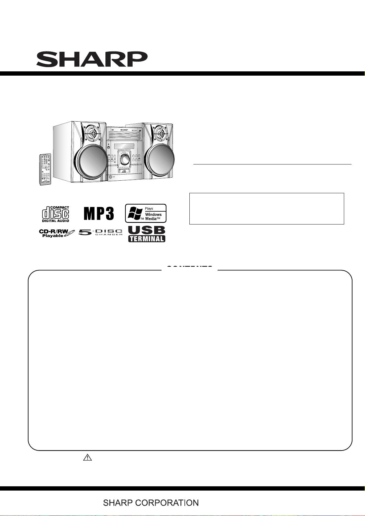
XL-UH260
SERVICE MANUAL
No. S2603XLUH260/
MICRO COMPONENT SYSTEM
CONTENTS
CONTENTS
PRECAUTIONS FOR USING LEAD-FREE SOLDER
CHAPTER 1. GENERAL DESCRIPTION
[1] IMPORTANT SERVICE NOTES ........... .......1-1
[2] SPECIFICATIONS........................................1-2
[3] NAMES OF PARTS......................................1-3
CHAPTER 2. ADJUSTMENTS
[1] CD Section....................................................2-1
[2] TEST MODE.................................................2-2
[3] Standard Specification of Stereo System
Error Message Display Contents..................2-4
[4] CD Changer Mechanism Section ................2-5
MODEL
XL-UH260 Micro Component System consisting of
XL-UH260 (main unit) and CP-UH260 (speaker system).
• In the interests of user-safety (Required by safety regulations in some countries) the set should be restored to its
original condition and only parts identical to those specified
be used.
CHAPTER 5. CIRCUIT DESCRIPTION
[1] WAVEFORMS OF SERVO CIRCUIT..............5-1
[2] VOLTAGE................................................ ......5-3
CHAPTER 6. CIRCUIT SCHEMATICS AND PARTS
LAYOUT
[1] NOTES ON SCHEMA TIC DIAGRAM.............6-1
[2] TYPES OF TRANSISTOR AND LED.............6-1
[3] WIRING SIDE OF PWB/SCHEMATIC
DIAGRAM.......................................................6-2
CHAPTER 7. FLOWCHART
[1] TROUBLESHOOTING....................................7-1
XL-UH260
CHAPTER 3. MECHANICAL DESCRIPTION
[1] REMOVING AND REINSTALLING THE MAIN
PARTS..........................................................3-1
[2] DISASSEMBLY.............................................3-3
CHAPTER 4. DIAGRAMS
[1] BLOCK DIAGRAM........................................4-1
Parts marked with " " are important for maintaining the safety of the set. Be sure to replace these parts with specified
ones for maintaining the safety and performance of the set.
– 1
CHAPTER 8. OTHERS
[1] FUNCTION TABLE OF IC ..............................8-1
[2] FL DISPLAY..................................................8-10
Parts Guide
This document has been published to be used for after
sales service only.
The contents are subject to change without notice.
Page 2
XL-UH260
PRECAUTIONS FOR USING LEAD-FREE SOLDER
1. Employing lead-free solder
"MAIN, POWER, SPEAKER, REFLASH MICOM, DISPLAY, USB, JACK, LED, SUB, CD MP3, SPEAKER LED
PWB, CD MOTOR (PWB ONLY), CD CHANGER (PWB ONLY)" of this model employs lead-free solder.
The LF symbol indicates lead-free solder, and is attached on the PWB and service manuals.The alphabetical
character following LF shows the type of lead-free solder.
Example:
Indicates lead-free solder of tin, silver and copper.
2. Using lead-free wire solder
When fixing the PWB soldered with the lead-free solder, apply lead-free wire solder. Repairing with
conventional lead wire solder may cause damage or accident due to cracks.use a dedicated soldering bit, if you
are not familiar with how to obtain lead-free wire solder or soldering bit, contact
branch in your area.
As the melting point of lead-free solder (Sn-Ag-Cu) is higher than the lead wire solder by
40 C, we recommend you to use a dedicated soldering bit, if you are nto familiar with how to obtain lead-free
wire solder or soldering bit, contact our service station or service branch in your area.
our service station or service
Soldering
3.
As the melting point of lead-free solder (Sn-Ag-Cu) is about 220 C which is higher than the conventional lead
solder by 40 C,and as it has poor solder wettability, you may be apt to keep the soldering bit in contact with the
PWB for extended period oftime. However, since the land may be peeled of for the maximum heat-resistance
temperature of parts may be exceeded,
remove the bit from the PWB as soon as you confirm the steady soldering condition. Lead-free solder contains
more tin, and the end of the soldering bit may be easily corrected. Make sure to turn on and off the power of the
bit as required. If a different type of solder stays on the tip of the soldering bit,it is alloyed with lead-free solder.
Clean the bit after every use of it. When the tip of the soldering bit is blackened during use, file it with steel wool
or fine sand paper. Be careful when replacing parts with polarity indication on the PWB silk.
Lead-free wire solder for servicing
Ref No.
PWB-A 92LPWB6480MANS
PWB-B 92LPWB6480DPLS
PWB-C
PWB-D
PWB-E
PWB-F
Parts No.
92LPWB6475CDUS
92LPWB6274LEDS
QPWBF0027AWZZ
QPWBF1055AWZZ
MAIN (A1), POWER (A2), SPEAKER (A3), REFLASH MICOM (A4)
DISPLAY (B1), USB (B2), JACK (B3), LED (B4), SUB (B5)
CD MP3
SPEAKER LED
CD MOTOR (PWB ONLY)
CD CHANGER (PWB ONLY)
Description
– 2
i
Page 3
XL-UH260
CHAPTER 1.
FOR A COMPLETE DESCRIPTION OF THE OPERATION OF
THIS UNIT, PLEASE REFER TO THE OPERATION MANUAL.
BEFORE RETURNING THE AUDIO PRODUCT
(Fire & Shock Hazard)
Before returning the audio product to the user, perform
the following safety checks.
1. Inspect all lead dress to make certain that leads are not
pinched or that hardware is not lodged between the
chassis and other metal parts in the audio product.
2. Inspect all protective devices such as insulating
materials, cabinet, terminal board, adjustment and
compartment covers or shields, mechanical insulators
etc.
3. To be sure that no shock hazard exists, check for
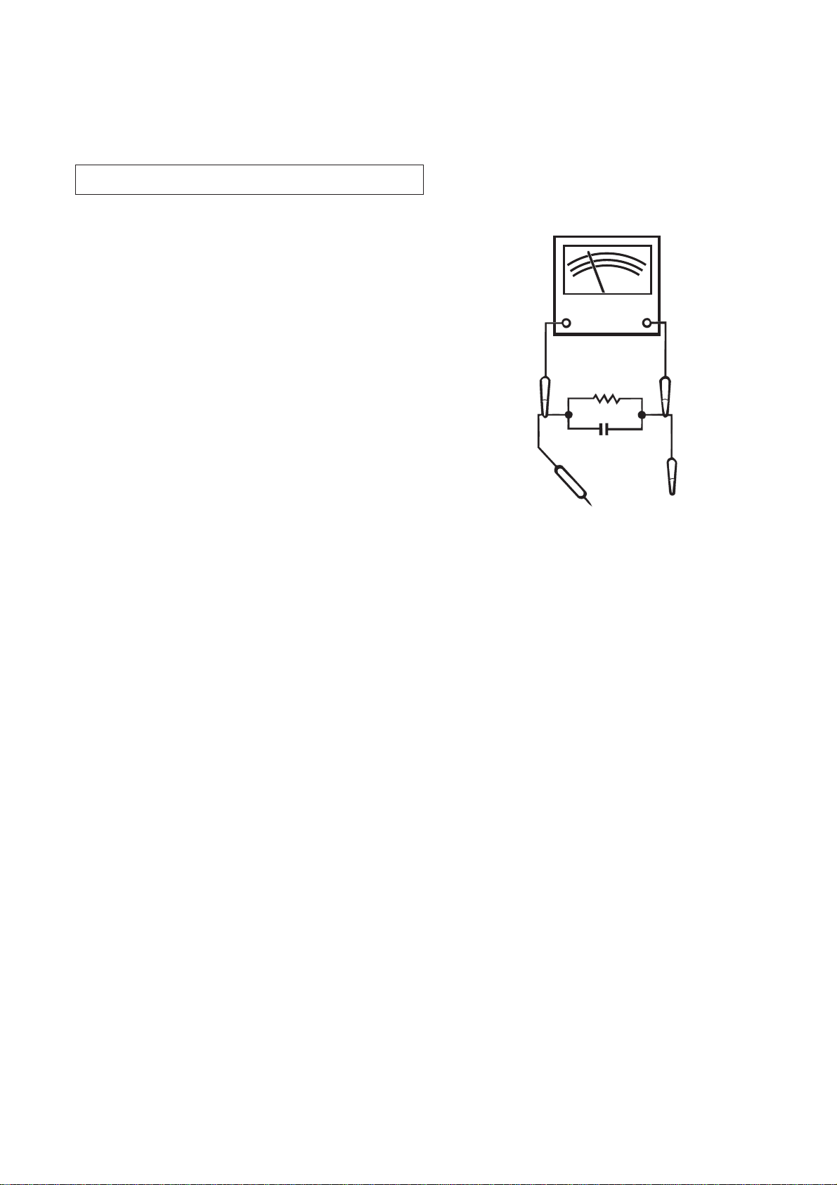
leakage current in the following manner.
Plug the AC line cord directly into a 120 volt AC outlet.
*
* Using two clip leads, connect a 1.5k ohm, 10 watt
resistor paralleled by a 0.15µF capacitor in series
with all exposed metal cabinet parts and a known
earth ground, such as conduit or electrical ground
connected to earth ground.
Use a VTVM or VOM with 1000 ohm per volt, or
*
higher, sensitivity to measure the AC voltage drop
across the resistor (See diagram).
* Connect the resistor connection to all exposed metal
parts having a return path to the chassis (antenna,
metal cabinet, screw heads, knobs and control shafts,
escutcheon, etc.) and measure the AC voltage drop
across the resistor.
GENERAL DESCRIPTION
VTVM
AC SCALE
1.5k ohms
10W
0.15 µ F
TO EXPOSED
TEST PROBE
METAL PARTS
All check must be repeated with the AC line cord plug
connection reversed.
Any reading of 0.3 volt RMS (this corresponds to 0.2
milliamp. AC.) Or more is excessive and indicates a
potential shock hazard which must be corrected before
returning the audio product to the owner.
CONNECT TO
KNOWN EARTH
GROUND
1 – 3
1 – 1
Page 4
XL-UH260
[2]
SPECIFICATIONS
General
Power source AC 120 V, 60 Hz
Power
consumption
Dimensions Width: 6-3/4" (175 mm)
Weight 12.4 lbs. (5.6 kg)
96 W
Height: 9-1/2" (240 mm)
Depth: 12-1/5" (315 mm)
Amplifier
Output power 115 watts minimum RMS per channel into 6
Output terminals Speakers: 6 ohms
Input terminals Video/Auxiliary (audio signal):
ohms from 100 Hz to 20 kHz, 10% total harmonic distortion
Headphones: 16 - 50 ohms
(recommended: 32 ohms)
Subwoofer pre-out (audio signal):
200 mV/10 k ohms at 70 Hz
500 mV/47 k ohms
USB
Class Mass storage class
Support File MP3/WMA (do not support DRM file)
Format support FAT 16 or FAT 32
Bitrate support MP3 (32 ~ 320 kbps)
Other MP3 lD3 - tag only supports version 1.x
WMA (64 ~ 160 kbps)
USB supports version 2.0
CD player
Type 5-disc multi-play compact disc player
Signal readout Non-contact, 3-beam semiconductor laser
D/A converter 1-bit D/A converter
Frequency
response
Dynamic range 90 dB (1 kHz)
pickup
20 - 20,000 Hz
Tuner
Frequency range FM: 87.5 - 108 MHz
AM: 530 - 1,720 kHz
Speaker
Type 2-way type light-up speaker system
2" (5 cm) tweeter
5-1/8" (13 cm) woofer
Maximum input
power
Rated input power 115 W
Impedance 6 ohms
Dimensions Width: 6-1/2" (165 mm)
Weight 6.21 lbs. (2.8 kg/each)
230 W
Height: 10-1/4" (260 mm)
Depth: 10-13/16" (275 mm)
1 – 4
1 – 2
Page 5
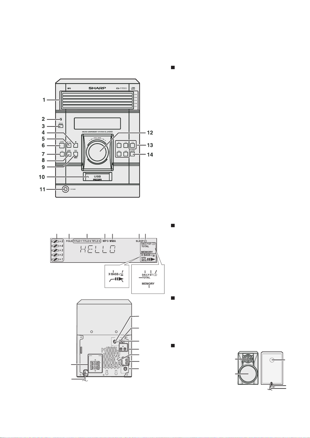
[3]
NAMES OF PARTS
XL-UH260
Controls and indicators
Front panel
1. Disc Trays
2. Timer Indicator
3. Remote Sensor
4. Disc or USB Stop Button
5. Disc or USB Play or Repeat Button
6. Power ON/STANDBY Button
7. CD Button
8. Tuner (Band) Button
9. Video/Auxiliary/USB Button
10. USB Terminal
11. Headphone Jack
12. Volume Control
13. Disc Number Select Buttons
14. Disc Tray Open/Close Button
12 3 45 67
13 14
9 10 11
8
15
16
12
3
4
ANTENNA
FM
GND
AM
75 OHMS
VIDEO/AUX I
RIGHTLEFT
SPEAKER
S
RATED SPEAKER IMPEDANCE
:
6 OHMS MIN
.
1
AC INPUT
RIGHT
LEFT
T
S
P
H
R
U
G
I
E
-
R
T
AK
H
E
G
FT
I
E
L
SP
L
R
E
T
F
U
O
OO
E
W
R
B
P
U
S
5
N
6
7
8
9
2
Display
1. Disc Number Indicators
2. MP3/WMA Folder Indicator
3. MP3/WMA Title Indicators
4. MP3 Indicator
5. WMA Indicator
6. Sleep Indicator
7. Timer Play Indicator
8. MP3/WMA Total Indicator
9. Daily Timer Indicator
10. FM Stereo Mode Indicator
11. FM Stereo Receiving Indicator
12. Memory Indicator
13. Extra Bass Indicator
14. Disc or USB Repeat Play Indicator
15. Disc or USB Pause Indicator
16. Disc or USB Play Indicator
Rear panel
1. Speaker Terminals
2. AC Power Cord
3. FM 75 Ohms Antenna Jack
4. AM Antenna Ground Terminal
5. AM Loop Antenna Terminal
6. Video/Auxiliary (Audio Signal) Input Jacks
7. Cooling Fan
8. Speaker Light-up Jacks
9. Subwoofer Pre-output Jack
Speaker system
1.Tweeter
2.Woofer
3.Bass Reflex Duct
4.
Speaker Light-up Wire
Speaker Wire 5.
1
2
3
4
5
1 – 5
1 – 3
Page 6
XL-UH260
1
11
7
12
8
13
2
9
14
15
16
17
18
10
19 20
3
2221
23 24
4
5
25
6
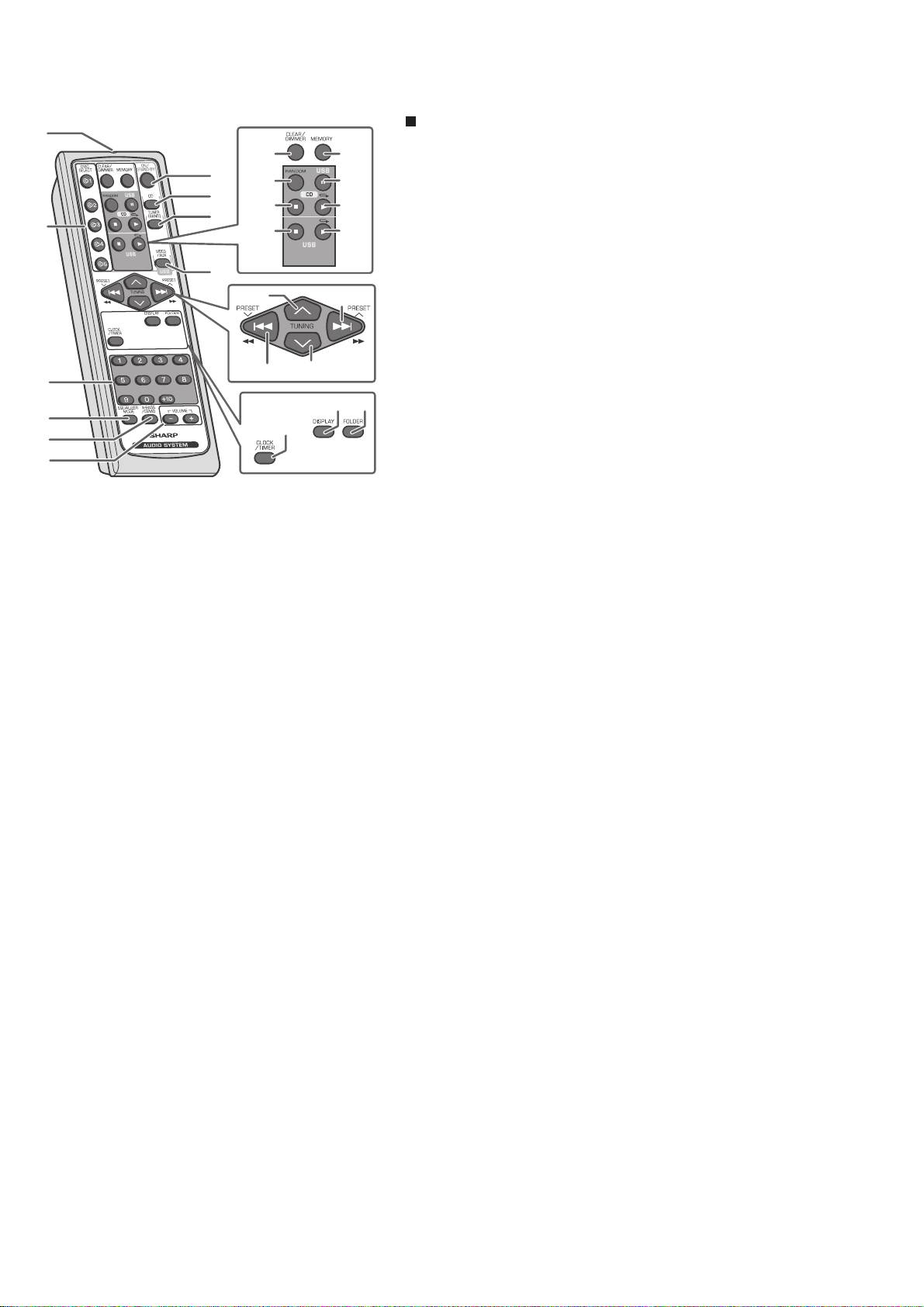
Remote control
1. Remote Control Transmitter
2. Disc Number Select Buttons
3. Disc Direct Search Buttons
4. Equalizer Mode Select Button
5. Extra Bass/Demo Button
6. Volume Up and Down Buttons
7. Power On/Stand-by Button
8. CD Button
9. Tuner (Band) Button
10. Video/Auxiliary/USB Button
11. Disc Clear/Dimmer Button
12. Disc Random Button
13. Disc Stop Button
14. USB Stop Button
15. Memory Button
16. Disc/USB Pause Button
17. Disc Play or Repeat Button
18. USB Play or Repeat Button
19. Tuning Up Button
20. CD Track Up or Fast Forward, Tuner Preset Up,
Time Up Button
21. CD Track Down or Fast Reverse, Tuner Preset Down,
Time Down Button
22. Tuning Down Button
23. Display Button
24. Folder Button
25. Clock/Timer Button
1 – 6
1 – 4
Page 7
CHAPTER 2. ADJUSTMENTS
[1] CD SECTION
1. CD SECTION
• Adjustment
Since this CD system incorporates the following auto-
matic adjustment functions, readjustment is not
needed when replacing the pickup. Therefore, different PWBs and pickups can be combined freely.
Each time a disc is changed, these adjustments are
performed automatically. Therefore, playback of each
disc can be performed under optimum conditions.
Items adjusted automatically
1) Offset adjustment (The offset voltage between the
head amplifier output and the VREF reference voltage is compensated inside the IC.)
* Focus offset adjustment
* Tracking offset adjustment
2) Tracking balance adjustment
3) Gain adjustment (The gain is compensated inside the
IC so that the loop gain at the gain crossover frequency will be 0 dB.)
* Focus gain adjustment
XL-UH260
* Tracking gain adjustment
2. CD ERROR CODE DESCRIPTION
Error Explanation
10* CAM error. Can't detect CAM switch when CAM is moving.
11* When it detect cam operation error during initialize process.
20* TRAY error. Can't detect TRAY switch when TRAY is mov-
ing.
21* When it detect TRAY operation error during initialize pro-
cess.
* 'CHECKING'
If Error is detected, 'CHECKING' will be displayed
instead of 'ER-CD**'. 'ER-CD**' display will only be
displayed when error had been detected for the 5
times.
th
2 – 1
Page 8
XL-UH260
[2] TEST MODE
• Setting the test mode
During stand-by mode, press STOP button while pres sing down the button and button. Then, press
3
the CD button to enter the test mode.
4
\
Step
Step
Step
Step
C DTEST
OPEN/CLOSE operation is using manual. IL isn’t done
/
1
2
3
4
<< >> key input.
Laser ON.
/
<< >> key input.
Focus ON
/
<< >> key input.
CLV Servo ON
/
<< >> key input.
Tracking Servo ON
IL isn’t done
Step
/
5
Hold down << CD >> key for more than 2 sec.
Start Auto Adjustment at current pick-up location.
<< >> key input.
Reading Sub-code and Display
<<STOP>> key input.
STOP and return to Step
<<STOP>> key input.
STOP and return to Step
Everytime << DISPLAY >> key input
1
1
2 – 2
Page 9
a) Focus Balance = FB : XX
b) Focus Gain = FG : XX
c) Tracking Balance = TB : XX
d) Tracking Gain = TG : XX
e) Focus Offset = FOFF : XX
f) Tracking Offset = TOFF : XX
g) RFRP = RFRP : XX
h) Focus Error
(RW Judgement) = RW : XX - XX =XX
i) Focus Error
(Other than RW Judgement) = DA : XX - XX =XX
<<STOP>> key input.
XL-UH260
STOP and return to Step
Note
Sliding the PICKUP with<< >>, << >> button can be set
in STOP mode or play mode.
During at Step , if press << >> for more than 1 sec, it directly
goes to step .
To cancel: Power OFF
1
5
/
1
2 – 3
Page 10
XL-UH260
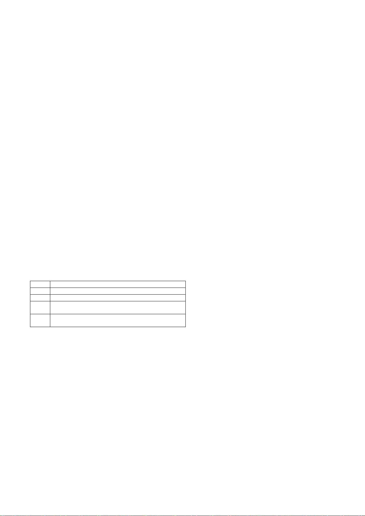
[3] Standard Specification of Stereo System Error Message Display Contents
Error Contents DISPLAY Notes
CD CD Changer Mechanism Error. ‘ER-CD**’ (*) 10: CAM SW Detection NG during normal operation
11: CAM SW Detection NG during initialize process
20: TRAY SW Detection NG during normal operation
21: TRAY SW Detection NG during initialize process
Focus Not Match/IL Time Over. ‘NO DISC’
TUNER PLL Unlock.
87.50
FM MHz
(*) CHECKING:
If CD changer mechanism error is detected, 'CHECKING' will be display instead of 'ER-CD**'. 'ER-CD**' display will only
be display when error had been detected for the 5
th
times.
Speaker abnormal detection and +B PROTECTION display
In case speaker abnormal detection or +B PROTECTION had occurred, the unit will automatically enter to stand-by
mode and Timer indicator will flashing as below.
Example:In case of speaker abnormal
PLL Unlock.
ON
FLASHING FLASHING
ON ON ON
TIMER
LED OFF OFF
NO NO. 1.1
NO. 2
1
FRAME
OFF
OFF OFF OFF OFF
NO. 2
(REPEAT)
NO. 1 : +B PROTECTION
NO. 2 : Speaker abnormal
BEFORE TRANSPORTING THE UNIT
The following process need to be taken after set tapering/parts replacement.
1. Press the POWER ON/STAND-BY button to enter stand-b y mode.
2. While pressing down the button and the button, press the button. The Micro Computer version number
3
4
will be displayed as
"XL-U-****” and " FW****_V**”.
3. Turn the VOLUME KNOB until FL will display “INIT_ _MENU.”
4. Press the button until "WAIT"--> "FINISHED" appears.
5. Unplug the AC cord and the unit is ready for transporting.
2 – 4
Page 11
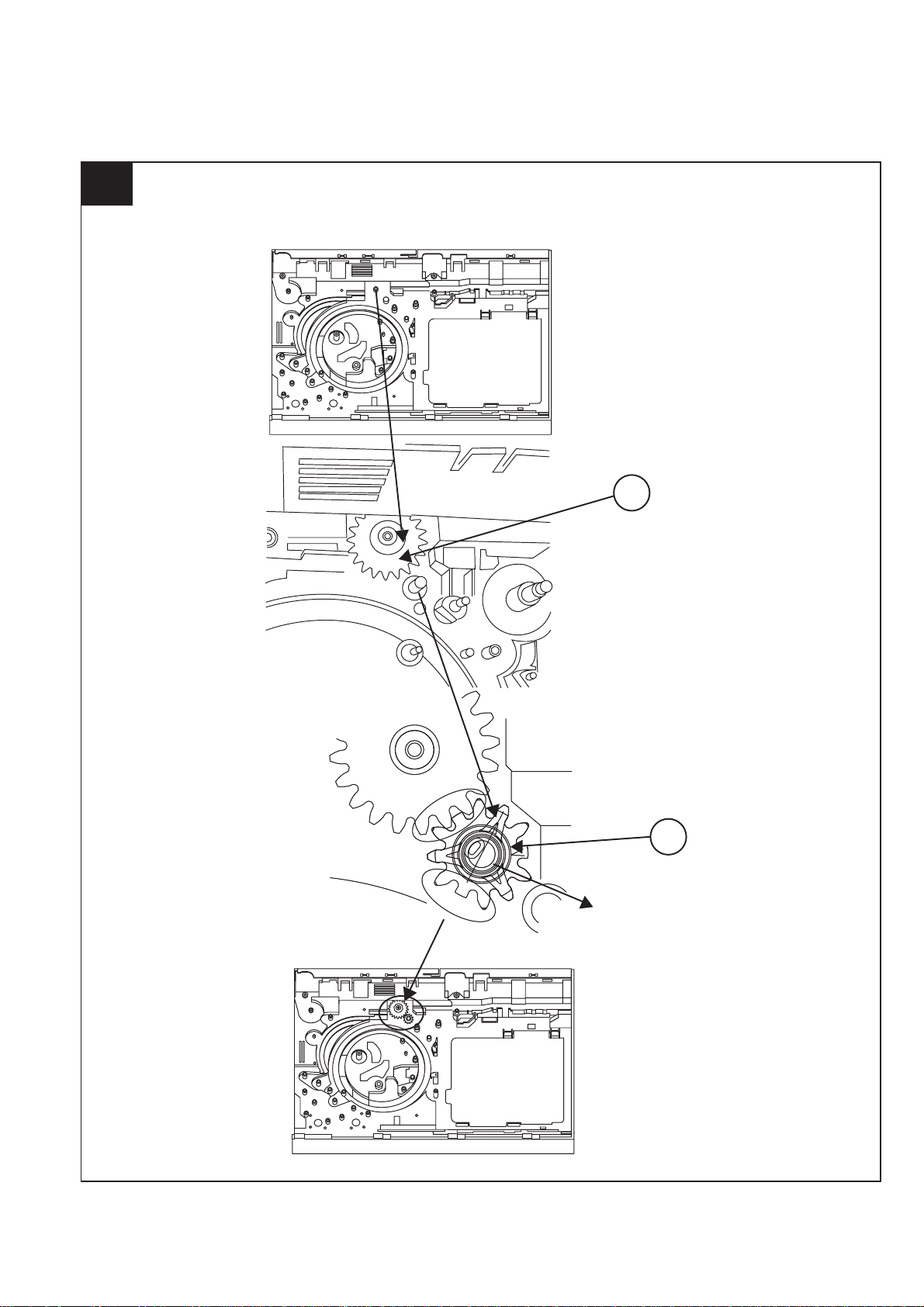
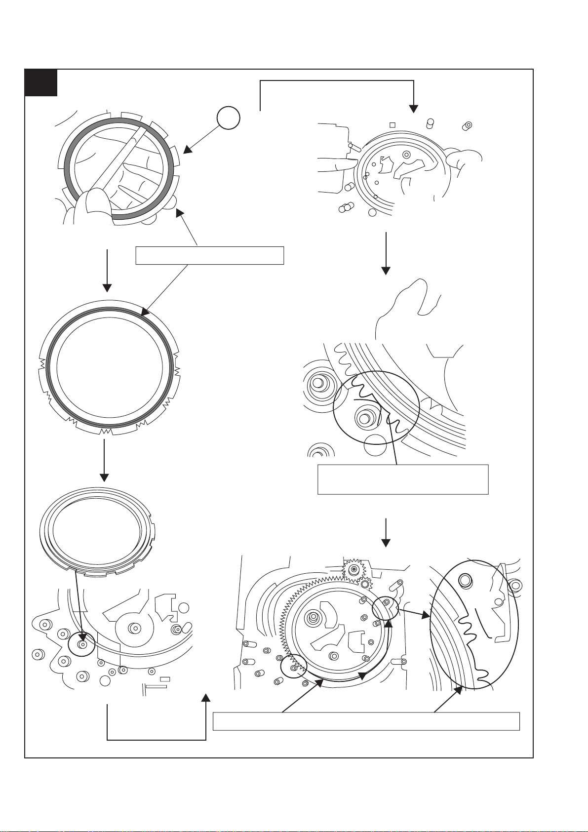
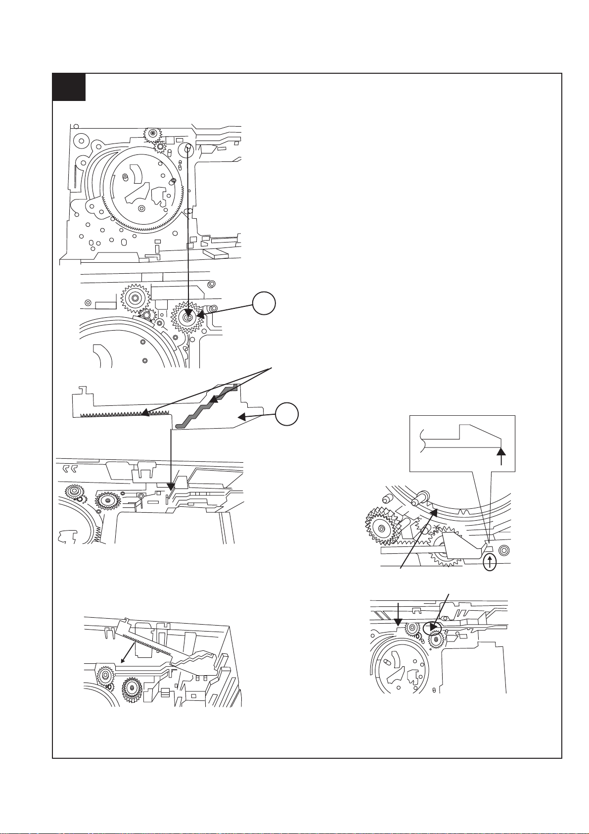
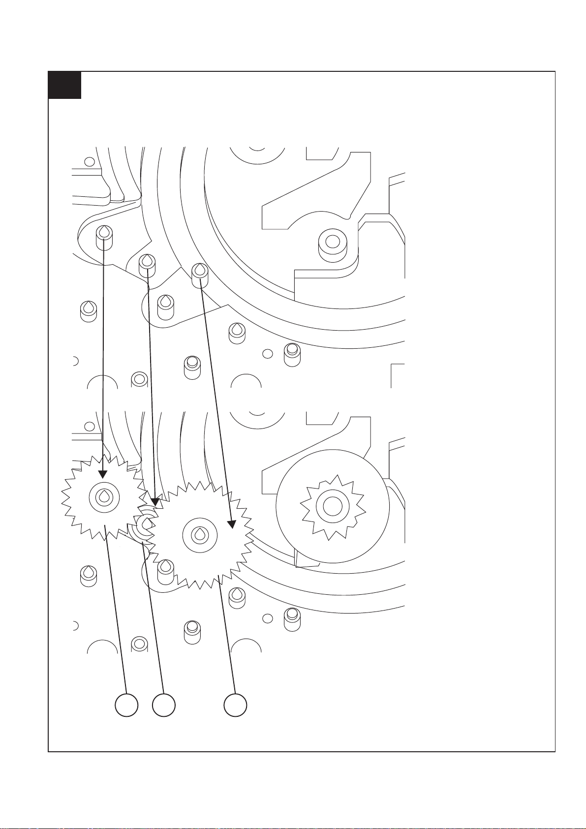
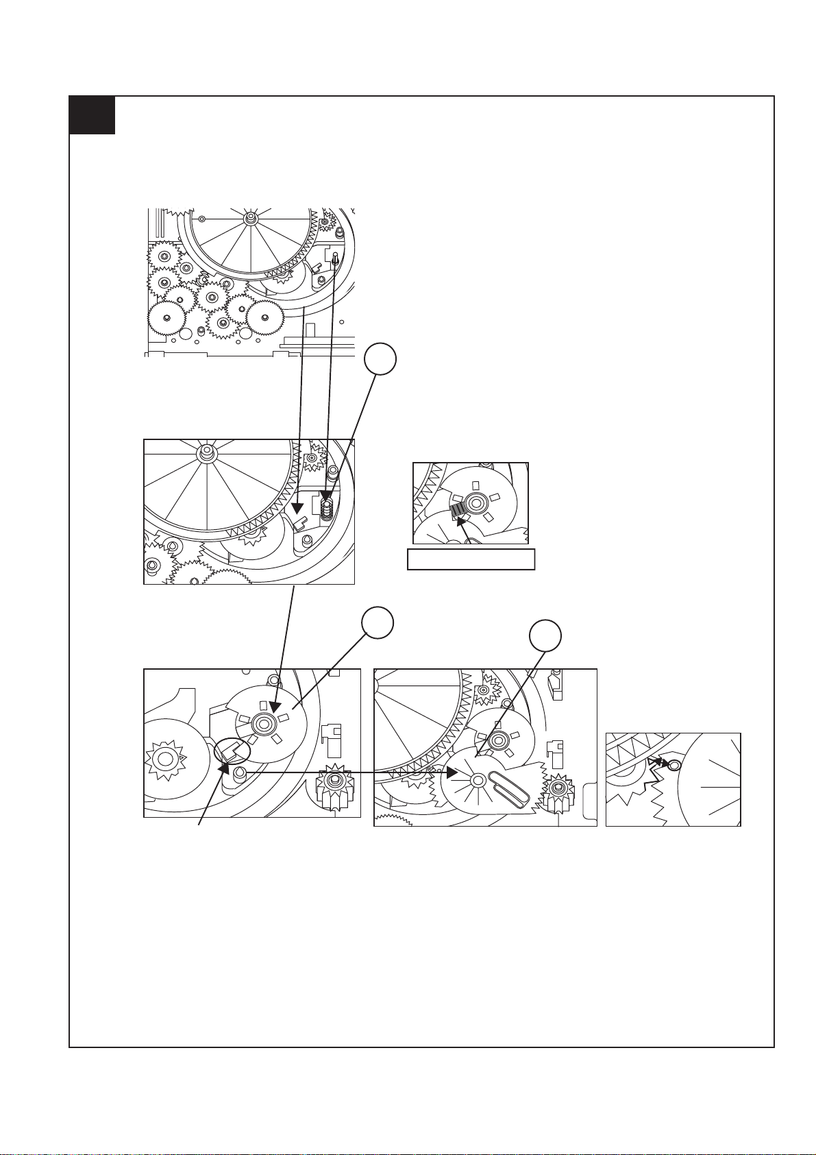
[4] CD Changer mechanism section
• All numbers in the drawing correspond to those in parts guide (CHANGER MECHANISM PARTS).
1
141
XL-UH260
2 – 5
140
HALF GEAR
MUST BE ARRANGED AS SHOWN
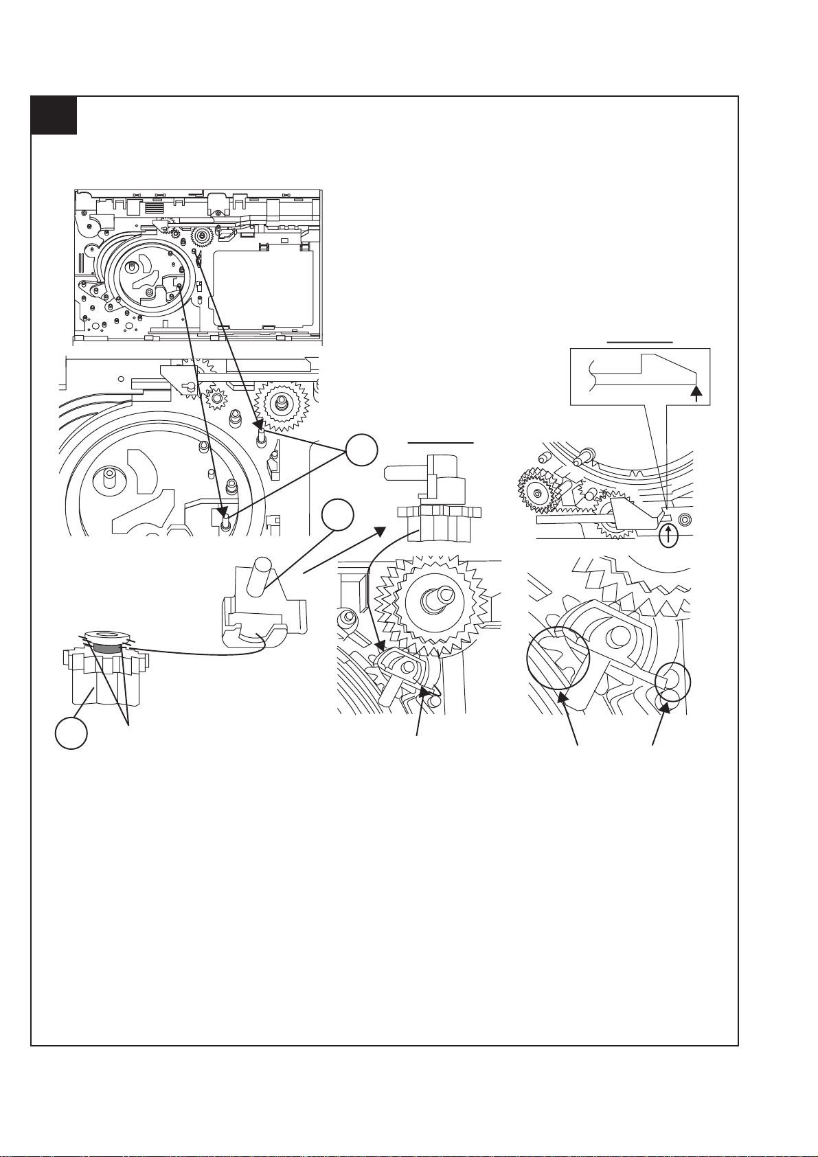
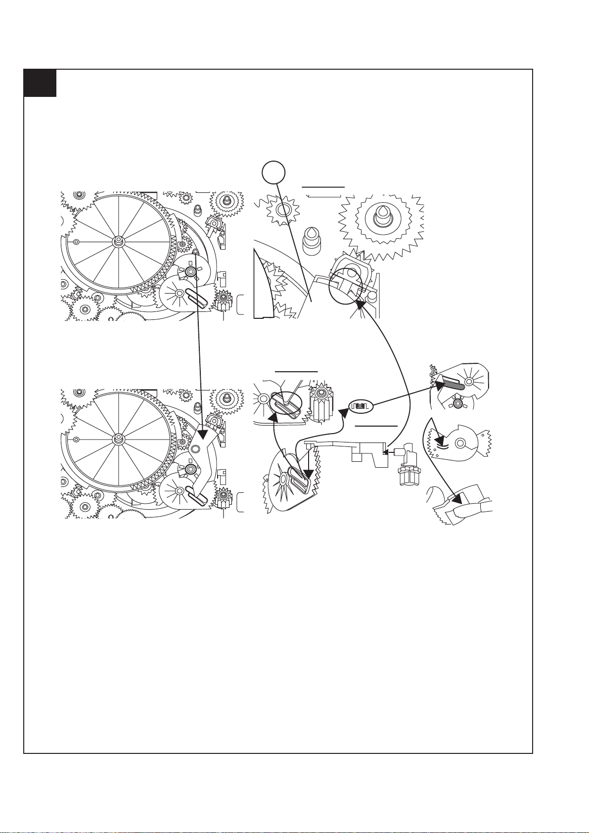
Page 12
XL-UH260
2
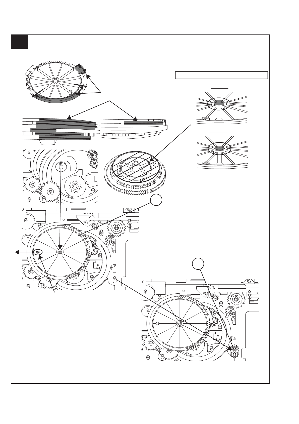
139
APPLY SANKOL SHS1001 BEFORE FIX
FIX ITEM 139 ACCORDING TO THE
PICTURE AS SHOWN ABOVE
ROTATE MODE BIG GEAR UNTIL REACH AS SHOWN IN PICTURE
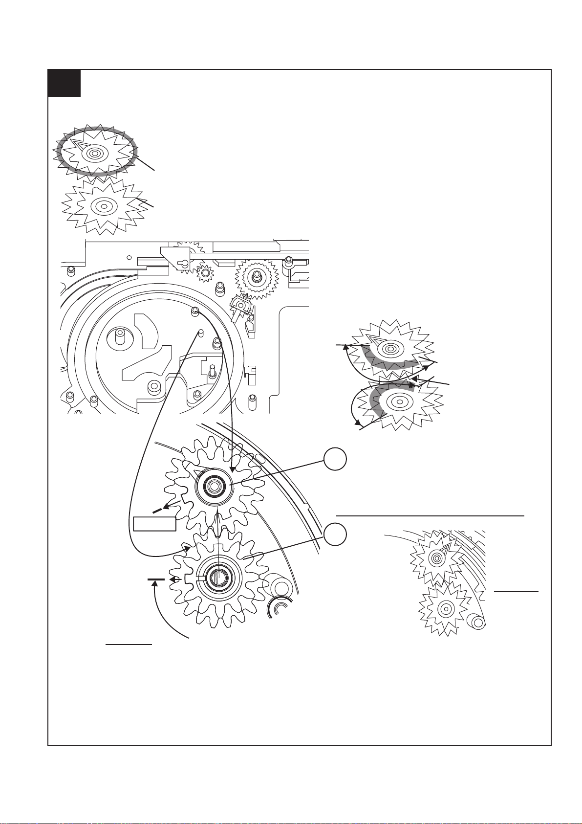
2 – 6
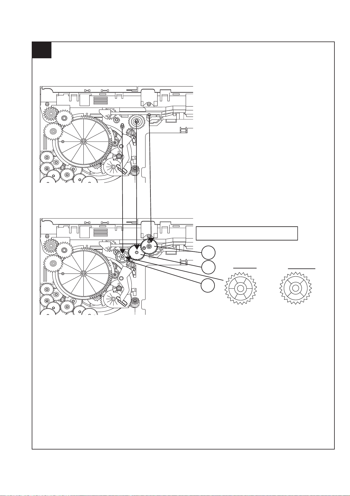
Page 13
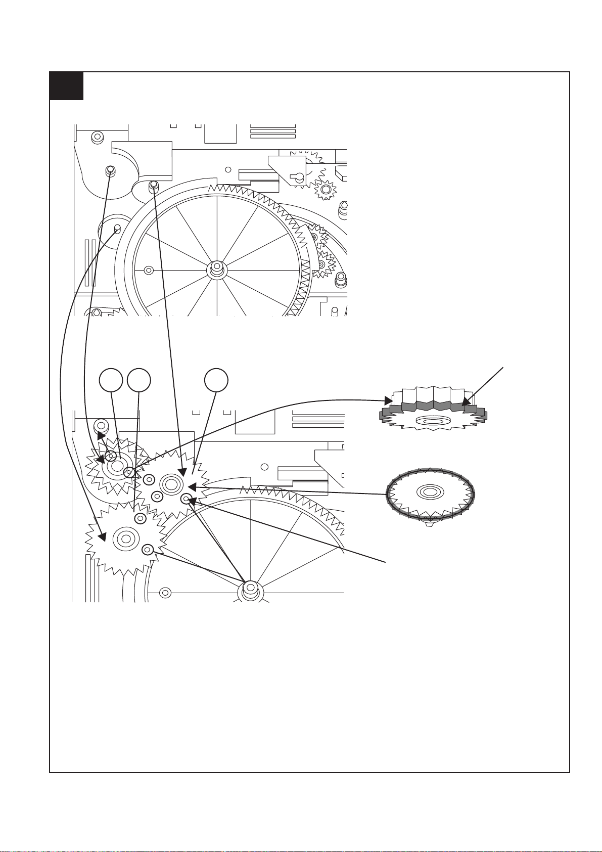
3
XL-UH260
143
APPLY GREASE SC141
112
PULL THE LEVER UNITIL
REACH THE ARROW MARK
2 – 7
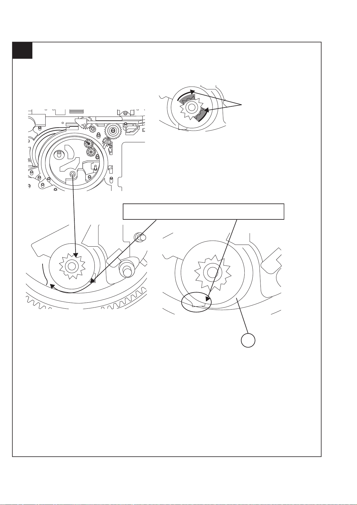
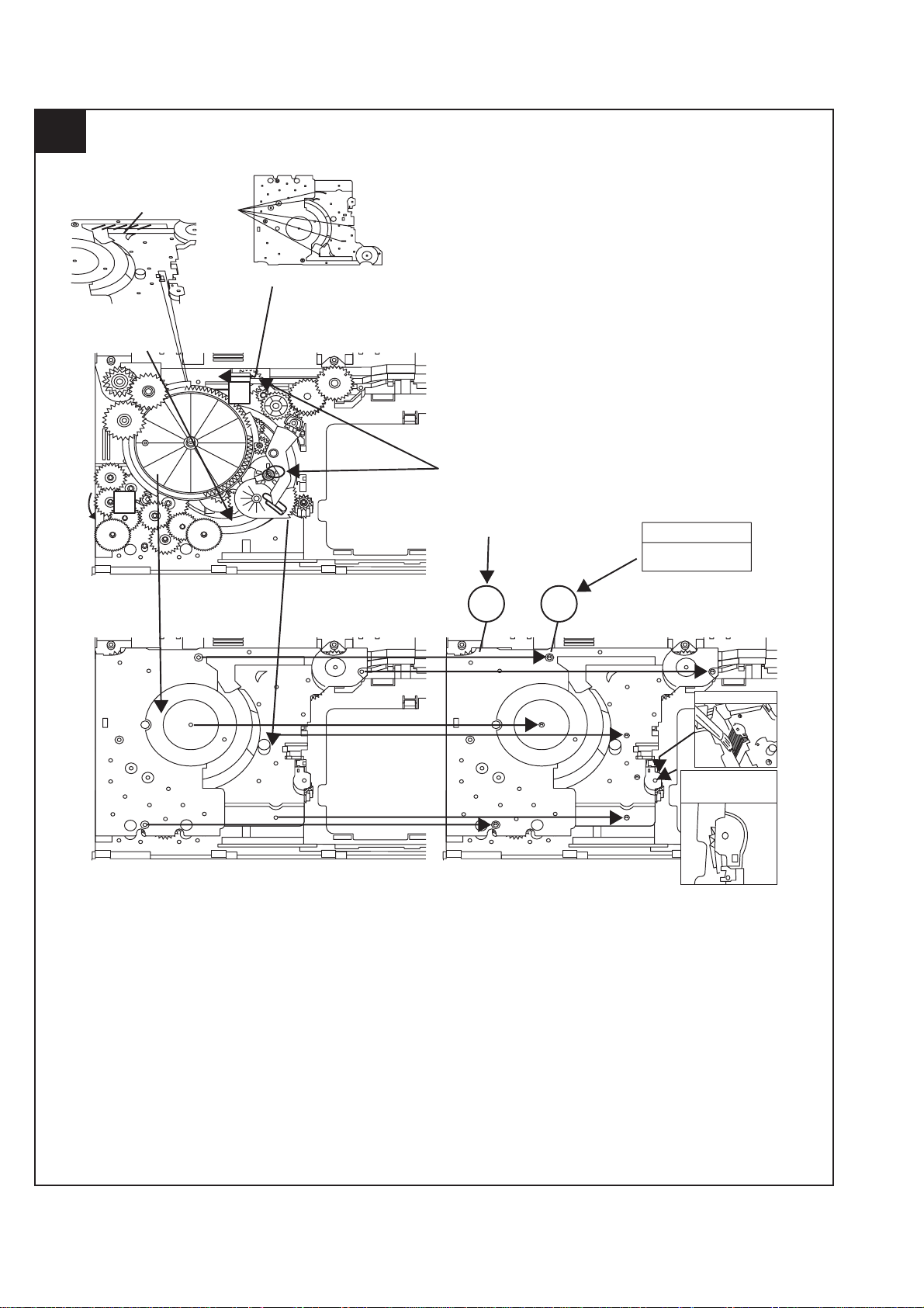
Page 14
XL-UH260
4
FIGURE 2
FIGURE 1
152
142
APPLY GREASE SC141
118
SLOT CLAMP
SWITCH ARM INSIDE BASE SLOT
HALF GEAR MUST BE
ARRANGED AS SHOWN
2 – 8
Page 15
5
XL-UH260
APPLY GREASE SC141 AT BOTTOM SIDE
OF GEAR FOLLOW MARKING (REFER TO GRAY AREA)
NO NEED TO APPLY GREASE AT BOTTOM
SIDE
FIGURE 1
APPLY GREASE SC141
AT TOP SIDE OF GEAR
FOLLOW MARKING
(REFER TO GRAY AREA)
127
IF DIRECTION IS OTHER THAN DIRECTION
SHOWN IN FIGURE 1, IT IS INCORRECT
CORRECT
128
INCORRECT
BLACK MARK
2 – 9
Page 16
XL-UH260
6
APPLY GREASE SC141
AT HALF GEAR AREA
ROTATE CLOCKWISE UNTIL REACH HERE (MAXIMUM)
129
2 – 10
Page 17
7
XL-UH260
151150149
2 – 11
Page 18
XL-UH260
8
THE SHOWN AREAMUST FREE FROM GREASE
CORRECT
GREASE SC141 APPLICATION LENGTH
GREASE APPLICATION PORTION
INCORRECT
SHOWN HOLE MUST FACING ARROW DIRECTION
124
131
2 – 12
Page 19
9
138
126
125
XL-UH260
APPLY GREASE SC141
AT BOTTOM SIDE
ONLY
TR-RE JOINT GEAR C
2 – 13
APPLY GREASE SC141 ONLY AT TOP SIDE GEAR
MUST BE FIXED ACCORDINGLY TO
THE HOLE'S
Page 20
XL-UH260
10
148
147
146
145
2 – 14
Page 21
11
XL-UH260
121
144
WHEN FIXING ITEM 144 MUST FOLLOW AS SHOWN
APPLY GREASE SC141
130
2 – 15
Page 22
XL-UH260
12
117
FIGURE 2
FIGURE 1
APPLY GREASE
SC141
FIGURE 3
APPLY GREASE SC141
2 – 16
Page 23
13
XL-UH260
ITEM 133 , 134 MUST APPLY GREASE SC141
ON TOP SIDE GEAR ONLY
134
GEAR 112 GEAR 112
133
132
CORRECT
TOP VIEW AFTER
BEING ASSEMBLED
INCORRECT
IT IS INCORRECT TO
FIX IT IN REVERSED
DIRECTION
2 – 17
Page 24
XL-UH260
14
APPLY GREASE SC141
BEFORE FIX
MOVE 112 UNTIL TOUCH THE WALL
B
DURING GEAR A ROTATE
MUST PRESS SHOWN AREA
A
AND LEVER B WILL MOVE
ARROW DIRECTION THEN
FIX PART 108
SCREW TORQUE
+0.5
2 kgf-cm
-0
108
803 x6
APPLY GREASE SC141
CONFIRM WHETHER
FIXED
PROPELY OR NOT
2 – 18
Page 25
15
XL-UH260
APPLY GREASE SC141
113
BEHIND THE LEVER NEED TO APPLY GREASE SC141
PULL IT THEN LEVER WILL
MOVE IN
2 – 19
Page 26
XL-UH260
16
123
115
APPLY GREASE SC141
APPLY GREASE SC141 BEFORE FIX
APPLY GREASE
SC141 AT BOSS
SPRING MUST BE ARRANGED UNDER THE HOOK
BOARD R
BOARD R
LR JOINT LEV
LR JOINT LEV
2 – 20
Page 27
17
XL-UH260
IT IS INCORRECT IF ASSEMBLED IN
A REVERSED DIRECTION
103
137
136
APPLY GREASE SC141
BIG SLOT MUST FACING OUT
WHEN FIX AND AFTER FIXED TO BASE CHASSIS.
AFTER ASSEMBLY, CONFIRM WITH FREE DROP TEST
GEAR POSITION DURING FIXING
2 – 21
Page 28
XL-UH260
18
IT IS INCORRECT IF ASSEMBLED IN
A REVERSED DIRECTION
APPLY GREASE SC141
104
135
136
BIG SLOT MUST FACING OUT
WHEN FIX AND AFTER FIXED TO BASE CHASSIS
AFTER ASSEMBLY, CONFIRM WITH FREE DROP TEST
GEAR POSITION DURING FIXING
CONFIRM BOTH GEARS SIT PROPERLY AND LOCKED
2 – 22
Page 29
19
XL-UH260
AFTER FIX OUTER UP/DOWN LEVER HOLD AS SHOWN PORTION AND
MOVE UP/DOWN THEN CONFIRM WHETHER LEVER GO INSIDE THE
HOLE OR NOT
120
137
119
BIGGER SLOT FACING OUT
135
BIGGER SLOT FACING OUT
IT IS CORRECT IF THE LEVER HOLD
ENTERS THE HOLE
IT IS INCORRECT IF THE LEVER HOLD DOES NOT
ENTER THE HOLE
ALL OF THIS 135 AND 137 GEAR FIX TOGETHER WITH 119
AND 120 LEVER ( MOVE TOGETHER )
2 – 23
Page 30
XL-UH260
20
BIGSLOTFACINGOUT
110
2 – 24
Page 31

21
XL-UH260
PUSH THE LEVER ACCORDING TO ARROW
DIRECTION THEN FIX
WHEN FIXING MAIN BASE ASSEMBLY FOLLOW ACCORDING TO PICTURE 1
PICTURE 1
CORRECT INCORRECT INCORRECT
MAKE SURE MECHA HOLDER SHAFT FIX PROPERLY TO LEVER
PICTURE 3
PICTURE 2
2 – 25
Page 32

XL-UH260
22
APPLY SANKOL (SHS1001)
101
102
APPLY SANKOL
(SHS1001) ON TOP
APPLY SANKOL (SHS1001) INSIDE
THE SLOT & OTHER SHOWN PORTION
APPLY SANKOL
(SHS1001)
APPLY SANKOL (SHS1001) AT
TRAY SLIDING PORTION
FIX TRAY NO 1 FIRST THAN
FOLLOW OTHER
APPLY SANKOL (SHS1001) AT BACK PORTION
COSMO GUIDE TRAY HAVE
MARKING AS SHOWN
2 – 26
Page 33

23
GEAR UP/DOWN BOARD
111
APPLY GREASE SC141 AT INNER & OUTER GEAR SLIDING PORTION
WHEN FIX GEAR UP/
DOWN BOARD THE
TWO LEVER MUST AT
PARALLEL LINE AND
POSITIONED AT TOP
MAX SIDE
XL-UH260
2 – 27
AFTER ASSEMBLY GEAR UP/DOWN BOARD
Page 34

XL-UH260
24
SCREW TORQUE
+0.5
3 kgf-cm
-0
ROTATE THE GEAR TO MOVE UP 111 GEAR
UP AND DOWN BOARD BEFORE SCREW
804
2 – 28
Page 35

25
XL-UH260
AFTER ASSEMBLY TOP PLATE
FIX THE FFC
FFC4
AFTER PUSH, MAKE SURE SNAP PROPERLY
AFTER FIX, PUSH FOLLOW ARROW DIRECTION
BEFORE LOCK
AFTER LOCK
BACK
PORTION
107
122
BEFORE LOCK
PRESS IN
SLOT IN
BEFORE LOCK
AFTER LOCK
AFTER LOCK
MUST CONFIRM
MUST CONFIRM
2 – 29
Page 36

XL-UH260
26
CORRECT
INCORRECT
CAUTION
1. MAKE SURE NO PWB CHIP INSIDE SET .( BEFORE FIX MAKE
SURE PWB IS FREE FROM DUST , GREASE & ETC )
803
2 – 30
Page 37

27
APPLY GREASE SC141
THE TWO SLOT MUST FREE
FROM GREASE SC141
APPLY GREASE SC141
BELOW THE MARKING
FOR BOTH PORTION
XL-UH260
ASSEMBLY SEQUENCE
1. APPLY GREASE SC141 TO MAIN BASE
GREASE SC141 APPLICATION AREA
ALL BOSS
APPLY GREASE
SC141
CAUTION
TRAY SLIDING
AREA MUST
FREE FROM
GREASE SC141
APPLY GREASE
SC141
APPLY GREASE
APPLY GREASE SC141 AT WALL
APPLY GREASE
SC141
SC141
105
APPLY GREASE SC141
AT BOTH SLOT
APPLY GREASE SC141 AT 3 HALF MOON
1 RIB ONLY
APPLY GREASE
SC141
APPLY GREASE SC141
INSIDE SLOT
2 – 31
Page 38

XL-UH260
28
REFERENCE ONLY
MOTOR GEAR HEIGHT FROM
MAIN BASE 12.2
+
0.1
-
0.1
-
+
12.2
MOTOR SCREWING HOLE
MUST HAVE GAP
M1,2
801
-0
13.8 + 0.2
APPLY GREASE SC141
SCREW TORQUE
1.5 + 0.5
-0
AFTER SCREW MOTOR, CONFIRM THE
ARRANGEMENT AS IN FIGURE 2
FIGURE 2
2 – 32
Page 39

29
APPLY SANKOL (SHS1001)
XL-UH260
3.1 + 0.1
SHAFT X 3 DIM AFTER INSERTION
MUST CONFIRM EVERYDAY
109-2
APPLY GREASE AT THE SLIDING PORTION
114
116
UP / DOWN
HOLDER CHANGE
TO NATURE
COLOR
SANKOL
APPLICATION AREA
(SHS1001)
APPLY GREASE SC141
2 – 33
Page 40

XL-UH260
30
BEFORE MELT IT
AFTER MELT IT ( MUST FLAT )
WHEN FITTING STABILIZER PLATE TO STABILIZER,
ROTATE STABILIZER ANTI CLOCKWISE BY JIG
( STRICTLY CANNOT FIT USING HAND)
( BY HAND CANNOT X )
BELOW
AFTER ASSEMBLED TO
HOLDER, STABILIZER
NEED TO BE CLEANED
WITH ALCOHOL DISC
TOUCHING SURFACE
2 – 34
Page 41

31
XL-UH260
106
APPLY GREASE SC141
MUST MAKE SURE SNAP PROPERLY BOTH SIDE
ALL SURFACE MUST TOUCH
CORRECT INCORRECT
GAP
INCORRECT
2 – 35
Page 42

XL-UH260
32
NO GAP HAVE GAP
CORRECT INCORRECT
2 – 36
Page 43

XL-UH260
CHAPTER 3.
MECHANICAL DESCRIPTION
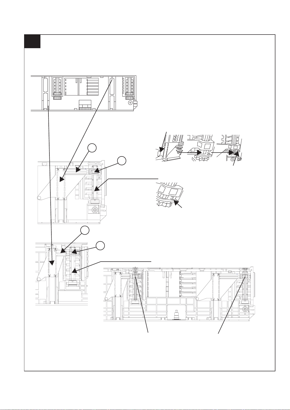
[1] REMOVING AND REINSTALLING THE MAIN PARTS
1. CD MECHANISM SECTION
Perform steps 1, 2, 9, 10, 11 and 12 of the disassembly
method to remove the CD mechanism.
1.1. Remove the pickup. (See Fig. 1)
1. Remove the stop washer (A1) x 1 pc., to remove the gear
(A2) x 1 pc.
2. Remove the screws (A3) x 2 pcs., to remove the shaft
(A4) x 1 pc.
3. Remove the pickup.
Note
After removing the connector for the optical pickup from
the connector wrap the conductive aluminium foil around
the front end of connector so as to protect the optical
pickup from electrostatic damage.
(A3)x2
φ2.6x6mm
2.1. How to remove CD Disc (See Fig. 2~5)
1. When CD is at play position (Figure 2), rotate reduction
gear C clock-wise as shown in Figure 3 Until disc tray
is at stock position, then rotate further to eject the disc
tray so that CD can be removed from the tray.
CD Disc
Disc Tray
Guide Tray
CD At play position.
CD Disc
CD Mechanism
Shaft
(A4)x1
Gear
(A2)x1
Stop Washer
(A1)x1
Pickup Unit
Figure 1
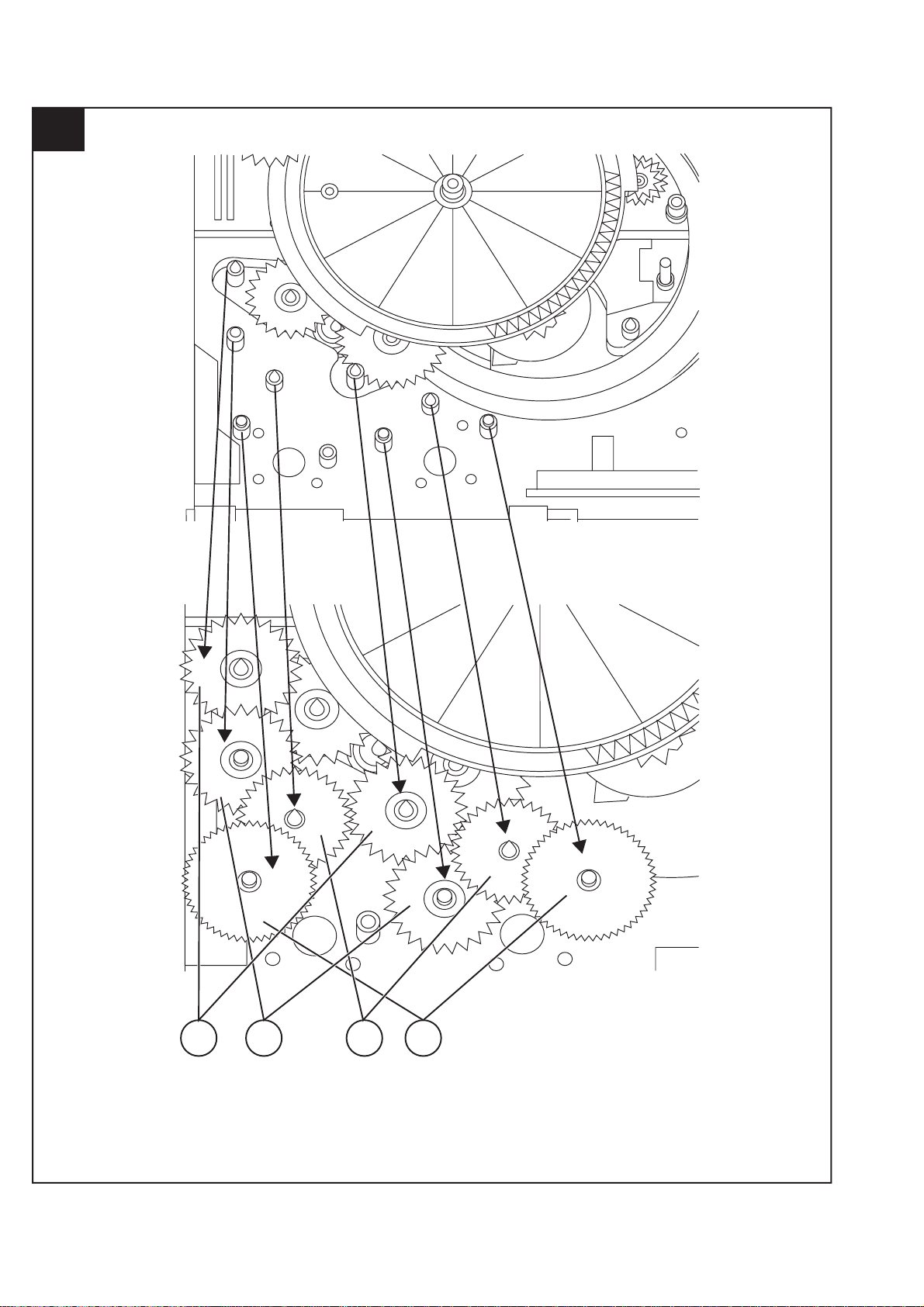
2. CHANGER MECHANISM SECTION
Perform steps 1, 2, 9 and 10 of the disassembly method to
remove the CD changer mechanism.
CD At stalk position.
Figure 2
Reduction gear C
Front Rear
Figure 3
2. In another case, if CD mechanism is at tray No.1 play
position and to remove CD located in tray No.3, the
procedure is as follows:
If the gear up down board is located at tray No.1 position,
then rotate gear clock-wise until it at stock position.
Rotate reduction gear D clockwise (Figure 4) to move the
CD mechanism to tray No.3 position.This is confirmed by
checking the gear up down board position by the marking
as indicated on the main chassis as shown in Figure 5.
3 – 1
Page 44

XL-UH260
Reduction gear D
Up Down
Figure 4
Gear up down board
Mark 1
(DISC 1)
Mark 3 Mark 5
(DISC 3)
Mark 2 Mark4
(DISC 2)
(DISC 4)
(DISC 5)
Figure 5
2.2. How to Remove the tray motor/main cam motor/5Changer Motor PWB (See Fig. 1)
1.Remove the screws (A1)x 2 pcs., to remove tray motor/main cam
motor/5-Changer Motor PWB.
Changer Mechanism Unit
Main Cam Motor
(A1)X2
φ2x10mm
Tray Motor
5-Changer
Motor PWB
Figure 1
NOTE:There are 2 more screws tighten the motors at the bottom of
main chassis. Before performing procedure 1 above, disc stop
spring, top plate sear up down board and trays must be
removed, then only the 2 screws can be untighten.
3 – 2
Page 45

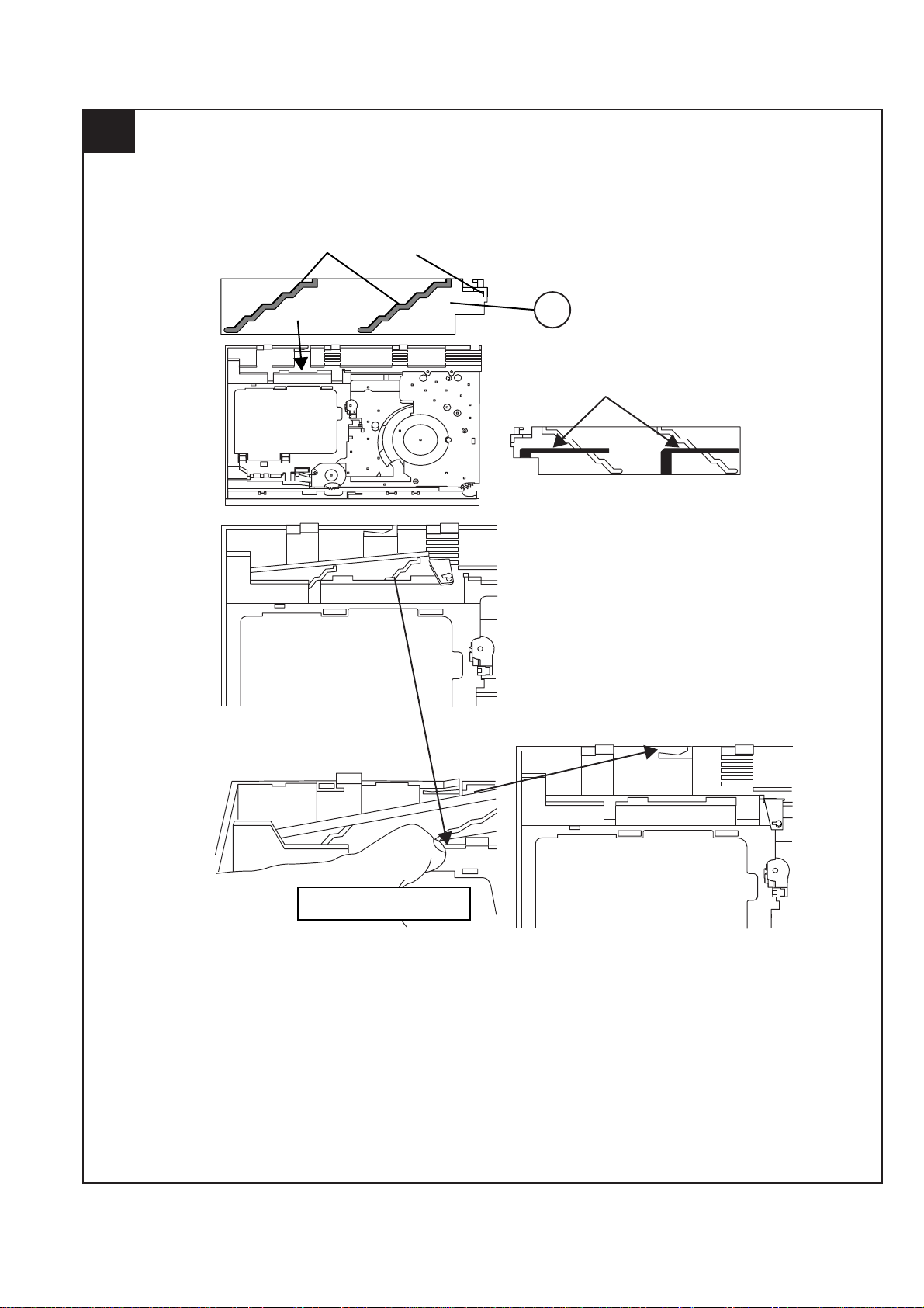
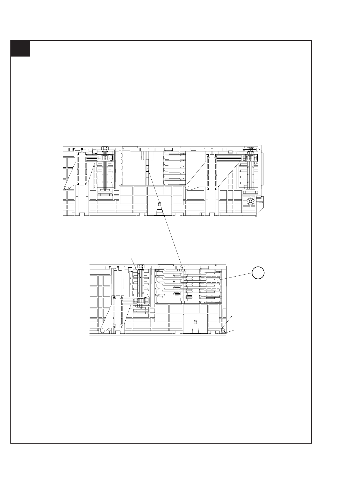
[2] DISASSEMBLY
XL-UH260
Caution on disassembly
Follow the below-mentioned notes when disassembling
the unit and reassembling it, to keep it safe and ensure
excellent performance:
1) Take cassette tape and compact disc out of the unit.
2) Be sure to remove the power supply plug from the
wall outlet before starting to disassemble the unit.
3) Take off nylon bands or wire holders where they
need to be removed when disassembling the unit.
After servicing the unit, be sure to rearrange the
leads where they were before disassembling.
4) Take sufficient care on static electricity of integrated
circuits and other circuits when servicing.
STEP REMOVAL PROCEDURE FIGURE
1 Top Cabinet 1. Screw…………..……….(A1) X 6 1
2 Side Panel (Left/ 2. Screw……….…………..(B1) X 8 1
Right)
3 CD Changer unit 1. Screw…………..……….(C1) X 2 2
2. Hook ……………………(C2) X 2
3. Socket………………..…(C3) X 2
4. Flat Cable ……… …….(C4) X 2
4 Rear Panel with 1. Screw………..………….(D1) X 2
Speaker PWB and
Refresh PWB
2. Socket………………..…(D2) X 1
3. Flat Cable ……… …….(D3) X 1
4
5 Front Panel 1. Screw………………..….(E1) X 2 3
2. Flat Cable ………..…….(E2) X 2
3. Socket……..……………(E3) X 1
4. Hook …………….…...…(E4) X 2
6 Main PWB 1. Screw………………..….(F1) X 4 3
2. Socket……..……………(F2) X 2
7 Power PWB 1. Screw………………..….(G1) X 4 3
8 Speaker PWB 1. Screw…….…………..….(H1) X 2 4
9 Refresh PWB 1. Screw…….…………..….(J1) X 1 4
10 Display PWB
1. Knob……..…………..….(K1) X 1
2. Nut…………....……..…..(K2) X 1
5
3. Washer…………....…….(K3) X 1
4. Screw…………....……...(K4) X 6
11 USB PWB 1. Screw………………..….(L1) X 2 5
12 Jack PWB 1. Screw………………..….(M1) X 1 5
13 CD MP3 PWB 1. Screw…….………….….(N1) X 2 6
2. Flat Cable ………..…….(N2) X 2
3. Socket……..……………(N3) X 1
14 CD Mechanism 1. Screw…….………….….(P1) X 4 6
2. Changer Chassis……….(P2)X 4
7
Note:
After removing the connector for the optical pickup from
the connector, wrap the conductive aluminium foil around
the front end of the connector so as to protect the optical
pickup from electrostatic damage.
(A1)x2
3x12mm
(B1)x2
3x10mm
Side Panel
(Right)
(A1)x2
3x12mm
(B1)x2
3x10mm
Rear Panel
CD Changer Unit
Refresh PWB
Rear Panel
Speaker PWB
Power PWB
(B1)x2
3x10mm
(D1)x4
3x10mm
(E4)x1
(F2)x1
(G1)x4
4x6mm
Top Cabinet
Figure 1
CD Servo PWB
Figure 2
PULL
Figure 3
(F1)x2
3x6mm
(E3)x1
Main PWB
(B1)x2
3x10mm
PULL
(C1)x1
3x10mm
Hook
(C2)x1
(F1)x2
3x10mm
(C4)x2
Front Panel
(C3)x2
Front panel
(F2)x1
Side Panel
(Left)
Front Panel
(D2)x1
(E1)x2
3x10mm
(D3)x1
PULL
(A1)x2
3x12mm
Hook
(C2)x1
PULL
(C1)x1
3x10mm
(E2)x2
Hook
(E4)x1
3 – 3
Page 46

XL-UH260
Refresh PWB
Speaker PWB
(K4)x6
2.6x10mm
Rear Panel
Display PWB
USB PWB
Figure 4
Front Panel
(J1)x1
3x10mm
(K2)x1
(K3)x1
(H1)x2
3x10mm
(K1)x1
(P2)x4
Special
CD Mechanism
CD Changer Unit
Figure 7
STEP PROCEDURE FIGURE
1 Woofer 1. Front Panel………….…..(A1) X 1
2 Tweeter 1. Screw…….……….....….(B1) X 2
REMOVAL
8
2. Socket…….…….…….…(A2) X 1
3. Screw…….…….…….….(A3) X 2
4. Screw…….…….…….….(A4) X 4
(L1)x2
2.6x10mm
Figure 5
CD Changer
Unit
(P1)x2
3x10mm
Jack PWB
(M1)x1
Special
(N1)x2
(N2)x2
(P1)x2
3x10mm
(N3)x1
Front Panel
(A1)x1
(B1)x2
3x10mm
TWEETER
WOOFER
(A4)x4
4x16mm
(A2)x1
LED PWB
LED PWB
Figure 8
Speaker Box
(A3)x2
Ø3x10mm
Screwdriver
Figure 6
3 – 4
Page 47

-MEMO-
XL-UH260
3 – 5
Page 48

XL-UH260
CHAPTER 4. BLOCK DIAGRAM
A
B
C
D
E
F
G
H
1
23456
Figure 1: CD MP3 BLOCK DIAGRAM (1/2)
4 – 1
Page 49

XL-UH260
7
8 9 10 11 12
Figure 2: CD MP3 BLOCK DIAGRAM (2/2)
4 – 2
Page 50

XL-UH260
T
A
AC_RLY
SPK_DET
LED708
BI703
CNP703
B
C
D
E
F
G
H
NC
+B2
CNP301
L
R
JK690
FROM
CD/MP3 SECTION
CHASSIS_GND
FM_DET
TUN_SM
R_CH
+9V
L_CH
CHASSIS_GND
DO
CL
DI
CE
CNP601
1
2
3
4
TO CD/MP3
VIDEO/AUX
TUNER
CNP601
SECTION
L
R
L
R
AUDIO PROCESSOR
L
R
8.5V
+B1
+B3
9
8
7
6
5
+B_PROTECT
SERVO_+5V
+B4
SW_+5V
TUNER PACK UNIT
RTUNSA007AWZZ
DI
IC601
CE
CLK
LC75341
+B2
10V
+B2
13V
Q860
+B7
A_5V
SP_DE
VH+
VLVL+
IC704
VOLTAGE
REGULATOR
L_OUT
R_OUT
VH-
D801
D802
Q901
Q904
F802
4A 125V
F801
4A 125V
F804
2A 125V
F803
2A 125V
Q801
D842-D845
+B4
(SW_+5V)
TUN_SM/SPAN
-20DB_ATT
P_IN
VL-
R
L
Q601
Q602
Q603
Q604
UNSW_5.6V
+B9
8.5V
10V
13V
5.1V
VL+
IC851
AN80T53
VOLTAGE
REGULATOR
-VF
VF2
VF1
IC852
7805
VOLTAGE
REGULATOR
IC854
78L05
VOLTAGE
REGULATOR
Q841
1
23456
Figure 3: MAIN, DISPLAY & POWER BLOCK DIAGRAM (1/2)
4 – 3
Page 51

BI703
SP_DET
CNP703
+B2
VR701
JOG
VOLUME
Q706
XL-UH260
FL701
+B
+B8
FL DISPLAY
IC701
DRIVER IC
+B9
VF1
-VP
LED707
Q705
PHOTO
DO
CL
DI
CE
A_+10V
Q704
TO CD/
MP3 SECTION
IC702
GND
VF2
TIMER
LED
+B8
VCC
+B8
F802
4A 125V
F801
4A 125V
2A 125V
2A 125V
Q801
Q901
Q904
F804
F803
KEY
SW707-SW712
SW704-SW706
SW701-SW703
SP_RLY
T.F
PT801
SYSTEM
MICROCOMPUTER
AVCC
+B8
VSS
VCC
AC 120V.60 Hz
RESET
XL701
+B8
XL702 DIMM_LED
RL914
RELAY
REMOTE
SENSOR
RX701
+B3
SO901
SPEAKER
TERMINAL
QS15
JK701
HEADPHONES
JK953
SUB-WOOFER
OUT-PUT
F805
+B8
4A 125V
RL841
Q905
AC RELAY
AC POWER
SUPPLY CORD
IC705
VOLTAGE
REGULATOR
TO MICOM
REFRESH
TO CD/
MP3 SECTION
Q701
IC703
RESET CCT
QS01
IC503
KIA4558F
+B9
SP_LED
QS11
CNS01
CNS02
QS03
QS05
LIGHT UP
TO SPEAKER
FAN MOTOR
DRIVER
Q906
M971
(A_5V)
+B7
D842-D845
PT841
POWER
TRANSFORMER
(SUB)
7
8 9 10 11 12
Figure 4: MAIN, DISPLAY & POWER BLOCK DIAGRAM (2/2)
4 – 4
Page 52

XL-UH260
CHAPTER 5.
CIRCUIT DESCRIPTION
[1] WAVEFORM OF SERVO CIRCUIT
1
33
IC3
2
34
IC3
1
33
IC3
IC3
IC3
IC3
IC3
1
33
6
41
1
33
5
24
IC3
4
IC3
IC3
IC5
6
41
4
11
IC3
7
17
IC3
31
8
19
IC3
6
41
1
33
9
13
IC3
1
IC3
33
10
IC5
11
IC5
5
12
11
IC3
24
5 – 1
Page 53

12
IC6
XL-UH260
34
13
IC6
14
IC6
IC6
15
18
IC6
19
IC6
20
IC6
49
16
IC6
57
17
56
IC6
38
39
8
9
21
5 – 2
Page 54

XL-UH260
[2] IC VOLTAGE
IC 701IC 702
PIN
VOLTAGE
1 0 51 3.272v 1 -27.47 41 -27.39 1 0 1 51.9v
2 0 52 3.106v 2 -27.42 42 -29.62 2 0 2 23.32v
3 0 53 3.269v 3 -27.43 43 -27.39 3 0 3 11.25v
4 0 54 3.268v 4 27.44 44 -29.62 4 4.96v 4 11.29v
5 0 55 3.106v 5 -27.43 45 -27.39 5 4.95v 5 -23.31v
6 0 56 3.202v 6 -25.32 46 -24.65 6 4.92v 6 -51.8v
7 0 57 3.202v 7 -27.42 47 -22.38 7 4.95v 7 0
8 0 58 3.202v 8 -27.43 48 -27.06 8 4.96v 8 0
9 0 59 3.202v 9 -27.43 49 -22.69 9 4.94v 9 0
10 0.417v 60 0 10 -27.42 50 -29.61 10 4.95v 10 0
11 0.643v 61 0 11 -27.43 51 -25.17 11 4.94v 11 0
12 3.177v 62 3.205v 12 -27.46 52 -25.16 12 4.94v 12 -50.4v
13 1.493v 63 0 13 3.2 53 -25.18 13 4.94v 13 50.6v
14 0 64 0 14 0.9 54 -25.17 14 4.94v 14 0
15 1.385v 65 0 15 2.175 55 -25.16 15 4.94v 15 0
16 3.204v 66 0 16 1.496 56 -29.61 16 4.97v 16 -56.1v
17 3.202v 67 0 17 0 57 -25.15 17 4.94v 17 0
18 1.292v 68 0 18 0 58 -25.17 18 4.94v 18 0
19 0 69 0 19 3.264 59 -27.4 19 4.94v
20 3.164v 70 0 20 1.468 60 3.266 20 4.94v
21 3.201v 71 0 21 1.493 61 -29.61 21 4.96v
22 0 72 0 22 0 62 -29.61 22 4.96v
23 0 73 0 23 -18.54 63 -29.61 23 9.94v
24 0 74 0 24 -29.63 64 -27.41 24 3.221v
25 0 75 0 25 -29.62
26 0 76 0 26 -27.4
27 0 77 0 27 -29.61
28 3.201v 78 0 28 -29.61
29 0 79 0 29 -29.61
30 0 80 0 30 29.61 1 5.06v 1 19.56v 1 2.566v
31 1.496v 81 0 31 -27.28 2 12.83v 2 0 2 2.567v
32 3.201v 82 0 32 -29.81 3 19.6v 3 5.16v 3 2.543v
33 2.175v 83 0 33 -27.64 4 0 4 0
34 0.904v 84 0 34 -29.62 5 18.66v 5 2.578v
35 3.202v 85 3.204v 35 -29.16 6 9.95v 6 2.604v
36 0 86 3.203v 36 -29.05 7 8.4v 7 2.601v
37 0 87 0 37 -24.26 8 12.67v
38 0 88 0 38 -29.3
39 0 89 3.261v 39 -27.37
40 0 90 3.266v 40 -29.3
41 0 91 3.048v 1 18.73v
42 0 92 1.639v 2 0.696v
43 0 93 3.164v 3 6.02v
44 0 94 3.130v
45 2.409v 95 3.166v
46 3.188v 96 0
47 0 97 3.264v
48 0.881v 98 3.260v
49 0 99 3.205v
50 0 100 0
PIN
NO
VOLTAGE
PIN PIN PIN PIN
VOLTAGE VOLTAGE
NONO
NO
PIN
NO
IC 851
VOLTAGE
IC601
VOLTAGE
NO NO
IC 852
PIN
VOLTAGE
NO
IC 854
PIN
VOLTAGE
NO
PIN
NO
IC 901
VOLTAGE
IC S01
VOLTAGE
5 – 3
Page 55

A) IC 1 (CD Pre Amp) B) IC 2 (Motor Driver)
XL-UH260
No. Voltage No. No.
13.2 1 25
21.6 2 26
31.6 3 27
41.6 4 28
51.6 5 29
60 6 30
72.6 7 31
80 8 32
91.6 9 33
10 1.6 10 34
11 1.6 11 35
12 1.1 12 36
13 2 13
14 1.6 14
15 1.6 15
16 1.6 16
17 0.7 17
18 1.6 18
19 1.2 19
20 1.5 20
21 2.3 21
22 0.8 22
23 1.6 23
24 0 24
C) IC 3 (CD DSP)
No. Voltage No.
11.733
21.634
3035
41.636
53.237
63.238
7039
8040
91.141
10 0 42
11 1.5 43
12 0 44
13 0 45
14 3.2 46
15 3.2 47
16 1.6 48
17 0 49
18 1.2 50
19 3.2 51
20 1.6 52
21 1 53
22 0 54
23 1.5 55
24 1.6 56
25 3.2 57
26 1.6 58
27 1.6 59
28 0.7 60
29 1.6 61
30 1 62
31 1.6 63
32 1.6 64
Voltage
1.6
1.6
1.6
1.2
1.5
0
3.2
1.6
1.6
0
0
0
0
1.4
1.5
3.2
0
1.6
3.2
1.6
1.6
0
3.2
0
0
0
0
0
0
3.2
3.2
3.2
3.1
3.1
3.1
3.1
3.1
3.2
0
4.4
7
3.2
1.6
1.6
1.6
1.6
1.6
1.6
1.6
1.6
3.1
3.1
2.4
3.1
3.1
2.4
VoltageVoltage
1.6
0
7
7
7
0
0
0
0
0
3.1
3.1
Q1 Q2
No. No.
11.5 1 5
2 2.6 2 3.2
3 3.2 3 4.3
Q3 Q4
No. No.
11
22
33
Q5
No.
1
2
3
Q9 Q10
No. No.
11
22
33
Q11 Q12
No. No.
11
22
33
Voltage
20
03.2
0
Q7
Voltage
5
5
4.3
Voltage Voltage
3.3
2.7
3.3
Voltage
5.1
4.4
5.1
No.
VoltageVoltage
Voltage
0
Voltage
1
2
3
0
3
0
0
3.3
0
Voltage
0
3
0
5 – 4
Page 56

XL-UH260
g
g
C) IC 4 (MP3 WMA Decoder) D) IC 5 (DAC)
No. Voltage No. No.
11.533 1
23.234 2
3035 3
4036 4
5037 5
63.238
7039
83.340
93.341
10 0 42
11 0 43
12 1.8 44
13 1.7 45
14 0 46
15 1.7 47
16 1.6 48
17 2.4 49
18 3 50
19 2.4 51
20 1.7 52
21 1.5 53
22 0 54
23 0 55
24 0 56
25 0 57
26 0 58
27 0 59
28 0 60
29 0 61
30 0 62
31 0 63
32 3.3 64
E) IC 6 (USB Host mp3 Interface Controller)
No. Voltage No.
11.433
21.534
33.335
4036
5037
63.338
72.439 7
8040
93.341
10 1.6 42
11 1.6 43
12 2.2 44
13 1.6 45
14 0 46
15 3.3 47
16 1.3 48
17 1 49
18 1.1 50
19 0 51
20 0 52
21 0 53
22 0 54
23 0 55
24 3.3 56
25 1.8 57
26 0 58
27 1.2 59
28 0 60
29 3.3 61
30 1.4 62
31 1.5 63
32 3.3 64
Voltage
3.3
0
0
0
0
0
0
1.5
0
3.3
0
0
0
0
0
0
0
0
0
0
0
0
1.5
0
1.5
0.7
0.7
0
0
3.3
0
0.7
Voltage
3.1
1.8
1.6
1.5
1
3.1
3.2
0
1.6
1.3
3.3
3.3
3.3
0
1.6
1.7
3.2
1.5
1.2
0
0
0
3.3
2.9
0
0
2.9
3.3
0
2.7
1
1.4
6
7
8
9
10
11
12
13
14
15
16
G) IC 8 (CMOS 1.5v)
No.
1
2
3
H) IC 9 (CMOS 3.3v)
No.
1
2
3
F) IC 7 (USB Flash)
No.
1
2
3
4
5
6
8
9
10
11
12
13
14
15
16
17
18
19
20
21
22
23
24
25
26
27
28
29
30
31
32
Votage
1.5
1.8
0
1.7
5.1
5.1
5.1
5.1
0.4
2.5
2.5
2.5
0
5.1
0
0
Volta
0
3.5
1.5
Volta
0
5.1
3.3
Voltage
0
0
0
0
0
0
0
0
0
0
0
0
0
3.3
0
0
0
0
0
0
0
0
0
0
0
0
0
0
0
0
3.3
3.3
e
e
5 – 5
Page 57

XL-UH260
CHAPTER 6. CIRCUIT SCHEMATICS AND PARTS LAYOUT
[1] Notes on schematic diagram
• Resistor:
To differentiate the units of resistors, such symbol
as K and M are used: the symbol K means 1000
ohm and the symbol M means 1000 kohm and the
resistor without any symbol is ohm-type resistor.
Besides, the one with “Fusible” is a fuse type.
• Capacitor:
To indicate the unit of capacitor, a symbol P is
used: this symbol Pmeans pico-farad and the
unit of the capacitor without such a symbol is
microfarad. As to electrolytic capacitor, the
expression "capacitance/withstand voltage is used".
(CH), (TH), (RH), (UJ): Temperature compensation
(ML): Mylar type
(P.P.): Polypropylene type
REF. NO DESCRIPTION POSITION
SW701 DISC4 ON—OFF
SW702 DISC5 ON—OFF
SW703 OPEN/CLOSE ON—OFF
SW704 DISC1 ON—OFF
SW705 DISC2 ON—OFF
SW706 DISC3 ON—OFF
SW707 POWER ON/STAND-BY ON—OFF
SW708 PLAY/PAUSE ON—OFF
SW709 STOP
SW710 VIDEO/AUX/USB
SW711 TUNER (BAND)
SW712 CD
VR701 VOLUME
ON—OFF
ON—OFF
ON—OFF
ON—OFF
MAX —MIN
• Schematic diagram and Wiring Side of P.W.Board for this
model are subject to change for improvement without prior
notice.
•
The indicated voltage in each section is the one measured
by Digital Multimeter between such a section and the
chassis with no signal given.
1. In the tuner section,
indicates AM
indicates FM stereo
2. In the CD section, the CD is stopped.
• Parts marked with “
“ ( )
are important for
maintaining the safety of the set. Be sure to replace
these parts with specified ones for maintaining the safety
and performance of the set.
[2] Types of Transistor and LED
FRONT
VIEW
ECB
(S)(G)(D)
(1)(2)(3)
KTA1271 Y
KTA1274 Y
KIA78L05
TOP VIEW
KDS184
KDS160
KTC3199 GR
KTC3203 Y
KTC3205 Y
B
(3)
TOP
VIEW
E
(1)
KRA102 S
KRC107 S
KRC102 S
KRC104 S
KTA1504 Y
KTC3875 GR
KTC1544 T
KTC3265 Y
FRONT
VIEW
AC AC
TS10B05G
TS4B05G
6 – 1
(2)
C
DS1SS119
FRONT
VIEW
343VC3F
SDPB50CD
SDPB40F2A
TOP VIEWTOP VIEW
1N404S
1N4148H
FRONT
VIEW
ECB
KIA7805A
Page 58

XL-UH260
A
B
C
D
E
F
FM SIGNAL
G
H
1
23456
Figure 6-1: POWER SCHEMATIC (1/2)
6 – 2
Page 59

XL-UH260
7
8 9 10 11 12
Figure 6-1: POWER SCHEMATIC (2/2)
6 – 3
Page 60

XL-UH260
A
B
C
C694
1/50V
C693
1/50V
CD SIGNAL
AUX SIGNAL
D
E
F
G
NC
NC
NC
NC
H
1
23456
Figure 6-2: MAIN SCHEMATIC (1/2)
6 – 4
Page 61

REFLASH MICOM PWB-A4
FOR FLASH USB MICOM IC ONLY
30
CNPU1
CNPU1
CWYH30AWZZ
CWYH30AWZZ
GND
VCC
NC
A6
29
A4
28
A0
27
26
I/0
A2
25
I/03
24
23
22
I/06
CE
21
20
A10
A11
19
A8
18
A14
17
I/04
16
15
WE
14
A5
13
A1
12
D0
11
A3
10
I/02
9
A7
8
A12
7
I/07
6
OE
5
A9
4
A15
3
A13
2
I/05
1
A6
14
A4
13
A0
12
11
I/0
A2
10
I/03
9
GND
8
I/06
7
CE
6
5
A10
A11
4
A8
3
A14
2
I/04
1
VCC
15
WE
14
A5
13
A1
12
D0
11
A3
10
I/02
9
A7
8
A12
7
I/07
6
OE
5
A9
4
A15
3
A13
2
I/05
1
FROM CD MP3 PWBFROM CD MP3 PWB TO ROM WRITERTO ROM WRITER
XL-UH260
CNPU2
CNPU2
EP53254
EP53254
CNPU3
CNPU3
EP53254
EP53254
NC
NC
7
8 9 10 11 12
Figure 6-2: MAIN SCHEMATIC (2/2)
6 – 5
Page 62

XL-UH260
A
LUG 3
LUG 2
B
JACK PWB
TO MAIN SECTION
C
D
E
F
G
H
1
23456
Figure 6-3: DISPLAY SCHEMATIC (1/2)
6 – 6
Page 63

XL-UH260
7
8 9 10 11 12
Figure 6-3: DISPLAY SCHEMATIC (2/2)
6 – 7
Page 64

XL-UH260
A
B
C
CD SIGNAL
D
E
F
G
CD MOTOR PWB-E
4
3
2
1
TRAY CHANGER MOTOR
PWB-F
4
3
2
1
H
1
23456
Figure 6-4: CD MP3 SCHEMATIC (1/2)
6 – 8
Page 65

XL-UH260
270P
CNP6
WYP30AW
1mm Pitch
7
8 9 10 11 12
CNPU1
TO REFRESH PWB
Figure 6-4: CD MP3 SCHEMATIC (2/2)
6 – 9
Page 66

XL-UH260
A
B
SPEAKER PWB-A3
SPEAKER
TERMINAL
-
SO901
COLOR TABLE
RED
RD(R)
GR
GREEN
WH
WHITE
BL
BLUE
GY
GRAY
OR
ORANGE
LEFTRIGHT
+
VL
VIOLET
FROM MAIN PWB-A1
C
D
E
F
BI901
TO DISPLAY PWB-B1
FROM CD MP3 PWB
-
4321
+
MAIN PWB-A1
1
6
C
N
P
7
A10
1
9
8
7
6
5
1IB
4
3
2
1
C
N
S
6
0
1
10 12 14 16
2468
11 13 15
13579
123456789
ECB
TO POWER PWB-A2
G
H
C
N
B
S
I
8
8
0
0
1
1
TO DISPLAY PWB-B3
11
1
0
GR
1
9
C
N
P
8
0
1
1
0
9
WH
8
GR
8
2
BL
1
RD
67
3
GY
5
WH
4
BL
3
754
2
OR
1
6
VL
FW901
15
2345 6
910 1187654321
Lead-free solder indication
Lead-free solder is used in the MAIN,SPEAKER PWB.
Refer to "Precautions for handling lead-free solder" for instructions
and precautions.
Figure 6-5: WIRING SIDE OF MAIN PWB (TOP VIEW) (1/2)
6 – 10
Page 67

XL-UH260
ANTENNA
FM
GND
246810
1357911
TUNER PACK
AM
TO
TUNER PACK
11
TO MAIN
PWB-A1
CNP301
1
TO CD MP3 PWB
CNP6
1
11
123456789
1
13579
2
46810
1011 12 1314
1214 1618 2022 2426 28 30
111315 1719 2123 2527 29
123456789
FFC6
30
1011 12 1314 15
REFLASH MICOM PWB-A4
Lead-free solder indication
Lead-free solder is used in the REFLASH MICOM PWB
Refer to "Precautions for handling lead-free solder" for instructions
and precautions.
JK690
VIDEO/AUX
IN
CHASSIS
GND
RIGHTLEFT
M971(202-3)
FANMOTOR
REDMARK
BK
1
8
9
10
11
12
13
14
15
18
17
16
R
I
G
1
H
S
T
PSMORF
L
AE
TFE
REK
JK953
SUBWOOFER
PRE-OUT
L
EP
A
EK
PUTHGI
R
MAIN PWB-A1
5
CNP902
2
12
1
2
12
3
4
HW
RG
RG
DR
12 3 4
CNS902
7
ECB
6
5
4
3
2
BR
2
1
CNS971
TO SPEAKERPWB-A3
7
8 9 10 11 12
Figure 6-5: WIRING SIDE OF MAIN PWB (TOP VIEW) (2/2)
6 – 11
Page 68

XL-UH260
A
B
C
POWER PW B -A2
SUB POWER TRANSFORMER
PT841
5
6
7
8
9
1
MAIN POWER TRANSFORMER
.
F
.T
AC POWER SUPPLY CORD (223)
AC 120V, 60Hz
4
3
2
1
BK
WH
PT801
7654321
D
17 16 15 14 13 12 11 10 9 8
E
BCE
COLOR TABLE
VL
F
CE
B
OR
BK
WH(W)
GR
RD(R)
BL
GY
G
1
2
3
CNP802
910
123456
12345678
VIOLET
ORANGE
BLACK
WHITE
GREEN
RED
BLUE
GRAY
H
Lead-free solder is used in the POWER PWB.
Refer to "Precautions for handling lead-free solder" for instructions
and precautions.
1
Lead-free solder indication
23456
PWB-B1
123456
CNS801
67543128910
FROM MAIN PWB-A1
CNS701
FROM DISPLAY
Figure 6-6: WIRING SIDE OF POWER PWB (TOP VIEW)
6 – 12
Page 69

-MEMO-
XL-UH260
6 – 13
Page 70

XL-UH260
A
B
C
MAIN PWB-A1
D
E
F
G
123456789101112131415161718
H
1
23456
Figure 6-7: WIRING SIDE OF MAIN PWB (BOTTOM VIEW) (1/2)
6 – 14
Page 71

XL-UH260
Lead-free solder indication
Lead-free solder is used in the MAIN PWB.
Refer to "Precautions for handling lead-free solder" for instructions
and precautions.
7
8 9 10 11 12
Figure 6-7: WIRING SIDE OF MAIN PWB (BOTTOM VIEW) (2/2)
6 – 15
Page 72

XL-UH260
2
P
R
A
B
C
D
123
1
2
3
E
F
1 2 3
2 4 6 8
1 3 5 7 9 11
10 12 14 16
13 15
2 4 6 8
1 3 5 7 9 11
10 1
G
1 16
Lead-free solder indication
Lead-fre
e solder is used in the DISPLAY PWB.
Refe
H
r to "Precautions for handling lead-free solder" for instructions
d precautions.
an
1
2 3 4 5 6
CNP701B
TO MAIN PWB-A1
1
TO CD SE
CN
Figure 6-8: WIRING SIDE OF DISPLAY PWB (TOP VIEW) (1/3)
6 – 16
Page 73

XL-UH260
COLOR
TABLE
RD WH YL GR
GREENYELLOWWHITERED
132
8 1012 14161820
7911
13 15
17 19
CNP5
D SERVO PWB
7
20
246810
1357911
71
RGLYR
RG
DR
LY
FFC705
111
1
23456
CNP4
G
CNS701
TO CD SERVO PWB
CNP802
TO MAIN PWB-A2
8 9 10 11 12
Figure 6-8: WIRING SIDE OF DISPLAY PWB (TOP VIEW) (2/3)
6 – 17
Page 74

XL-UH260
A
COLOR TABLE
BKGYBLACK
GRAY
WH WHITE
2I
B
FROM CD MP3 PWB
B
1234
WH
USB PWB-B2
BK
LUG WIRE BETWEEN
LUG2 (SUB PWB-B5)
AND LUG3 (USB PWB-B2)
JK702
C
D
E
USB JACK
1
1
5
5
FW901
109MTW
SUB PWB-B5
FROM MAIN PWB-A1
JACK PWB-B3
F
JK701
HEADPHONES
YG
KB
BK
GY
307PNC
2
1
TO DISPLAY PWB-B1
G
LED PWB-B4
H
Lead-free solder is used in the USB, SUB, JACK, LED PWB.
Refer to "Precautions for handling lead-free solder" for instructions
and precautions.
1
23456
Figure 6-8: WIRING SIDE OF PWB (TOP VIEW) (3/3)
Lead-free solder indication
6 – 18
Page 75

-MEMO-
XL-UH260
6 – 19
Page 76

XL-UH260
A
B
C
DISPLAY PWB-B1
1 2 3 4 5 6 7 8 9 101112131415161718192021222324252627282930
D
E
F
G
Lead-free solder indication
Lead-free solder is used in the DISPLAY PWB.
H
Refer to "Precautions for handling lead-free solder" for instructions
and precautions.
1
23456
Figure 6-9: WIRING SIDE OF DISPLAY PWB (BOTTOM VIEW) (1/3)
6 – 20
Page 77

27 28 29 30 31 32 33 34 35 36 37 38 39 4041 42 43 44 45 46 47 48 49 50 51
XL-UH260
7
8 9 10 11 12
Figure 6-9: WIRING SIDE OF DISPLAY PWB (BOTTOM VIEW) (2/3)
6 – 21
Page 78

XL-UH260
A
C748
C751
B
C
D
SUB PWB-B5
USB PWB-B2
E
F
JACK PWB-B3
G
LED PWB-B4
H
1
2 3 4 5 6
Figure 6-9: WIRING SIDE OF PWB (BOTTOM VIEW) (3/3)
e solder is used in the USB, JACK, LED PWB.
Lead-fre
r to "Precautions for handling lead-free solder" for instructions
Refe
and precautions.
6 – 22
Lead-free solder indication
Page 79

-MEMO-
XL-UH260
6 – 23
Page 80

XL-UH260
A
CD MP3 PWB-C
COLOR TABLE
BR
BROWN
RD(R)
RED
BK
BLACK
GR
B
GREEN
GY GRAY
WH WHITE
YL YELLOW
TO CD PICK-UP
FFCI
16 1
1315
1416
57911
13
4681012
2
C
01
D
MOT
BWP1A
A
I
N
E
9
78
6
NC
P
5
6
10
34
2
1
NC
06P
1
GY
BK
GY
BK
6789
GY
BK
GY
BK
12345
BR
1IB
1
890
7
6
5
34
1
BCE
5
P2
OT
NC
W
P
B
F
B-
NIAM
234
07
6
1
C
7SN
0
6
WH
YL
RD
BK
4
23
1
2IB
G
5
23
1
2 4 6 8 10 12 14 16 20
135791113151719
18
20
19
Lead-free solder indication
Lead-free solder is used in the CD MP3 PWB.
Refer to "Precautions for handling lead-free solder" for instructions
and precautions.
H
1
23456
Figure 6-10: WIRING SIDE OF CD MP3 PWB (1/2)
FFC702
CNP702
TO DISPLAY PWB-B1
201
6 – 24
Page 81

FFCI
XL-UH260
TO CD MOTOR
PWB-E
CNP2A
3456
G
DR
R
HW
1
HW
1 2 3 4
1
2
4321
ECB
FFC3
1
RE
GN
1PNC
F-
AH
B
W
C
P
D
C
O
T
11
03
4A-BWP
1
UPN
C
TREFLASH MICOMO
C12
R13
13
246
5
7911
CNP3
801
03
9272523212917151311197531
82
62422
20
28
1
614121018642
16 20
18
17 19
19
-B1
1
FFC6
20
20
1357
2
68
4
81
FFC705
CNP705
TO DISPLAY PWB-B1
7
8 9 10 11 12
Figure 6-10: WIRING SIDE OF CD MP3 PWB (2/2)
6 – 25
Page 82

XL-UH260
A
B
C
CD MP3 PWB-C
D
E
F
G
Lead-free solder indication
Lead-free solder is used in the CD MP3 PWB.
H
Refer to "Precautions for handling lead-free solder" for instructions
and precautions.
1
23456
Figure 6-11: CD MP3 PWB (BOTTOM VIEW)
6 – 26
Page 83

XL-UH260
CD PICK-UP
A
CNP2A
B
3
4
5
6
M2A
SLED MOTOR
98765
3
1
4
2
15131411
16
1210
CD MOTOR PWB-E
1
1
FFC1
CNW2
WH
BR
WH
RD
FFC3
C
M1A
SPINDLE MOTOR
D
M2
MAIN CAM
MOTOR
E
-
+
M1
TRAY
MOTOR
-
+
1110987654321
CNB1
6
5
4
3
16
6
5
4
3
CNP2
TO CD
MP3 PWB
CNP3
TO CD
MP3 PWB
F
CD CHANGER PWB-F
G
SW4
DISC
RX1
PHOTO
INTERRUPTER
H
The numbers to are waveform numbers shown in page 5-1
1
1
20
2345 6
SW3
TRAY SW2
SW2
TRAY SW1
Figure 6-12: WIRING SIDE OF P.W.BOARD
6 – 27
SW1
CLAMP
& 5-2
11
Lead-free solder indication
Lead-free solder is used in the CD CHANGER, CD MOTOR PWB.
Refer to "Precautions for handling lead-free solder" for instructions
and precautions.
Page 84

XL-UH260
CHAPTER 7. FLOWCHART
[1] TROUBLESHOOTING
1. When the CD does not function
The CD section may not operate when the objective lens of the optical pickup is dirty. Clean the ob jective lens, and
check the playback operation. When this section does not operate even after the above step is taken, check the following items.
Remove the cabinet and follow the trouble shooting instructions.
"Track skipping and/or no TOC (Table Of Contents) may be caused by build up of dust other foreign matter on the laser
pickup lens. Before attempting any adjustment make certain that the lens is clean. If not, clean it as mentioned below."
Turn the power off.
Gently clean the lens with a lens cleaning tissue and a small amount of isopropyl alcohol.
Do not touch the lens with the bare hand.
Parts code
1. CD optical pickup Lens cleaner disc UDSKA0004AFZZ
HOW TO USE
1.
Using the brush in the cleaner cap, apply 1 or 2 drops of the
cleaning fluid to the brush on the CD cleaner disc which has the
mark next to it.
2.
Place the CD cleaner disc onto the CD disc tray with the brush
side down, then press the play button.
3.
You will hear music for about 20 seconds and the CD player will
automatically stop. If it still play continuously, press the stop button.
Cleaning fluid
CAUTION
The CD lens cleaner should be effective for 30-50 operations, however
if the brushes become worn out earlier then please replace the cleaner
disc.
If the CD cleaner brushes become very wet then wipe off any excess
fluid with a soft cloth.
Do not drink the cleaner fluid or allow it contact with the eyes. In the
event of this happening then drink and/or rinse with clean water and
seek medical advice.
The CD cleaner disc must not be used on car CD players or on computer
CD-ROM drives.
All rights reserved. Unauthorized duplicating, broadcasting and renting
this product is prohibited by law.
2. When a CD cannot be played
2.1. Pressing the CD operation key is accepted, but playback does not occur.
1) Focus-RF system check
2) Tracking system check
3) Spin system check
4) PLL system check
Cleaner disc
5) Others
7 – 1
Page 85

XL-UH260
3. When the USB does not function.
3.1. “NO MEDIA” is displayed.
Press the Tray1 CD Eject Button without inserting a disc, and try
starting the playback operation.
1) Check the power to IC6 (OTI6888QFP), IC7 (RHIXA093AW00) and BI2 connector.
2) Check the system microcomputer (especially the
communication line with the USB Host).
3) Check the grounding condition to IC6 (OTI6888QFP),
IC7 (RH-IXA093AW00) and BI2 connector.
IC3
1
33
4. When a USB cannot be played.
4.1. Pressing the USB operation key is accepted,
but playback data does not occur.
1) D+ data line.
IC3
2
34
2) D- data line.
3) Others.
(1) Focus-RF system check.
Although a CD is inserted and the cover is closed,
"NO DISC" is displayed.
1. Does the pickup move? No Sled motor (M2A).
Yes
2. Does the focus (lens) move up and down ?
(Waveform drawing Figure 1)
No Check the focus peripheral circuit.
Figure 1
Yes
3. Is the laser lit ? No Check the laser diode driver Q1 peripheral circuit.
Yes
4. Is the turntable rotating ? No Spindle motor (M1A).
When a disc is loaded, start playback operation.
1. Is focus servo activated ?
(Waveform drawing Figure 2)
Yes
2. Is the RF waveform normal ?
(Waveform drawing Figure 3)
No Pins 2, 3, 15 and 16 on IC1, Pins 1, 2, 15 and 16 on IC2 and pins
29 and 33 on IC3.
Check the laser diode driver Q1 peripheral circuit.
No If the level is not normal.
1
33
IC3
IC3
5
24
IC3
5
24
IC3
4
11
Figure 2
Figure 3
7 – 2
Page 86

XL-UH260
(2) Focus-RF system check.
Check the TE waveform at pin 31 on IC3.
If the waveform shown in Figure 4 appears and soon after NO
DISC appears ?
Yes
No
"Initialization" is possible, but play is not possible ?
Yes
No
"Initialization" is not possible. Data cannot be read. Check the VCO-PLL (Pins 16~19 and 21
The tracking servo is not activated.
Check the peripheral circuits at pins 32, 31 and 34 on IC3, pins
4, 5, 10 and 11 on IC1, pins 17, 18, 35 and 36 on IC2 and FFC1.
A normal jump operation cannot be completed or the beginning
of the track cannot be found.
Check the around pin 34 on IC1.
on IC3) system.
4
31
IC3
1
33
IC3
Figure 4
(3) Spin system check.
Press the OPEN/CLOSE switch without inserting a disc, and
then try starting the play operation.
1. The turntable rotates a little ?
(Waveform drawing Figure 5)
Yes
No
2. The turntable doesn't rotate. Check around pin 41 on IC3, pins 3, 4, 13 and 14 on IC2.
The spin driver circuit is OK.
1
33
IC3
7 – 3
IC3
6
41
Figure 5
Page 87

(4) PLL system check.
XL-UH260
When a disc is loaded, start play operation.
The RF waveform is normal, but the TOC data cannot be read.
Check the IMAX waveform. (Figure 6)
Check around Pins 16~19, and 21 on IC3.
IC3
IC3
IC3
IC3
7
17
8
19
6
41
1
33
Figure 6
(5) Others.
The RF waveform is normal and the time is displayed normally, but no sound is produced. Or the sound has dropouts.
Is pin 11, 12 and 13 on IC5. (Figure 7) No There are too many error flags on a damaged disc which makes
Yes
If OK, Check the unit.
error correction impossible.
Check again using a known good disc.
IC5
10
IC5
IC5
11
9
13
12
11
Figure 7
7 – 4
Page 88

XL-UH260
(6) USB system check.
Press USB funnction, insert the USB memory device into the
USB.
1. Does the device information can display? No Check around pin 56 and 57 or 34, 38, 39 and 49 on IC6.
(Figure 8 & 9)
Yes
2. The waveform and the time is displayed normal, but no
sound is produced.
16
57
IC6
17
56
IC6
Figure 8
18
8
IC6
19
9
IC6
No Check around pin 8, 9 and 21 on IC6. (Figure 10)
pin 11~13 on IC5. (Figure 7)
12
34
IC6
13
49
IC6
14
38
IC6
39
IC6
15
Figure 9
20
IC6
21
Figure 10
7 – 5
Page 89

CHAPTER 8. OTHER
[1] FUNCTION TABLE OF IC
IC2 VHILA6261//-1: Focus/Tracking/Spin/Sled Driver (LA6261)
Pin No. Terminal Name Function
1 FO+ BTL Output pin (+) for focus coil.
2 FO- BTL Output pin (-) for focus coil.
3 SP+ BTL Output pin (+) for spin motor.
4 SP- BTL Output pin (-) for spin motor.
5 SL- BTL Output pin (+) for slide motor.
6 SL+ BTL Output pin (-) for slide motor.
7 PGND1 Power GND for channels 1,2,3 and 4 (BTL).
8 REGIN Regulator pin (External PNP base).
9 PVCC1 Power for channels 1,2,3 and 4 (BTL). (SVCC short-crircuited)
10 REGOUT Regulator pin (External PNP collector).
11 VIN1 Input pin for channel 1
12* VIN1G Input pin for channel 1 (for gain control)
13 VIN2 Input pin for channel 2
14* VIN2G Input pin for channel 2 (for gain control)
15 VIN3 Input pin for channel 3
16* VIN3G Input pin for channel 3 (for gain control)
17 VIN4 Input pin for channel 4
18* VIN4G Input pin for channel 4 (for gain control)
19 FWD5 CH5 Output change pin (FWD). Logic input for bridge.
20 REV5 CH5 Output change pin (REV). Logic input for bridge.
21 VCONT5 Input pin for CH5 output voltage control
22 FWD6 CH6 Output change pin (FWD). Logic input for bridge.
23 REV6 CH6 Output change pin (REV). Logic input for bridge.
24 VCONT6 Input pin for CH5 output voltage control.
25 VREFIN Reference voltage input pin.
26 SGND Signal system GND
27 SVCC Signal system power (PVCC1 short - circuited)
28 PVCC2 Power for channel 5 and 6 (H bridge).
29 MUTE Input pin for BTL mute.
30 PGND2 Power GND for channels 5 and 6 (H bridge).
31 TR+ H bridge Output pin (+) for tray motor.
32 TR- H bridge Output pin (-) for tray motor.
33 CAM+ H bridge Output pin (+) for cam motor.
34 CAM- H bridge Output pin (-) for cam motor.
35 TR+ BTL Output pin (+) for tracking coil.
36 TR- BTL Output pin (-) for tracking coil.
XL-UH260
In this unit, the terminal with asterisk mark (*) is (open) terminal which is not connected to the outside.
* Set power system GND to the minimum potential together with SGND
* Short-circuit three pins of power system SVSS and PVCC1 externally before use.
8 – 1
Page 90

IC2 VHILA6261//-1: Focus/Tracking/Spin/Sled Driver (LA6261)
XL-UH260
Pre DrivePre Drive
+
CH4
36
35
+
-
34
33
32
CH5
31
30
29
28
CH6
1
CH3
+
2
-
3
+
4
-
5
CH2
6
+
+
7
8
+
9
CH1
VOLTAGE
CONTROL AMP
-
+
+
BTL
10
11
12
13
14
15
16
17
18
1k
1k
1k
1k
11k
11k
11k
11k
22k
22k
22k
22k
27
+
+
-
+
+
DUFFER AMP
For 1/2 VCC
DUFFER AMP
For VREF
26
25
24
23
+
+
Refcronce
voltage
TSD
Bandgad
Figure 1 BLOCK DIAGRAM OF IC
Mode
Mode
select
select
22
21
20
19
8 – 2
Page 91

IC601 VHiLC75341/-1: Audio Processor (LC75341)
Pin No. Terminal Name Function
1 DI Serial data and clock input pin for con-
trol.
2 CE Chip enable pin.
Data written into an internal latch in a
timing of "H" to "L".
Each analog switch is activated.
Data transfer enabled at "H" level.
3 VSS Ground pin.
4 LOUT Bass band filter comprising
capacitor and resistor connection pin
and bass/treble output pin.
5 LBASS Bass band filter comprising capacitor
and resistor connection pin.
6 LTRE Treble band filter comprising capacitor
and resistor connection pin.
7 LIN Volume + equaliser output pin.
8 LSEL0 Input selector output pin.
IC601 VHiLC75341/-1: Audio Processor (LC75341)
XL-UH260
Pin No. Terminal Name Function
9-12 L4-1 Input signal pin.
Pin No. Terminal Name Function
13-16 R1-4 Input signal pin.
17 RSEL0 Input selector output pin.
18 RIN Volume + equaliser output pin
19 RTRE Treble band filter comprising cap acitor
and resistor connection pin.
20 RBASS Bass band filter comprising capacitor
and resistor connection pin.
21 ROUT Bass band filter comprising capacitor
and resistor connection pin and bass/
treble output pin.
22 VREF 0.5x VDD voltage generation block
for analog ground. Capacitor of several 10µF to be connected between
VREF and AWSS (VSS) as a counter-
measure against power ripple.
23 VDD Supply pin
24 CLK Serial data and clock input pin for con-
trol.
L4
L3
L2
L1
R1
R2
R3
R4
9
10
11
12
13
14
15
16
AUX
DECK
TUNER
CD
LSEL0
LIN
CONTROL
CIRCUIT
CONTROL
CIRCUIT
CONTROL
CIRCUIT
LTRE
LOUT
LBASS
45678
LVref
CCB
INTERFACE
RVref
3
2
1
24
23
22
VSS
CE
DI
CLK
VDD
VREF
1817
19
RIN
RSEL0
RTRE
Figure 2 BLOCK DIAGRAM OF IC
8 – 3
20 21
RBASS
ROUT
Page 92

IC7 RH-IXA093AW00: USB MICOM
CONNECTION DIAGRAMS
A12
A15NCNCNCYcc
529
A7
A6
6
A5
7
A4
8
9
A3
10
A2
11
A1
12
A0
13
DQ0
DQ1
DQ2
Vss
1323130234
DQ3
DQ4
WE#
DQ5
28
27
26
25
24
23
22
21
DQ6
Figure 3 BLOCK DIAGRAM OF IC
XL-UH260
A14
A13
A8
A9
A11
OE#
A10
CE#
DQ7
Pin Name
Function
A0-A15 Addresses
DQ0-DQ7
WE#
CE#
OE#
Vcc
Vss
8 Data Input/Outputs
Write Enable
Chip Enable
Output Enable
Supply Voltage
Ground
Table 1 PIN DESCRIPTION
EN29LV512
A0-A15
CE#
OE#
WE#
DQ0-DQ7
Figure 4 LOGIC DIAGRAM
8 – 4
Page 93

IC7 RH-IXA093AW00: USB MICOM
BLOCK DIAGRAM
XL-UH260
Vcc
Vss
WE#
CE#
OE#
A0-A15
State
Control
Command
Register
Vcc Detector
Block Protect Switches
Erase Voltage Generator
Program Voltage
Generator
Timer
STB
Output Enable
Logic
Y-Decoder
Address Latch
X-Decoder
DQ0-DQ7
Input/Output Buffers
STB
Data LatchChip Enable
Y-Gating
Cell Matrix
Figure 5 BLOCK DIAGRAM OF IC
8 – 5
Page 94

IC1 VHITA2157FN-1:CD PRE-AMP
BLOCK DIAGRAM
XL-UH260
GVSW
VRO
FEO
FEN
RFRP
RFRPIN
RFGO
RFGC
AGCIN
RFO
RFN
13
14
15
16
17
18
19
20
21
22
23
20 kΩ 20 kΩ
10 pF
20 kΩ
20 kΩ
40 kΩ
AGC Amp.
3 kΩ
15 kΩ
50 µA
12 kΩ
12 kΩ
BOTTOM
PEAK
180 kΩ
40 pF
180 kΩ
PEAK
20 kΩ
20 kΩ
1.3 V
240 kΩ
15 pF
240 kΩ
15 pF
60 kΩ
40 pF
60 kΩ
40 kΩ
40 kΩ
50 kΩ
2 kΩ
40 µA
20 kΩ
50 kΩ
14 kΩ 2 kΩ
15 kΩ
94 kΩ
22 kΩ
94 kΩ
22 kΩ
1 kΩ
1.75 kΩ
x0.5
k
x0.5
1
10 pF
x2
x2
12
11
10
9
8
7
6
5
4
3
2
RFDC
TEO
TEN
TEBC
SEL
LDO
MDI
TNI
TPI
FPI
FNI
GND
24
V
VCC
HIZ
GND
PIN
CTRL
3 kΩ
Figure 6 BLOCK DIAGRAM OF IC
SEL
(APC SW)
APC ON
APC OFF
(LDO=H)
TEB
(TE BAL)
-50%
0%APC ON
+50%
RFGC
(AGC Gain)
+12dB
+6dB
0dB
1
Vcc
GVSW
NORMAL PLAYBACK
MODE (0dB)
NORMAL MODE
(0dB)
CD-RW MODE
(+12dB)
8 – 6
Page 95

IC6 VHIOTI6888QFP: USB DRIVER
BLOCK DIAGRAM
XL-UH260
14.318MHz
Input
Button
PLL
RISC
Program
RAM
Clock Divider
UHC
Interrupt
LED
Figure 7 BLOCK DIAGRAM OF IC
USB
Transceirver
12V
Bit Stream
D+
D-
USB
device
DAC
MP3
Decoder
LED1~2
8 – 7
Page 96

XL-UH260
IC701 VHIM66005AF-1:FL DRIVER
PIN CONFIGURATION
Digit
outputs
Reset input
Chip select input
Shift clock input
Serial data input
Universal
bidirectional ports
Clock output
Clock input
Segment
outputs
Figure 8 PIN CONFIGURATION OF IC
BLOCK DIAGRAM
DIG11
DIG10
DIG09
DIG08
DIG07
DIG06
DIG05
DIG04
DIG03
DIG02
DIG01
DIG00
RESET
CS
SCK
SDATA
P1
P0
V
CC
XOUT
XIN
V
SEG35
SEG34
SEG33
SEG32
SEG31
SEG30
SEG29
SEG28
SEG27
164
2
3
4
5
6
7
8
9
10
11
12
13
14
15
16
17
18
19
1
20
21
22
SS
23
24
25
26
27
28
29
30
31
32
V
p
63
62
61
60
59
58
57
56
55
54
53
52
51
50
49
48
47
46
45
44
43
42
41
40
39
38
37
36
35
34
33
DIG12/SEG36
DIG13/SEG37
DIG14/SEG38
DIG15/SEG39
VCC2
SEG00
SEG01
SEG02
SEG03
SEG04
SEG05
SEG06
SEG07
SEG08
SEG09
SEG10
SEG11
SEG12
SEG13
SEG14
SEG15
SEG16
SEG17
SEG18
SEG19
SEG20
SEG21
SEG22
SEG23
SEG24
SEG25
SEG26
Segment
outputs
Digit/
segment
outputs
SCK
SDATA
XIN
XOUT
RESET
VCC1
V
V
Vp
Display code RAM
Bank 1 : 8bit x 16
Bank 2 : 8bit x 64
code
write
dot data
CS
14
15
16
21
20
Serial
receive
circuit
Clock
generator
data
timing
clock
Code/
command
control
circuit
Display
controller
write
code
select
CGROM
(35bit x 160)
CGRAM
(35bit x 16)
scan pulse
Segment
output
circuit
Segment/
Digit
select/
output
circuit
Digit
SEG00
59
SEG26
33
SEG27
31
SEG34
24
SEG35
23
DIG12/
64
SEG36
DIG13/
63
SEG37
DIG14/
62
SEG38
DIG15/
61
SEG39
DIG00
12
output
circuit
DIG11
13
19
CC
2
60
22
SS
32
2
1
P0
18
P1
17
Figure 9 BLOCK DIAGRAM OF IC
8 – 8
Page 97

IC851 VHIAN80T53/-1: MULTI REGULATOR (AN80T53)
Pin
Terminal Name Function
No.
1 REG4 Output 5.1 V power supply with a minimum peak out current of 1200 mA.
2 REG3 Output 13 V power supply with a minimum peak out current of 1350 mA.
3 VCC Connected to Power supplies.
4 GND Connected to the IC substrate.
5 MODE 1 REG1, REG2,REG3 and REG4 outputs are turned ON when this pin is 5 V.
6 REG2 Output 10 V power supply with a minimum peak out current of 800 mA.
7 REG1 Output 8.5 V power supply with a minimum peak out current of 700 mA.
Peak Current Protection,
Thermal Protection,
Load Short Protection.
Out puts
XL-UH260
+
Prc
Drive
Referenc e
Voltag e
+
Prc
Drive
+
Prc
Drive
+
Prc
Drive
5 2 3 4 1 7 6
MODE 1 R EG 3
13V
VC C G ND
REG4
5.1V
REG1
8.5V
Figure 10 BLOCK DIAGRAM OF IC
REG2
10.0 V
8 – 9
Page 98

XL-UH260
[2] FL DISPLAY
FL701 VVKNA12MM54-1
GRID ASSIGNMENT
ANODE CONNECTION
1G
P1
FOLD
P2
TITLE-1
P3
TITLE-2
P4
TITLE-3
P5
5
D5a
P6
D5b
P7
D5c
P8
P9
4
D4a
P10
D4b
P11
D4c
P12
P13
3
D3a
P14
D3b
P15
D3c
P16
P17
2
D2a
P18
D2b
P19
D2c
P20
P21
1
D1a
P22
D1b
P23
D1c
P24
P25
P26
P27
P28
P29
P30
OUTER DIMENSIONS
1G
MP3
1a 1a 1a 1a 1a 1a 1a 1a 1a 1a
2a 2a 2a 2a 2a 2a 2a
WMA
2G 3G 4G 5G 6G 7G 9G 10G
D5b
D4b
D3b
D2b
D1b
1a
1b
1k
1h
1m
1d
1g
1p
1e
1n
1c
2a
2b
2k
2h
2m
2d
2g
2p
2e
2n
2c
D5a
D4a
D3a
D2a
D1a
1j
1f
1r
2j
2f
2r
1a
1b
1k
1j
1h
1f
1m
1d
1g
1p
1e
1n
1r
1c
2a
2b
2k
2j
2h
2f
2m
2d
2g
2p
2e
2n
2r
2c
D5c
D4c
D3c
D2c
D1c
1a
1b
1k
1h
1m
1d
1g
1p
1e
1n
1r
1c
2a
2b
2k
2h
2m
2d
2g
2p
2e
2n
2r
2c
f
g
e
(2G~11G)
1a
1b
1j
1f
2j
2f
1k
1j
1h
1f
1m
1d
1g
1p
1e
1n
1r
1c
2a
2b
2k
2j
2h
2f
2m
2d
2g
2p
2e
2n
2r
2c
1
D5a
D4a
D3a
(1G)
D2a
D1a
2G 3G 4G 5G 6G 7G 8G 9G
1a
1b
1k
1j
1h
1f
1m
1d
1g
1p
1e
1n
1r
1c
2a
2b
2k
2j
2h
2f
2m
2d
2g
2p
2e
2n
2r
2c
1a
1b
1k
1j
1h
1f
1m
1d
1g
1p
1e
1n
1r
1c
2a
2b
2k
2j
2h
2f
2m
2d
2g
2p
2e
2n
2r
2c
51
12G
col2
Dot2
2a
2a
col1
Dot1
a
h
j
p
r
n
d
11G8G
k
b
m
c
1a
1b
1k
1j
1h
1f
1m
1d
1g
1p
1e
1n
1r
1c
2a
2b
2k
2j
2h
2f
2m
2d
2g
2p
2e
2n
2r
2c
2a
1a
1b
1k
1j
1h
1f
1m
1d
1g
1p
1e
1n
1r
1c
2a
2b
2k
2j
2h
2f
2m
2d
2g
2p
2e
2n
2r
2c
Dot1
Dot2
TOTAL
10G 11G 12G
1a
1b
1k
1j
1h
1f
1m
1d
1g
1p
1e
1n
1r
1c
2a
2b
2k
2j
2h
2f
2m
2d
2g
2p
2e
2n
2r
2c
Col1
Col2
1a
1b
1k
TOTAL
1j
1f
1r
2j
2f
2r
RDS
TA
WMA
PTYI
TP
SLEEP
DAILY
(L)
(R)
REC
ST
(
)
MEMORY
kHz
MHz
MP3
X-BASS
1h
1m
1d
1g
1p
1e
1n
1c
2a
2b
2k
2h
2m
2d
2g ( )
2p
2e
2n
2c
PIN CONNECTION
PIN NO.
CONNECTION
PIN NO.
CONNECTION
F2 F2 NP NP P29P30 P28 P27 P25P26 P24 P23 P22 P21 P20 P19 P18 P17 P16 P15 P14 P12P13 P11 P10 P9
25 24 23 22 21
P8 P7 P6 P5 P4
PATTERN AREA
45
44 43 42 415051 49 48 47 46 40 39 38 37 36 35 34 33 32 31 30 29 28 27 26
20
19181716151413121110987654321
P3 P2 P1 12G 11G 10G 9G 8G 7G 6G 5G 4G 3G NX NX 2G 1G NP F1 F1
8 – 10
Page 99

PARTS GUIDE
MICRO COMPONENT SYSTEM
XL-UH260
CONTENTS
[1] INTEGRATED CIRCUITS
[2] TRANSISTORS
[3] DIODES
[4] VIBRATORS / CRYSTALS
[5] TRANSFORMERS
MODEL
XL-UH260 Micro Component System consisting of XL-UH260
(main unit) and CP-UH260 (speaker system).
[10] CD MECHANISM PARTS
[11] CHANGER MECHANISM
PARTS
[12] CABINET PARTS
[13] SPEAKER BOX PARTS
[14] ACCESSORIES
XL-UH260
[6] COILS
[15] P.W.B. ASSEMBLY (Not
[7] CAPACITORS
[8] RESISTORS
[9] OTHER CIRCUITRY PARTS
Parts marked with " " are important for maintaining the safety of the set. Be sure to replace these parts with specified
ones for maintaining the safety and performance of the set.
[16] OTHER SERVICE PARTS
Replacement Item)
This document has been published to be used for after
sales service only.
The contents are subject to change without notice.
Page 100

XL-UH260
NO. PARTS CODE
PRICE
RANK
NEW
MARK
PART
RANK
[1] INTEGRATED CIRCUITS
IC1 VHITA2157FN-1 AM CD PRE-AMP
IC2 VHILA6261//-1 AN Focus/Tracking/Spin/Sled Driver, LA6261
IC3 VHITC94A14A-1 AW CD DSP
IC4 VHITC94A34FG1 BA MP3 Decoder/Digital Signal Processor, TC94A34FG
IC5 VHIAK4384//-1 AM 24 BIT 2CH DAC ( 20P )
IC6 VHIOTI6888QFP AZ USB DRIVER
IC7 RH-IXA093AW00 AN USB MICOM ( OTP TYPE )
IC8 VHI6206P152-1 AE CMOS IC ( 1.5V )
IC9 VHI6206P332-1 AE CMOS IC ( 3.3V )
IC601 VHILC75341M-1 AM Audio Processor,LC75341
IC602 RH-IXA043AWZZ AR Sound IC (24 Pin)
IC701 VHIM66005AF-1 AT FL DRIVER
IC702 RH-IXA088AW00 BD SYSTEM MICOM
IC703 VHIPST9127/-1 AG Reset,PST9127
IC704 VHIL4931Z33-1 AF REGULATOR 3.3V
IC705 VHIL4931Z33-1 AF REGULATOR 3.3V
IC851 VHIAN80T53/-1 AL MULTI REGULATOR IC
IC852 VHIKIA7805AP1 AF Constant Voltage Regulator,KIA7805AP
IC854 VHIKIA78L05-1 AF Constant Voltage Regulator,KIA78L05
IC901 VHISTK41241-1 BA Power Amp,STK412-410
ICS01 VHIKIA4558F-1 AF Ope Amp,KIA4558F
[2] TRANSISTORS
Q1 VSKTA1504GR-1 AB Silicon,PNP,KTA1504 GR
Q2 VSKTA1271Y/-1 AC Silicon,PNP,KTA1271 Y
Q3 VSKRC102S//-1 AB Digital,NPN,KRC102 S
Q4 VSKRC104S//-1 AC Digital,NPN,KRC104 S
Q5 VSKTA1271Y/-1 AC Silicon,PNP,KTA1271 Y
Q7 VSKRC107S//-1 AB Digital,NPN,KRC107 S
Q9 VSKTA1504GR-1 AB Silicon,PNP,KTA1504GR
Q10 VSKRC104S//-1 AC Digital,NPN,KRC104 S
Q11 VSKTA1544T/-1 AD Silicon,PNP,KTA1544T
Q12 VSKRC102S//-1 AB Digital,NPN,KRC102 S
Q603 ~ Q606 VSKTC3875GR-1 AB Silicon,NPN,KTC3875 GR
Q608 VSKRA102S//-1 AB Digital,PNP,KRA102 S
Q609 VSKRA107S//-1 AB Silicon,PNP,KRA107 S
Q610 VSKTC3875GR-1 AB Silicon,NPN,KTC3875 GR
Q611 VSKTC3875GR-1 AB Silicon,NPN,KTC3875 GR
Q612 VSKTC3875GR-1 AB Silicon,NPN,KTC3875 GR
Q613 VSKTC3875GR-1 AB Silicon,NPN,KTC3875 GR
Q614 VSKTA1504GR-1 AB Silicon,PNP,KTA1504GR
Q701 VSKRC104S//-1 AC Digital,NPN,KRC104 S
Q702 VSKRC104S//-1 AC Digital,NPN,KRC104 S
Q704 VSKRC104S//-1 AC Digital,NPN,KRC104 S
Q705 VSKRC102S//-1 AB Digital,NPN,KRC107 S
Q706 VSKRC102S//-1 AB Digital,NPN,KRC102 S
Q801 VSKTA1274Y/-1 AE Silicon,PNP,KTA1274 Y
Q841 VSKTC3199GR-1 AB Silicon,NPN,KTC3199 GR
Q860 VSKTC3875GR-1 AB Silicon,NPN,KTC3875 GR
Q901 VSKTC3875GR-1 AB Silicon,NPN,KTC3875 GR
Q902 VSKTC3875GR-1 AB Silicon,NPN,KTC3875 GR
Q903 VSKTC3875GR-1 AB Silicon,NPN,KTC3875 GR
Q904 VSKTC3875GR-1 AB Silicon,NPN,KTC3875 GR
Q905 VSKTC3265Y/-1 AC Silicon,NPN,KTC3265 Y
Q906 VSKTC3203Y/-1 AE Silicon,NPN,KTC3203 Y
Q907 VSKTC3875GR-1 AB Silicon,NPN,KTC3875 GR
Q908 VSKTC3875GR-1 AB Silicon,NPN,KTC3875 GR
QS01 VSKTC3875GR-1 AB Silicon,NPN,KTC3875 GR
QS03 VSKTC3205Y/-1 AD Silicon,NPN,KTC3205 Y
QS05 VSKRC104S//-1 AC Digital,NPN,KRC104 S
QS11 VSKTC3875GR-1 AB Silicon,NPN,KTC3875 GR
QS15 VSKRC104S//-1 AC Digital,NPN,KRC104 S
[3] DIODES
D1 VHDKDS160//-1 AB Silicon,KDS160
D2 VHDKDS160//-1 AB Silicon,KDS160
D3 VHDKDS184//-1 AB Silicon,KDS184
D603 VHD1SS119//-1 AA Silicon,D1SS119
D604 VHDDS1N404S-1 AB Silicon,DS1N404S
D605 VHDDS1N404S-1 AB Silicon,DS1N404S
D606 VHDDS1N404S-1 AB Silicon,DS1N404S
D701 VHDKDS160//-1 AB Silicon,KDS160
D702 VHD1SS119//-1 AA Silicon,D1SS119
D705 VHDDS1N404S-1 AB Silicon,DS1N404S
D706 VHDDS1N404S-1 AB Silicon,DS1N404S
D707 VHDKDS160//-1 AB Silicon,KDS160
D710 VHDKDS160//-1 AB Silicon,KDS160
D711 VHDKDS160//-1 AB Silicon,KDS160
D712 VHDKDS160//-1 AB Silicon,KDS160
D752 VHD1N4148H/-1 AA Silicon,D1N4148H
D801 VHDTS10B05G-1 AH Silicon,TS10B05G-1
DESCRIPTION
1
 Loading...