

Page 1
q
SERVICE MANUAL
CODE : 00Z
AREB7//A1E
DIGITAL LASER COPIER
PRINTER OPTION
DUAL FUNCTION BOARD
MODEL
CONTENTS
AR-EB7
[1] SYSTEM CONFIGURATION . . . . . . . . . . . . . . . . . . . . . . . . . . . . 1
[2] SPECIFICATIONS . . . . . . . . . . . . . . . . . . . . . . . . . . . . . . . . . . . . 1
[3] UNPACKING AND INSTALLATION . . . . . . . . . . . . . . . . . . . . . . . 5
[4] ELECTRICAL SECTION. . . . . . . . . . . . . . . . . . . . . . . . . . . . . . . . 7
[5] USER PROGRAMS . . . . . . . . . . . . . . . . . . . . . . . . . . . . . . . . . . . 8
[6] FLASH ROM VERSION UP PROCEDURE . . . . . . . . . . . . . . . . . 8
[7] CIRCUIT DIAGRAM . . . . . . . . . . . . . . . . . . . . . . . . . . . . . . . . . . 13
Parts marked with "!" are important for maintaining the safety of the set. Be sure to replace these parts with specified
ones for maintaining the safety and performance of the set.
This document has been published to be used
SHARP CORPORATION
for after sales servic e only.
The contents are subject to change without notice.
Page 2

Page 3

CONTENTS
[1] SYSTEM CONFIGURATION . . . . . . . . . . . . . . . . . . . . . . . . . . . . . . . . . . . . . . . . . . . . . . . . . . . . . . . . . . . . . . . . 1
[2] SPECIFICATIONS . . . . . . . . . . . . . . . . . . . . . . . . . . . . . . . . . . . . . . . . . . . . . . . . . . . . . . . . . . . . . . . . . . . . . . . . 1
1. “Sharp Printer Language with C o mpression (SPLC)” Prin ter mode . . . . . . . . . . . . . . . . . . . . . . . . . . . . . . . . . . . . . . . . . . . .1
2. IMC board functions. . . . . . . . . . . . . . . . . . . . . . . . . . . . . . . . . . . . . . . . . . . . . . . . . . . . . . . . . . . . . . . . . . . . . . . . . . . . . . . .4
[3] UNPACKING AND INSTALLATION . . . . . . . . . . . . . . . . . . . . . . . . . . . . . . . . . . . . . . . . . . . . . . . . . . . . . . . . . . . 5
1. Unpacking . . . . . . . . . . . . . . . . . . . . . . . . . . . . . . . . . . . . . . . . . . . . . . . . . . . . . . . . . . . . . . . . . . . . . . . . . . . . . . . . . . . . . . .5
2. Parts included . . . . . . . . . . . . . . . . . . . . . . . . . . . . . . . . . . . . . . . . . . . . . . . . . . . . . . . . . . . . . . . . . . . . . . . . . . . . . . . . . . . .5
3. Installation procedure. . . . . . . . . . . . . . . . . . . . . . . . . . . . . . . . . . . . . . . . . . . . . . . . . . . . . . . . . . . . . . . . . . . . . . . . . . . . . . .5
4. Installation of additional memory (After installation, proceed to step 5.). . . . . . . . . . . . . . . . . . . . . . . . . . . . . . . . . . . . . . . . .6
[4] ELECTRICAL SECTION. . . . . . . . . . . . . . . . . . . . . . . . . . . . . . . . . . . . . . . . . . . . . . . . . . . . . . . . . . . . . . . . . . . . 7
1. Block diagram . . . . . . . . . . . . . . . . . . . . . . . . . . . . . . . . . . . . . . . . . . . . . . . . . . . . . . . . . . . . . . . . . . . . . . . . . . . . . . . . . . . .7
2. Pin arrangement. . . . . . . . . . . . . . . . . . . . . . . . . . . . . . . . . . . . . . . . . . . . . . . . . . . . . . . . . . . . . . . . . . . . . . . . . . . . . . . . . . .7
[5] USER PROGRAMS . . . . . . . . . . . . . . . . . . . . . . . . . . . . . . . . . . . . . . . . . . . . . . . . . . . . . . . . . . . . . . . . . . . . . . . 8
1. List . . . . . . . . . . . . . . . . . . . . . . . . . . . . . . . . . . . . . . . . . . . . . . . . . . . . . . . . . . . . . . . . . . . . . . . . . . . . . . . . . . . . . . . . . . . . .8
[6] FLASH ROM VERSION UP PROCEDURE . . . . . . . . . . . . . . . . . . . . . . . . . . . . . . . . . . . . . . . . . . . . . . . . . . . . . 8
1. Preparation . . . . . . . . . . . . . . . . . . . . . . . . . . . . . . . . . . . . . . . . . . . . . . . . . . . . . . . . . . . . . . . . . . . . . . . . . . . . . . . . . . . . . .8
2. Initialization (Procedures for set ting the serial number) . . . . . . . . . . . . . . . . . . . . . . . . . . . . . . . . . . . . . . . . . . . . . . . . . . . . .8
3. Download procedure . . . . . . . . . . . . . . . . . . . . . . . . . . . . . . . . . . . . . . . . . . . . . . . . . . . . . . . . . . . . . . . . . . . . . . . . . . . . . . .9
4. Installation procedure. . . . . . . . . . . . . . . . . . . . . . . . . . . . . . . . . . . . . . . . . . . . . . . . . . . . . . . . . . . . . . . . . . . . . . . . . . . . . .10
[7] CIRCUIT DIAGRAM . . . . . . . . . . . . . . . . . . . . . . . . . . . . . . . . . . . . . . . . . . . . . . . . . . . . . . . . . . . . . . . . . . . . . . 13
AR-EB7
Page 4
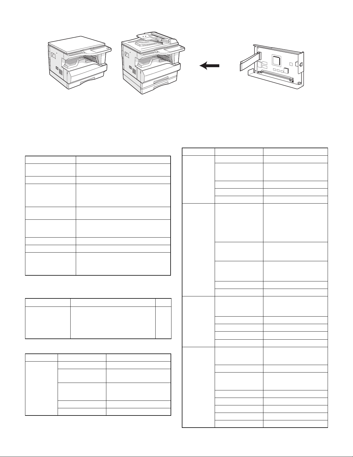
[1] SYSTEM CONFIGURATION
[2] SPECIFICATIONS
1. “Sharp Printer Language with
Compression (SPLC)” Printer mode
(AR-EB7)
A. Basic specification
Item Detail
Print Speed 10ppm (600dpi) (With the AR-EB7 installed)
Data resolution 300/600dpi
Input tray 4 Multi size tray
Option memory
Printer driver Two drivers for the case when the AR-EB7 is
Manual (Online manual)
Platform IBM PC/AT (Include compatible machine)
Support OS
(Printer Driver)
AR-160M (16ppm)/AR-200M (20ppm)
1 Multi Bypass tray
(Depending on conditions of the machine
and option installation.)
+16MB (With the AR-EB7 installed)
128/256/512M B can be added to the AR-EB7.
installed and when it is not are automatically
installed by plug & play.
Standard
Windows 95/98/Me
Windows NT4.0 Workstation (SP6 or later)
Windows 2000 Professional
Windows XP Home/Professional Edition
B. Printer driver specification
(1) System
Machine OS GDI
IBM PC/AT
(Include compatible
machine)
(2) Printing function specification
Main Copies 1-999
Windows 95/98/Me
Windows NT4.0 Workstation
(SP6 or later)
Windows 2000 Professional
Windows XP Home/Professional Edition
Function GDI Driver
Collate Collate
Uncollate
Document Style 1-sided
2-sided (Book)
2-sided (Tablet)
N-up printing 2/4
N-up Order Z
Yes
Function GDI Driver
Main
Paper Paper Size A3/B4/A4/B5/A5/B6/A6/
Advanced Print Quality Normal
Water-marks Watermark (None)/TOP SECRET/
N-up Border Yes/No
Duplex 1-sided
Binding Edge Yes/No
Booklet Possible
Booklet Binding Edge Yes/No
Custom Paper Size 1 size
Paper Selection • Auto Select
Fit to Page Yes/No
Image Orientation Portrait/Landscape
Image Adjustment Yes/No
Brightness 0 to 100
Contrast
2 Gradation print Yes/No
User setting Add/Update/Delete
Position Center
Size 6 to 300
Angle m90
Gray Scale 0 to 255
Edit Font Yes
On first page only Yes/No
2-sided (Book)
2-sided (Tablet)
Ledger(11x17)/Legal
(8.5 x 14)/Foolscap (8.5 x 13)/
Letter (8.5 x 11)/Invoice
(5.5 x 8.5)/Folio/Executive/
COM-10/DL/C5/8K/16K/
Custom
100 - 297mm(W)
148 - 431.8mm(H)
• Bypass
• Tray 1/2
Draft
Photo (without Win9x, Me)
0 to 100
CONFIDENTIAL/DRAFT/
ORIGINAL/COPY
X: m50
Y: m50
AR-EB7 SYSTEM CONFIGURATION
– 1 –
Page 5
(3) Scanner function specification
Type Flat bed color scanner
Scan system Document table/document feed unit
Light source White CCFL
Resolution Basic 600 x 1200dpi
Set range: 50 ~ 9600dpi
Document Sheet/Book
Effective scan range OC/SPF: Approx.297(V) x 431(H)
Scan speed OC/SPF: 2.8mm sec/line (Color)
Input data 1bit or 12bit
Output data 1bit or 8bit
Scan color Black and white binaryGray scaleFull color
Protocol TWAIN/WIA (XP only)/STI
Interface USB1.1
USB2.0 (It can be used according to conditions.)
(Option support: High speed mode)
(Supported when E-sort is installed)
Scanner utility Sharp Desk/Button Manager
Drop-out color Provided
Scanner button Provided (6)
Duplex scan Provided
Supported OS Windows98/ME/2000/XP
Void area Lead edge/rear edge (2.5mm) on the driver side
Left/right: 3.0mm
WHQL support Yes
Memory storage
JPEG-compression by hardware.
method
(4) System requrement
Computer IBM PC/AT (Include compatible machine)
Operating system Windows 95/98/Me
Windows NT 4.0 Workstation (SP5 or later)
Windows 2000 Professional
Windows XP Home/Professional Edition
Note: Hardware requirements such as CPU and RAM for your operat-
ing system must be satisfied.
(5) Print quality
Resolution 600dpi Print quality is selected from
2 Gradation print On 2-Gradation print function is ON.
*
Off
*Default
*
/Draft/Photo.
Normal
2-Gradation print function is OFF.
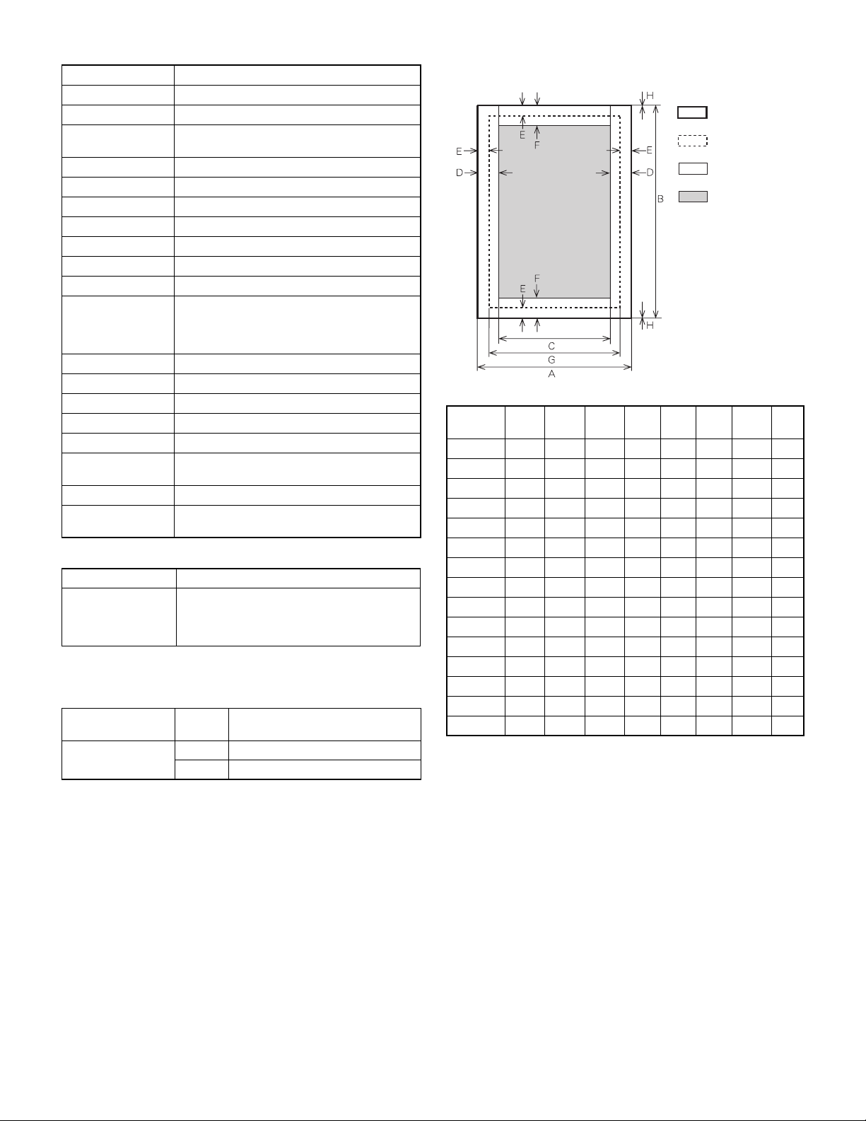
(6) Print area
Actual page size
Print area
Logic paper size
HP/GL
picture frame
Paper
Size
A3 7014 9920 6730 142 100 300 6814 0
B4 6070 8597 5786 142 100 300 5870 0
A4 4960 7014 4676 142 100 300 4760 0
B5 4298 6070 5770 142 100 300 4098 0
A5 3508 4960 3224 142 100 300 3308 0
Ledger 6600 10200 6300 150 100 300 6400 0
Legal 5100 8400 4800 150 100 300 4900 0
Letter 5100 6600 4800 150 100 300 4900 0
Invoice 3300 5100 3000 150 100 300 3100 0
Foolscap 5100 7800 4800 150 100 300 4900 0
Folio 4980 7800 4680 150 100 300 4780 0
Executive 4350 6300 4050 150 100 300 4150 0
COM-10 2474 5700 2174 150 100 300 2274 0
C5 3826 5408 3542 142 100 300 3626 0
DL 2598 5196 2314 142 100 300 2398 0
ABCDEFGH
AR-EB7 SPECIFICATIONS
– 2 –
Page 6
Actual page
size
Print area
Logic paper
size
HP/GL
picture
frame
Paper
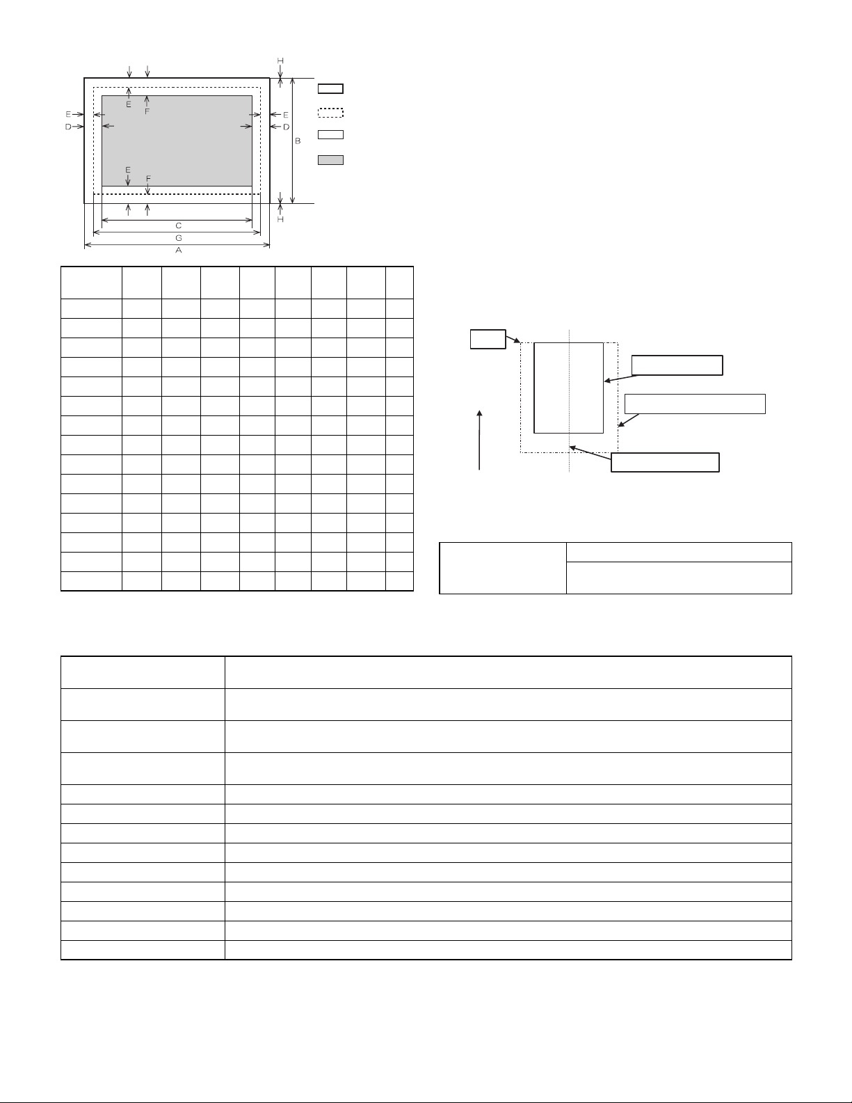
Size
A3 9920 7014 9684 118 100 300 9720 0
B4 8597 6070 8361 118 100 300 8397 0
A4 7014 4960 6778 118 100 300 6814 0
B5 6070 4298 5830 118 100 300 5870 0
A5 4960 3508 4720 118 100 300 4760 0
Ledger 8400 5100 8160 120 100 300 8200 0
Legal 8400 5100 8160 120 100 300 8200 0
Letter 6600 5100 6360 120 100 300 6400 0
Invoice 5100 3300 2860 120 100 300 4900 0
Foolscap 7800 5100 7560 120 100 300 7600 0
Folio 7800 4980 7560 120 100 300 7600 0
Executive 6300 4350 6060 120 100 300 6100 0
COM-10 5700 2474 3460 120 100 300 5500 0
C5 5408 3826 5172 118 100 300 5208 0
DL 5196 2598 4960 118 100 300 4996 0
ABCDEFGH
*Top margin
The set value is received from the digital copier, and data are m ade
according to the set value.
*Left margin
Since the paper size sensor is not set, the digital copier cannot recognize the size and direction of paper which is actually inserted.
Therefore, the left margin is set according to the paper size specified
in the print data sent from the computer, and print process is performed.
If the computer does not specify the paper size, or in the case of the
custom size, the left margin is set according to the default paper size.
(7) Print reference
This machine employs the center reference system.
Since the digital copier is not provided with the tray size detection feature, formatting and center distribution are performed not by the actual
paper size but by the paper size specified by the computer.
Origin
Actual paper size
Size specified by the HOST
Paper feed direction
Center reference line
D. Interface
Interface USB 1.1 (Standard)
USB 2.0 High speed
(With the AR-EB7 installed))
2. IMC2 board functions
*Sort function (Electronic sort) 100 sheets (max. 765 sheets) <copy mode> with A4 standard documents at 600dpi. Offset paper exit by the shifter
*Group function 100 sheets (max. 765 sheets) <copy mode> with A4 standard documents at 600dpi. Offset paper exit by the shifter
Rotation copy If there is paper of the same size as the document, the image is rotated to copy even though the paper i s set in the
2 in 1, 4 in 1 Copies of 2 pages or 4 pages are integrated into one surface. Divided by solid lines, (Selectable by the user pro-
Edge erase Images surrounding the document are erased when copying. (Adjustable in 5 ~ 20mm by the user program.)
Center erase The image at the center is erased when copying. (Adjustable in 5 ~ 20mm by the user program.)
Margin shift Binding margin is made at the left edge of the set documents. (Adjustable in 5 ~ 20mm by the user program.)
Memory for electronic sort 16MB
*Memory read capacity 600dpi: 100 sheets (Max. 765 sheets) <copy mode> of A4 standard documents (Sharp A4 standard document)
Memory expansion DIMM memory slot x 1, max. 256MB x 1 slot + 16MB (Max. 272MB in total)
USB2.0 Standard provision of E-sort (It can be used according to condition s .)
SPLC (JBIG-GDI) Supported when E-sort is installed.
ROPM Supported when E-sort is installed.
Caution: The number of sheets for the columns marked with “*” is calculated supposing that the same quantity is assigned to the ROPM memory and
the copy expansion memory.
function
function
different direction from the document direction.
gram.)
AR-EB7 SPECIFICATIONS
– 3 –
Page 7
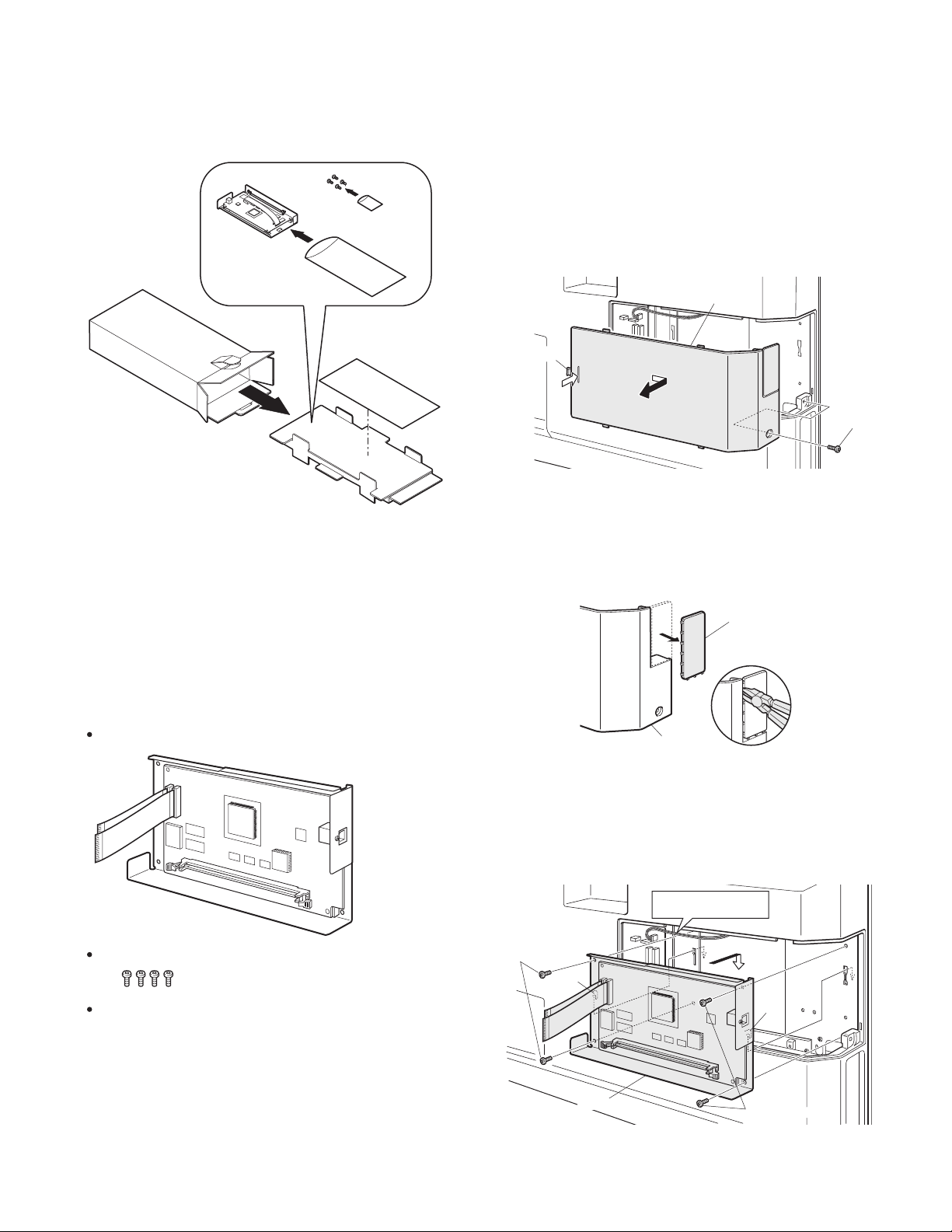
[3] UNPACKING AND INSTALLATION
w
1. Unpacking
<Before installation>
For improvement of workability, any part of the description in this
manual may be modified without prior notice. In this case, refer to
the service manual.
3. Installation procedure
Turn the main switch of the copier to the "OFF" position and then
remove the power plug of the copier from the power supply outlet.
1) Remove the rear cover.
Remove the screw, push the portion indicated by the arrow to
unlock the rear cover, and slide the cover to the right to remove it.
Rear cover
Pawl for
locking
Scre
2) Cut out the cut-out portion of the rear cover.
Cut out the cut-out portion with nippers or the like.
At this time, be careful about the orientation of the nippers so that
the cut plane of the rear cover is flat.
Cut-out portion
2. Parts included
IMC2 PWB (with frame)
screw (golden) M3 x 6: 4pcs.
Installation manual: 1 volume
Rear cover
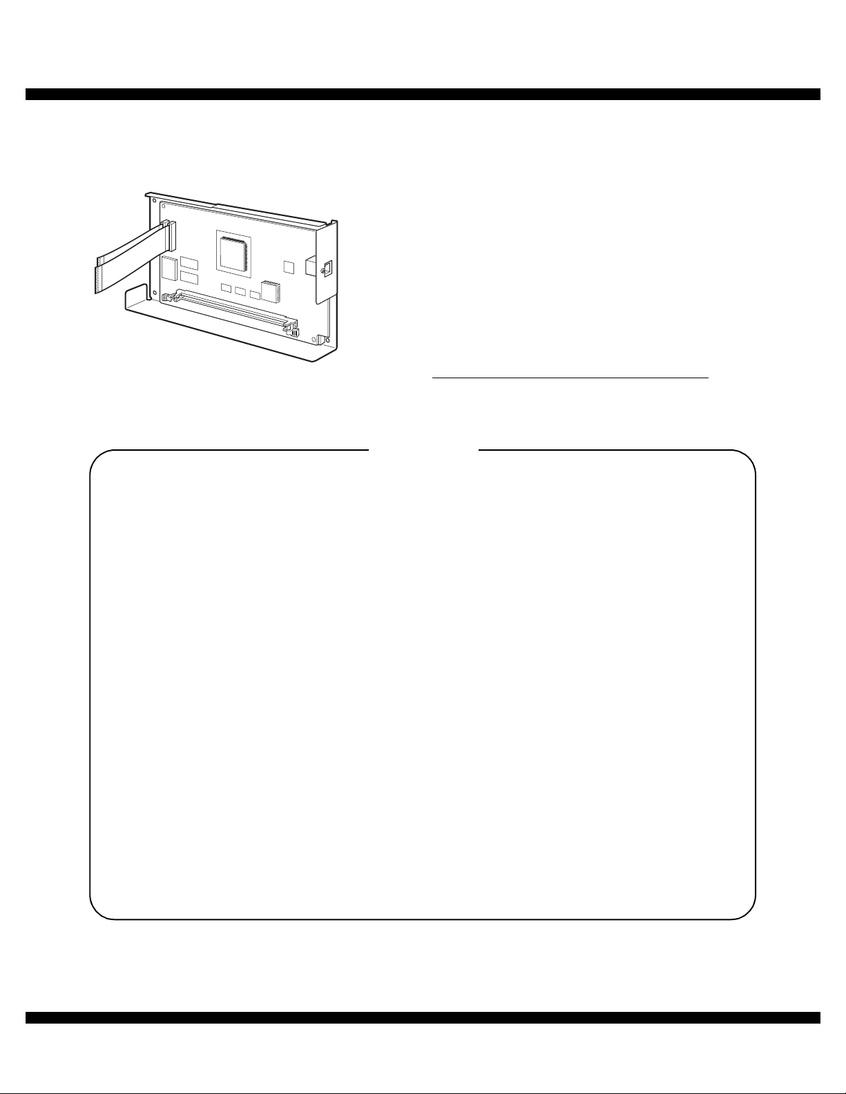
3) Attach the IMC2 PWB.
Fit the two pawls on the rear surface of the IMC2 PWB frame to the
mounting portions of the copier and secure the PWB with the four
supplied golden screws M3 x 6.
Take care not to get
the cable caught.
Screws (golden)
M3 x 6
Pawl
Pawl
IMC2 PWB
Screws (golden)
M3 x 6
AR-EB7 UNPACKIN G AND INSTALLATI ON
– 4 –
Page 8
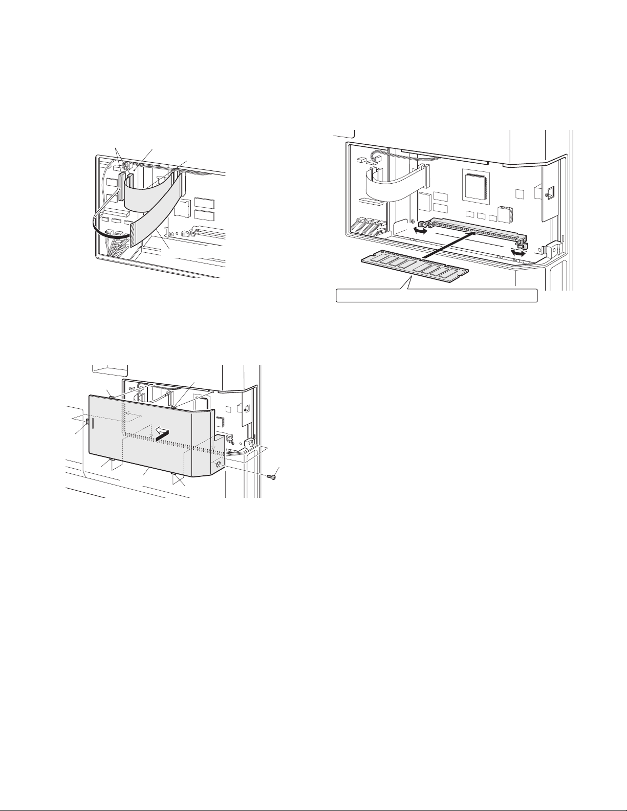
4) Connect the IMC2 PWB to the MCU PWB of the copier.
Connect the flat cables of the IMC2 PWB to the connectors of the
MCU PWB of the copier so that the shorter cable comes inside and
the longer cable comes outside as shown in the illustration.
Be careful about the orientation of the flat cable insertion and check
that both ends of each cable are securely inserted into the connector. (The terminal surface of each flat cable must have c ontact with
the connector terminals.)
4. Installation of additional memory
(After installation, proceed to step 5.)
1 Open the two locking clips of the socket.
2 Insert the memory matching the orientation of its notches.
3 Close the locking clips of the socket.
Connector
5) Attach the rear cover.
Fit the four pawls of the rear cover to the rear cabinet, slide the
cover to the left until it is locked, and then secure the cover with the
screw.
Pawl
Pawl for
locking
Pawl
Copier MCU PWB
Rear cabinet
Rear cover
Flat cable (shorter)
IMC2 PWB
Flat cable (longer)
Pawl
Pawl
Screw
1
3
3
2
As additional memory, use AR-SM5 (sold separately).
1
Insert the power plug of the copier into the power supply outlet
and turn on the power switch. Then, carry out the following procedure.
6) Check the IMC2 PWB.
Press the SORT/GROUP key on the operation panel to check that
the SORT mode indicator lights up.
7) Check printing.
For installation of the driver software on the computer, see the oper-
ation manual supplied with the copier.
Connect the USB cable, carry out printing from the computer, and
check that printing can be performed normally.
AR-EB7 UNPACKIN G AND INSTALLATI ON
– 5 –
Page 9
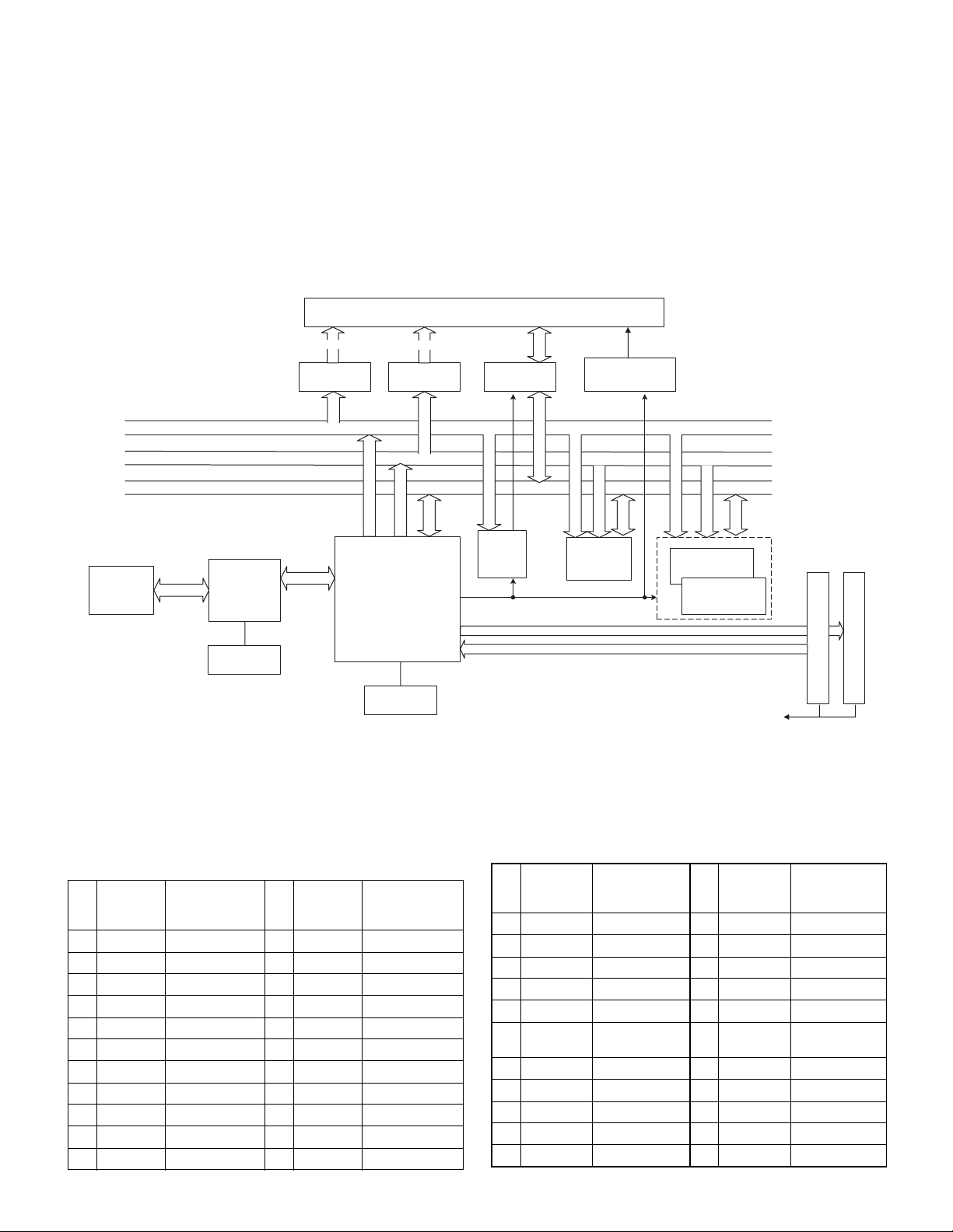
[4] ELECTRICAL SECTION
The OA982 board mounted on the IMC2 board inputs and outputs image data to and from the MCU board, controls SDRAM memory, and communicates with USB2.0 devices.
SDRAM memory is used to store programs and image data as well as for a working area.
USB 2.0 devices communicate with a PC through a USB2.0 cable at a rate of 480 Mbps.
SDRAM memory can be expanded by using 1BANK SDRAM DIMM (AR-SM5).
Communications between the OA982 and the AR-SM5 is held using an ASIC-controlled BUFFER IC (74VCX16244/16245).
1. Block diagram
CN6 168PIN DIMM SOCKET
(For 1BANK SNR SDRAM DIMM)
CONTROL BUS ADDRESS BUS
IC28 BUFFER
74VCX16244
CONTROL SIGNAL (/CS,/RAS,/CAS,/WE etc.)
ADDRESS BUS
DATA BUS
IC29 BUFFER
74VCX16244
DATA BUS
IC26 BUFFER
74VCX16245
/OE,/DIR
SDRAM CLK
81.2376MHz
IC6
ZeroDelayBuffer
CY2305
IC35
BUFFER
ASIC
USB2.0
Connector
USB2.0
High/Full
Speed
IC8
USB2.0Driver
ISP1581
Y1 XTAL
12.0000MHz
Peripheral
BUS(DMA)
8bit ADBUS
IC1
OA982
X1 XTAL
20.3094MHz
2. Pin arrangement
The table below shows connector pin arrangement between the MCU to IMC2 PWB.
• IMC2 side
Interface-1 CN2 (22FE-BT-VK-N)
Pin
No.
Signal
name
Processing of
connection
Pattern = “direc t”
Pin
No.
Signal
name
Processing of
connection
Pattern = “direct”
1 DGND (MCU 3 IMC) 12 PI_DATA2 MCU 3 IMC
2ESCMD IMC 3 MCU 13 PI_DATA1 MCU 3 IMC
3 /ESCRDY MCU 3 IMC 14 PI_DATA0 MCU 3 IMC
4 PI_WR MCU 3 IMC 15 /HSYNC MCU 3 IMC
5 PI_ACK MCU 3 IMC 16 /ESPAGE IMC 3 MCU
6 PI_REQ IMC 3 MCU 17 /PRLINE MCU 3 IMC
7 PI_DATA7 MCU 3 IMC 18 /RESET MCU 3 IMC
8 PI_DATA6 MCU 3 IMC 19 3.3V (MCU 3 IMC)
9 PI_DATA5 MCU 3 IMC 20 3.3V (MCU 3 IMC)
10 PI_DATA4 MCU 3 IMC 21 DGND (MCU 3 IMC )
11 PI_DATA3 MCU 3 IMC 22 DGND (MCU 3 IMC )
Interface-2 CN3 (22FE-BT-VK-N)
Pin
No.
1 DGND (MCU 3 IMC) 12
2 ESSTS MCU 3 IMC 13
3 /ESSRDY IMC 3 MCU 14
4 (PO_CS) NOT USE 15 /READY MCU 3 IMC
5 PO_ACK IMC 3 MCU 16 /SCLINE MCU 3 IMC
6 PO_REQ MCU 3 IMC 17 /ESDET IMC (GND)
7
8
9
10
11
IC2
8Mbit
FlashROM
SDRAM CLK 81.2376MHz
Signal
name
PO_DATA7
PO_DATA6
PO_DATA5
PO_DATA4
PO_DATA3
Pattern = “direct”
IMC 3 MCU 18 5V (MCU 3 IMC)
IMC 3 MCU 19 3.3V (MCU 3 IMC)
IMC 3 MCU 20 3.3V (MCU 3 IMC)
IMC 3 MCU 21 DGND (MCU 3 IMC)
IMC 3 MCU 22 DGND (MCU 3 IMC)
256Mbit SDRAM
256Mbit SDRAM
Pixel Output BUS (8bit DMA)
Pixel Input BUS (8bit DMA)
Processing of
connection
IC3
IC4
Pin
No.
3.3V
Signal
name
PO_DATA2
PO_DATA1
PO_DATA0
CN2 22pinFFC (To MCU)
CN3 22pinFFC (To MCU)
Processing of
connection
Pattern = “direct”
IMC 3 MCU
IMC 3 MCU
IMC 3 MCU
3 MCU
AR-EB7 ELECTRICAL SECTION
– 6 –
Page 10

[5] USER PROGRAMS
1. List
With the AR-EB7, the following user settings can be made:
[6] 1in1/4in1 solid- and broken-line frame setting
[7] Rotation copy function setting
[16] Adjustment of frame deletion/center deletion width
[17] Change in 2in1 combination
[18] Change in 4in1 combination
[21] Selection of binding margin position
[22] Adjustment of binding margin
[24] Allocation of memory capacity to printer
[33] Selection of USB2.0 mode
[6] FLASH ROM VERSION UP
2. Initialization
(Procedures for setting the serial number)
Set the serial number on the side of the PC for download. It is not necessary to set the serial number again at a later time, even if software is
restarted.
1) PC side:
Start the "Maintenance.exe" and select the model icon of main
body.
(Connection with the main body is not necessary for setting the
serial number only. However, for the set serial number to be
reflected into the main body, a connection should be made between
the PC and the main body in download mode for download.)
PROCEDURE
1. Preparation
Write the download data (the file with the extension dwl) to the main
body.
Necessary files for download
• Maintenance.exe (Maintenance software)
• ProcPegasus.mdl
• ProcPegasus.ini
• ProcPegasus.fmt
• Pegasus.inf
• Usbscan.sys
• Download file:***.dwl
Note:
• The Download file(***.dwl ) and the like that are to be downloaded
should be copied, in advance, into folders that have a maintenance
program.
• When creating a folder for a maintenance tool in the PC, be sure
that no lengthy folder name is included in the path.
(Example)
Incorrect c:\Pegasus Download Tool
Correct c:\Pegasus\Downtool
2) Select the "Option" in the menu bar and click on the "Serial Number
Setting".
3) Make the setting of the serial number following the instructions below.
Place of production code (P): Code number assigned on the basis of a
Enter the number three "3" for service.
ID cord (I): Code number assigned by PC. (0 - 99)
If there is more than one computer that uses "MaintenanceTool.exe",
then assign a different code number to each PC.
When the setting is completed, push down the button "OK".
4) The procedures for the change of the serial number has been completed.
AR-EB7 USER PROG R AM S
– 7 –
production place. (0 - 99)
Page 11

3. Download procedure
1) Main body side:
Executable by performing the Service Simulation No. 49-01 (Flash
Rom program-writing mode).
(A word "d" app ear s o n t he LC D t o d eno te th e do wn loa d mode status.)
2) Connect the PC and the main body with the download cable (USB
cable).
(Be sure to use a USB cable for connection. USB2.0 of the AR-EB7
is not applicable.)
3) PC side:
Boot the maintenance program. Select the model icon of main
body.
6) PC side:
Confirm a tree is displayed under the "Special (MCU/IMC2/FAX)"
on the maintenance program". (If no tree is displayed, confirm that
the USB is connected and select the "Reconnect" (the above 5)
again.)
7) PC side:
Double click "Special (MCU/MCU2/FAX)" in the main tree item to
develop the sub tree items, and double click "DWL Download" in
the sub tree items.
4) PC side:
Confirm that the "Simulation Command List" tree is displayed on the
maintenance program.
5) PC side:
When the message "the main body has not got started running" is
displayed on the lowest area of the figure below after the "maintenance program" is started up, select the "File" and then "Reconnect" in the menu bar.
8) PC side:
Specify the download file (*.dwl).
9) PC side:
The download file is specified, download is automatically performed.
The "Automatic paper selection" lamp and "Start" lamp will blink
approximately 15 seconds after the download file is specified.
AR-EB7 FLASH ROM VERSION UP PROCEDURE
– 8 –
Page 12

10) PC side:
When the message below is displayed, download is completed.
Completion message: DOWNLOAD COMPLETED
Note (Important):
• Be sure that the power is not turned off and the USB c able is not
removed until the word "OFF" appears.
11) Main body side:
Wait until the word "OFF" appears on the operation panel. The
appearance of "OFF" indicates the completion of the download
(writing into ROM).
Turn the power off.
12) After-process: Terminate the maintenance program, and turn on the
power of the main body.
After the download (data transmission) has been completed, exit the
software program. The USB cable can be removed at this point.
Note:
• For making a second connection with another machine, select the
"File" and "Reconnect" in the menu bar on the maintenance program at the time of the USB being re-connected. Repeat the previous procedures from the above 5).
4. Installation procedure
A. USB joint maintenance program installation
The driver is installed by plug and play.
B. Installation procedure on Windows XP
1) Main body side:
Executable by performing the Service Simulation No. 49-01 (Flash
Rom program-writing mode).
(A word "d" appea r s on the LC D t o d en ote th e d ow nlo ad m od e st atu s.)
2) Connect the machine and the PC with a USB cable.
(Be sure to use a USB cable for connection. USB2.0 of the AR-EB7
is not applicable.)
3) Check that the following display is shown.
Select "Install from a list or the specific location" and press the
NEXT button.
4) Select "Include this location in the serch". If the retrieval area does
not include the folder which includes the maintenance tool driver
(Pegasus.inf), select "Browse".
If the folder path is properly shown, press the NEXT button to go to
procedure 7).
*Forbidden actions while downloading (Important )
Failure in the download concerned may not allow you to conduct the
subsequent download procedures. Added care should be taken to avoid
having the situation below arise while downloading.
• Switching off the main body.
• Disconnecting the download cable (USB cable).
AR-EB7 FLASH ROM VERSION UP PROCEDURE
– 9 –
Page 13

5) Select the folder which includes the maintenance tool driver
(Pegasus.inf), and press the OK button.
(When the driver is included in the "C:\Pegasus" folder:)
8) When installation is completed, the following display is shown.
Press the Finish button.
6) Check that the path to the folder which includes the maintenance
tool driver (Pegasus.inf) is shown, and press the NEXT button.
7) Check that the following display is shown. Press the Continue Anyway button.
The installation procedure (on Windows XP) is completed with the
above operation.
C. Installation procedure on Windows 2000
1) Main body side:
Executable by performing the Service Simulation No. 49-01 (Flash
Rom program-writing mode).
(A word "d" appea r s on the LC D t o d en ote th e d ow nlo ad m od e st atu s.)
2) Connect the machine and the PC with a USB cable.
(Be sure to use a USB cable for connection. USB2.0 of the AR-EB7
is not applicable.)
3) Check that the new hardware search wizard is shown. Press the
NEXT button.
AR-EB7 FLASH ROM VERSION UP PROCEDURE
– 10 –
Page 14

4) Select "Serch for a suitable driver for my device" and press the
NEXT button.
5) Select "Specify a location" and press the NEXT button.
7) Specify the folder which includes the maintenance tool driver
(Pegasus.inf), and press the OPEN button.
Check that the path to the folder which includes the maintenance
tool driver (Pegasus.inf) is properly displayed, and press the OK
button.
(When the maintenance tool driver is included in the folder of
"D:\Pegasus")
8) Press the NEXT button, and installation is started.
6) Press the "Browse" button. Specify the folder which includes the
maintenance tool driver (Pegasus.inf)
9) When installation is completed, the following display is shown.
Press the Finish button.
The installation procedure of the joint maintenance program on Windows 2000 is completed with the above operation.
AR-EB7 FLASH ROM VERSION UP PROCEDURE
– 11 –
Page 15

B
B
B
C10
NM
_SDRAM_CKE
3943
VDDQ
VDDQ
VDDQ
CLK
CKE
37
_SDRAM_CLK
_SDRAM_CKE
_SDRAM_CLK
3.3V
11427
VDD
VDD
VDD
DQM
391938
_SDRAM_DQMA0
B
C21
10U/16V
+
C25
0.1U
K4S560832D
_SDRAM_DATA[15:0]
_SDRAM_DATA9
_SDRAM_DATA11
_SDRAM_DATA8
_SDRAM_DATA10
245781011
DQ0NCDQ1NCDQ2NCDQ3
A0A1A2A3A4A5A6A7A8A9A10
IC4
2324252629303132333422
SDRAM_ADDR0
SDRAM_ADDR2
SDRAM_ADDR3
SDRAM_ADDR1
SDRAM_ADDR4 _SDRAM_DATA12
SDRAM_ADDR[12:0]
_SDRAM_DATA15
_SDRAM_DATA14SDRAM_ADDR6
_SDRAM_DATA13
DQ4NCDQ5NCDQ6NCDQ7
SDRAM_ADDR7
SDRAM_ADDR8
SDRAM_ADDR5
A12
A11
35
36
SDRAM_ADDR12
SDRAM_ADDR9
SDRAM_ADDR11
SDRAM_ADDR10
SDRAM_BANK[1:0]
BA0
BA1
20
21
_SDRAM_CS0_L
SDRAM_BANK1
SDRAM_BANK0
C24
0.1U
C23
0.1U
C22
0.1U
54
41
28
61246
52
VSS
VSS
VSS
VSSQ
VSSQ
VSSQ
VSSQ
NC
NC
NC
NC
13
424445474850515315
40
D
D
D
D
C1
1/4
12345678
12345678
12345678
12345678
_SDRAM_DATA[15:0]
_SDRAM_DATA0
_SDRAM_DATA1
293133353840424430323436394143
IO0
IO1
IC2
A0A1A2A3A4A5A6A7A8A9A10
25242322212019
SDRAM_ADDR2
SDRAM_ADDR1
SDRAM_ADDR[12:0]
_SDRAM_DATA[15:0]
_SDRAM_DATA3
_SDRAM_DATA5
_SDRAM_DATA6
_SDRAM_DATA4
_SDRAM_DATA2
IO2
IO3
IO4
IO5
SDRAM_ADDR7
SDRAM_ADDR6
SDRAM_ADDR5
SDRAM_ADDR4
SDRAM_ADDR3
_SDRAM_DATA7
IO6
IO7
IO8
IO9
8765432
18
SDRAM_ADDR10
SDRAM_ADDR9
SDRAM_ADDR8
SDRAM_ADDR11
_SDRAM_DQMA0
_SDRAM_DQMB0
3.3V
IO10
IO11
IO12
A11
A12
SDRAM_BANK0
SDRAM_ADDR12
SDRAM_BANK1
SDRAM_BANK[1:0]
_SDRAM_DQMB1
_SDRAM_DQMA1
R4
0J
SDRAM_ADDR[12:0]
TP894 TP
SDRAM_ADDR0
45
IO13
IO14
IO15/A-1
A13
A14
A15
A16
A17
A18NCWE
1
481716131112472628
_SDRAM_DATA8
_SDRAM_DQMB1
_SDRAM_DQMB0
SDRAM_RAS_L
SDRAM_CAS_L
SDRAM_WE_L
3.3V
_SDRAM_DATA[15:0]
_SDRAM_CS1A_L
_SDRAM_CS1B_L
_SDRAM_CS0_L
3.3V
A19
A20
_SDRAM_DATA9
_SDRAM_DQMA1
_SDRAM_DQMA0
R417
NM
VCC
CEOERY/BY
ROM_CS_L
10KJ
RY_BY
C2
0.1U
15910
3.3V
C
C
C
C
274637
GND
GND
RESET
BYTE
WP/ACC
14
MBM29LV160B-90PFTN or LH28F800BJE-PBTL90
TP893 TP
R5
4.7KJ
*change-1(2003.3.17)
RESET_L
_SDRAM_CLK
_SDRAM_CKE
_SDRAM_DATA2
_SDRAM_DATA1
_SDRAM_DATA4
_SDRAM_DATA3
_SDRAM_DATA0
245781011
DQ0NCDQ1NCDQ2NCDQ3
A0A1A2A3A4A5A6A7A8A9A10
IC3
2324252629303132333422
SDRAM_ADDR3
SDRAM_ADDR1
SDRAM_ADDR0
SDRAM_ADDR4
SDRAM_ADDR2
SDRAM_ADDR[12:0] _SDRAM_DATA[15:0]
_SDRAM_DATA7
_SDRAM_DATA5
_SDRAM_DATA6
DQ4NCDQ5NCDQ6NCDQ7
SDRAM_ADDR7
SDRAM_ADDR6
SDRAM_ADDR5
SDRAM_ADDR8
A12
A11
35
36
SDRAM_ADDR9
SDRAM_BANK0
SDRAM_ADDR10
SDRAM_ADDR11
SDRAM_ADDR12
SDRAM_BANK[1:0]
C9
BA0
BA1
20
21
SDRAM_BANK1
_SDRAM_CS0_L
NM
_SDRAM_CS0_L
3.3V
49
VDDQ
RAS
WE
CAS
CS
181617
SDRAM_RAS_L
SDRAM_CAS_L
SDRAM_WE_L
3.3V
49
VDDQ
RAS
WE
CAS
CS
181617
SDRAM_CAS_L
SDRAM_WE_L
SDRAM_RAS_L
3943
VDDQ
VDDQ
VDDQ
CLK
CKE
37
_SDRAM_CLK
_SDRAM_CKE
_SDRAM_CLK
A
3.3V
11427
VDD
VDD
VDD
DQM
391938
_SDRAM_DQMA1
C45
10U/16V
+
C49
0.1U
C48
0.1U
C47
0.1U
C46
0.1U
54
41
28
61246
52
VSS
VSS
VSS
VSSQ
VSSQ
VSSQ
VSSQ
NC
NC
NC
13
424445474850515315
40
21
21
21
21
K4S560832D
NC
3
3
3
3
TP885 TP
_SDRAM_DATA0
_SDRAM_DATA2
_SDRAM_DATA3
_SDRAM_DATA1
678
123
BR1 10JX4
TP4 SDRAM_DATA1
TP8 SDRAM_DATA3
TP6 SDRAM_DATA2
TP2 SDRAM_DATA0
SDRAM_DATA3
SDRAM_DATA0
SDRAM_DATA1
SDRAM_DATA2
74
SDRAM_DATA2
SDRAM_DATA1
SDRAM_DATA0
IC1
PI_LINE_SYNC/GP_D6
PI_TR_TGEN
PI_TGEN6
119
120
124
TP7 PI_WR
TP5 PI_TGEN6
TP1 PI_LINE_SYNC
TP3 PI_TGEN7
1. IMC2 PWB
[7] CIRCUIT DIAGRAM
TP886 TP
_SDRAM_DATA4
_SDRAM_DATA6
_SDRAM_DATA5
678
4 5
123
BR2 10JX4
TP12 SDRAM_DATA5
TP10 SDRAM_DATA4
TP14 SDRAM_DATA6
SDRAM_DATA5
SDRAM_DATA6
SDRAM_DATA4
SDRAM_DATA6
SDRAM_DATA5
SDRAM_DATA4
SDRAM_DATA3
PI_TGEN5
PI_TGEN4
PI_TGEN3
PI_TGEN2
125
126
127
128
TP11 PI_ACK
TP13 PI_REQ
TP9 PI_TGEN4
PI_WR
PI_ACK
PI_REQ
D
D
D
D
TP887 TP
_SDRAM_DATA8
_SDRAM_DATA11
_SDRAM_DATA10
_SDRAM_DATA9
_SDRAM_DATA7
678
123
4 5
4 5
BR3 10JX4
TP20 SDRAM_DATA9
TP22 SDRAM_DATA10
TP16 SDRAM_DATA7
TP24 SDRAM_DATA11
TP18 SDRAM_DATA8
SDRAM_DATA7
SDRAM_DATA11
SDRAM_DATA8
SDRAM_DATA9
SDRAM_DATA10
SDRAM_DATA9
SDRAM_DATA8
SDRAM_DATA7
SDRAM_DATA10
PI_TGEN1
PI_TGEN0
PI_DATA7
PI_DATA6
129
131
132
133
134
TP23 PI_DATA5
TP19 PI_DATA7
TP15 PI_TGEN1
TP21 PI_DATA6
TP17 PI_TGEN0
PI_DATA6
PI_DATA7
TP888 TP
_SDRAM_DATA12
_SDRAM_DATA13
_SDRAM_DATA14
_SDRAM_DATA15
678
123
4 5
BR4 10JX4
TP28 SDRAM_DATA13
TP26 SDRAM_DATA12
TP30 SDRAM_DATA14
TP32 SDRAM_DATA15
SDRAM_DATA15
SDRAM_DATA13
SDRAM_DATA14
SDRAM_DATA12
535556575860616263656667687273
SDRAM_DATA15
SDRAM_DATA14
SDRAM_DATA13
SDRAM_DATA12
SDRAM_DATA11
PI_DATA5
PI_DATA4
PI_DATA3
PI_DATA2
PI_DATA1
135
137
138
141
TP27 PI_DATA3
TP29 PI_DATA2
TP31 PI_DATA1
TP25 PI_DATA4
PI_DATA5
PI_DATA4
PI_DATA3
PI_DATA2
PI_DATA1
TP889 TP
_SDRAM_DQMA0
_SDRAM_DQMB1
_SDRAM_DQMA1
_SDRAM_DQMB0
678
123
4 5
BR5 10JX4
TP40 SDRAM_DQMB1
TP34 SDRAM_DQMA0
TP38 SDRAM_DQMA1
TP36 SDRAM_DQMB0
SDRAM_DQMB1
SDRAM_DQMB0
SDRAM_DQMA0
SDRAM_DQMA1
105
106
107
109
SDRAM_DQMB1
SDRAM_DQMA1
SDRAM_DQMB0
SDRAM_DQMA0
PP_HIDRIVE/USART1_RX
PP_DRIVE/USART1_TX
PP_NINIT
PI_DATA0
143
145
146
147
142
TP35 PP_HIDRIVE
TP33 PI_DATA0
TP37 PP_DRIVE
TP41 PP_NFAULT
TP39 PP_NINIT
RY_BY
PI_DATA0
USART1_ TX
USART1_RX
ROM_CS_L
TP891 TP
TP892 TP
TP890 TP
_SDRAM_CS0_L
_SDRAM_CS1A_L
_SDRAM_CS1B_L
ROM_CS_L
SDRAM_WE_L
R3 10J
R1 10J
R2 10J
TP49 ROM_CS_L
TP52 SDRAM_WE_L
TP43 SDRAM_CS0_L
TP47 SDRAM_CS1B_L
TP45 SDRAM_CS1A_L
SDRAM_CS0_L
SDRAM_CS1B_L
SDRAM_CS1A_L
SDRAM_WE_L
75
77
102
104
111
ROM_CS_L
SDRAM_WE_L
SDRAM_CS0_L
SDRAM_CS1A_L
SDRAM_CS1B_L
PP_NFAULT
PP_NSELECTIN
PP_NAUTOFD
PP_SELECT
PP_PERROR
PP_BUSY
PP_NACK
151
152
153
154
155
156
TP51 PP_NACK
TP46 PP_SELECT
TP42 PP_NSELECTIN
TP50 PP_BUSY
TP44 PP_NAUTOFD
TP48 PP_PERROR
USB_FUNC
CN11
123
3.3V
UART-1 (TP or Connector)
SDRAM_ADDR[12:0]
SDRAM_CAS_L
SDRAM_RAS_L
TP54 SDRAM_CAS_L
TP56 SDRAM_RAS_L
TP61 SDRAM_ADDR1
TP59 SDRAM_ADDR0
SDRAM_ADDR0
SDRAM_RAS_L
SDRAM_CAS_L
SDRAM_ADDR1
101
110
SDRAM_RAS_L
SDRAM_CAS_L
SDRAM_ADDR0
PP_DATA7
PP_DATA6
PP_DATA5
PP_DATA4
157
159
160
161
162
TP57 PP_DATA5
TP58 PP_DATA4
TP53 PP_DATA7
TP55 PP_DATA6
TP60 PP_DATA3
4
USART1_RX
USART1_TX
TP69 SDRAM_ADDR5
TP65 SDRAM_ADDR3
TP67 SDRAM_ADDR4
TP63 SDRAM_ADDR2
TP70 SDRAM_ADDR6
SDRAM_ADDR3
SDRAM_ADDR6
SDRAM_ADDR2
SDRAM_ADDR5
SDRAM_ADDR4
SDRAM_ADDR6
SDRAM_ADDR5
SDRAM_ADDR4
SDRAM_ADDR3
SDRAM_ADDR2
SDRAM_ADDR1
PP_DATA3
PP_DATA2
PP_DATA1/USART1_CK
PP_DATA0
PP_NSTROBE
163
165
166
167
TP66 PP_DATA0
TP64 PP_DATA1
TP62 PP_DATA2
TP68 PP_NSTROBE
B4B-PH-K-S(NM)
TP883
CLK
TP81 SDRAM_ADDR12
TP76 SDRAM_ADDR9
TP74 SDRAM_ADDR8
TP72 SDRAM_ADDR7
TP77 SDRAM_ADDR10
TP79 SDRAM_ADDR11
SDRAM_ADDR7
SDRAM_ADDR8
SDRAM_ADDR11
SDRAM_ADDR9
SDRAM_ADDR10
SDRAM_ADDR12
80
SDRAM_ADDR9
SDRAM_ADDR8
SDRAM_ADDR7
SDRAM_ADDR11
SDRAM_ADDR10
SDRAM_ADDR12
REG_A9/PB_NCS1
REG_A8/PB_NCS2
BASE_CLK/GP_PWM1
MAIN_CLK/GP_PWM0
CLK_EXT/GP_PWM2
178
180
168
170
169
TP71 BASE_CLK
TP80 PB_NCS2
TP73 CLK_EXT
TP75 MAIN_CLK
TP78 PB_NCS1
BASE_CLK
CLK_EXT
PB_DATA[7:0]
_SDRAM_CLK
_SDRAM_CKE
TP884
CKE
SDRAM_BANK[1:0]
R9 10J
R8 10J
TP89 SDRAM_CLK
TP86 SDRAM_BANK1
TP84 SDRAM_BANK0
TP91 SDRAM_CKE
SDRAM_CKE
SDRAM_BANK0
SDRAM_BANK1
SDRAM_CLK
78
7982838485899091929495969799100
SDRAM_CLK
SDRAM_CKE
SDRAM_BANK1
SDRAM_BANK0
REG_AD2/PB_DATA2
REG_AD3/PB_DATA3
REG_AD4/PB_DATA4
REG_AD5/PB_DATA5
REG_AD6/PB_DATA6
REG_AD7/PB_DATA7
187
186
185
183
182
181
TP83 PB_DATA6
TP85 PB_DATA5
TP82 PB_DATA7
TP90 PB_DATA2
TP87 PB_DATA4
TP88 PB_DATA3
PB_DATA7
PB_DATA4
PB_DATA5
PB_DATA6
PB_DATA2
PB_DATA3
C
C
C
C
R10 4.7KJ
3.3V
R11
+
TP881
VDD7
7
PLLCS_VDDA
REG_AD0/PB_DATA0
REG_AD1/PB_DATA1
REG_ADDR_VALID/PB_NCS0
REG_RD_L/PB_NCS3
REG_WR_L/PB_NAE0
REG_CS_L/PB_NAE1
REG_RDY/PB_NWE
189
188
190
194
195
196
197
TP97 PB_NAE1
TP95 PB_NCS3
TP92 PB_DATA1
TP93 PB_DATA0
TP96 PB_NAE0
TP94 PB_NCS0
TP98 PB_NWE
PB_DATA0
PB_DATA1
PB_NAE0
PB_NWE
PB_NCS3
1J
C3
47U/16V
TP882
VDD149
C5
1U
C4
0.01U
6
PLLCS_VSSA
GP_C0/PB_ADDR0
GP_C1/PB_ADDR1
GP_C2/PB_ADDR2
GP_C3/PB_ADDR3
INTERRUPT_L/PB_NOE
199
201
202
203
204
198
TP99 PB_NOE
TP101 PB_ADDR1
TP100 PB_ADDR0
TP103 PB_ADDR3
TP104 PB_ADDR4
TP102 PB_ADDR2
PB_ADDR3
PB_ADDR0
PB_ADDR2
PB_ADDR1
PB_ADDR4
PB_ADDR[7:0]
PB_NOE
R14
+
149
PLLSS_VDDA
GP_C4/PB_ADDR4
GP_C5/PB_ADDR5
GP_C6/PB_ADDR6
GP_C7/PB_ADDR7
128
205
207
208
TP107 PB_ADDR7
TP106 PB_ADDR6
TP108 USART0_TX
TP105 PB_ADDR5
PB_ADDR6
PB_ADDR7
PB_ADDR5
1J
C6
47U/16V
C8
1U
C7
0.01U
148
PLLSS_VSSA
GP_B0/USART0_TX
GP_B1/USART0_RX
GP_B2/USART0_CK
GP_B3/ANA_SD1
GP_B4/DT_ACKB
GP_B5/DT_REQB
9
11121314151619
TP113 DT_REQB
TP109 USART0_RX
TP112 DT_ACKB
TP110 USART0_CK
TP111 GP_B3
ESCMD
DT_ACKB
ESSTS
DT_REQB
3.3V
VDD_IO
GP_B6/DT_ACKA
GP_B7/DT_REQA
TP114 DT_ACKA
TP116 GP_D0
TP115 DT_REQA
25
VDD_IO
VDD_IO
VDD_IO
VDD_IO
GP_D0/ADC_A0
GP_D1/ADC_A1
GP_D2/ADC_A2
GP_D3/ADC_CLK
21
22
TP119 GP_D3
TP117 GP_D1
TP118 GP_D2
TP120 GP_D4
/ESPAGE
/ESCRDY
/ESSRDY
WAKEUP
USBVBUS
+
3.3V
115
103
VDD_IO
VDD_IO
VDD_IO
VDD_IO
VDD_IO
VDD_IO
GP_D4/ADC_DATA
GP_D5/ADC_NCS
GP_A1
GP_A2/DC_CHY1
GP_A0
26282930313224
23
TP123 GP_A1
TP121 GP_D5
TP124 GP_A2
TP122 GP_A0
/READY
SCL
SDA
SUSPEND
R401
3.9KJ
C11
10U/16V
C20
0.1U
C19
0.1U
C18
0.1U
C17
0.1U
C16
0.1U
C15
0.1U
C14
0.1U
C13
0.1U
C12
0.1U
144
130
VDD_IO
VDD_IO
VDD_IO
VDD_IO
GP_A3/DC_CHX1
GP_A4/DC_PWM1
GP_A5/DC_CHY0
GP_A6/DC_CHX0
34
TP126 GP_A4
TP128 GP_A6
TP129 GP_A7
TP125 GP_A3
TP127 GP_A5
/SCLINE
/PRLINE
INT_USBD
R402
C400
B
B
B
B
+
3.3V
VDD_IO
TP135
3.3V
12293888170713659184620033184201713158
VDD_IO
VDD_IO
VDD_CORE
VDD_CORE
VDD_CORE
VDD_CORE
VDD_CORE
GP_A7/DC_PWM0
PO_LINE_SYNC/ANA_SCLK
PO_PAGE_SYNC/ANA_NCS
PO_REQ/ANA_SD0
PO_ACK/PDATA0/PDS0
PO_DONE/PDATA2/PDS2
PO_WR/PDATA1/PDS1
PO_DATA7/LHEAT/PAS_M
PO_DATA6/LCTRL/CFIRE2
37383940424344454748495051
TP137 PO_DATA7
TP131 PO_PAGE_SYNC
TP132 PO_REQ
TP133 PO_ACK
TP130 /HSYNC
TP134 PO_DONE
TP136 PO_WR
TP138 PO_DATA6
PO_ACK
PO_DATA6
PO_DATA7
PO_REQ
/HSYNC
4.7KJ
NC
C26
10U/16V
C34
0.1U
C33
0.1U
C32
0.1U
C31
0.1U
C30
0.1U
C29
0.1U
C28
0.1U
C27
0.1U
TP147
27
10
192
174
140
VSS_IO
VSS_IO
VDD_CORE
VDD_CORE
VDD_CORE
USB_DM
PO_DATA5/AGATE/CFIRE1
PO_DATA4/ACLK/MFIRE2
PO_DATA3/PENABLE/MFIRE1
PO_DATA2/PLOAD
PO_DATA1/PCLK
PO_DATA0/PDATA3/PAS_C
52
175
USB_DM
TP145
TP140 PO_DATA4
TP141 PO_DATA3
TP139 PO_DATA5
TP142 PO_DATA2
TP144 /PCLPRD
TP143 PO_DATA1
PO_DATA0
PO_DATA4
PO_DATA3
PO_DATA1
PO_DATA5
PO_DATA2
3.3V
VDD_CORE
VSS_IO
VSS_IO
USB_DP
176
USB_DP
TP146
VSS_IO
VSS_IO
+
VSS_IO
1086998358617766454
VSS_IO
C35
C43
C42
C41
C40
C39
C38
C37
C36
123
VSS_IO
VSS_IO
RESET_L
112
TP148 RESET_L
RESET_L
10U/16V
0.1U
0.1U
0.1U
0.1U
0.1U
0.1U
0.1U
0.1U
136
113
TP149 TDO
VSS_IO
TDO
TDO
CLK_EXT_OUT
TP156
R19
4.7KJ
CLK_EXT
CLK_EXT
1
2
VSS_IO
TEST_MODE0
172
177
JTAGSCAN0
VSS_CORE
VSS_CORE
TEST_MODE1
TP155 TEST_MODE1
TP154 TEST_MODE0
R17 4.7KJ
R18 4.7KJ
JTAGSCAN1
121
87
VSS_CORE
VSS_CORE
VSS_CORE
TP955
TP
139
VSS_CORE
TP157
XIN
191
173
VSS_CORE
VSS_CORE
XIN
XOUT
5
4
X1
C44
XOUT
XIN
R20 0J
20.3094MHz
12P
A A
A A
A A
A
OA-982
X2
3.3V
C50
12P
GND
OUT
3
BASE_CLK
/CONT
VDD
4
TP880
SG8002JC (20or56MHz)
22000P(NM)
C53
0.1U(NM)
C52
12P(NM)
C51
XOUT
87654
87654
87654
87654
150
20641193
179
164
VSS_IO
VSS_IO
VSS_IO
VSS_IO
TRST_L
TCK
TMS
TDI
114
116
117
118
TP152 TDI
TP151 TMS
TP153 TRST_L
TP150 TCK
TDI
TMS
TCK
TRST_L
AR-EB7 CIRCUIT DIAGRAM
– 12 –
Page 16

+
C70
C80
C79
C78
C77
C76
C75
C74
C73
C72
C71
+
C69
168
VCC
VCC
CB6
CB7
137
TP232 NC
47U/16V
0.1U
0.1U
0.1U
0.1U
0.1U
0.1U
0.1U
0.1U
0.1U
0.1U
112233243546468788596
47U/16V
VSS
VSS
VSS
VSS
NCNCNCNCNCNCNC
24253144485051
TP237 NC
TP234 NC
TP233 NC
TP239 NC
TP236 NC
TP235 NC
TP238 NC
A
107
116
127
138
148
152
162
21
21
21
VSS
VSS
VSS
VSS
VSS
VSS
VSS
VSS
VSS
VSS
VSS
NCNCNC
NC
NC
NCNCNC
NCNCNC
616280
108
109
132
134
135
145
146
TP240 NC
TP242 NC
TP244 NC
TP245 NC
TP246 NC
TP247 NC
TP241 NC
TP249 NC
TP248 NC
TP243 NC
21
VSS
VSS
VSS
NC
147
164
DIMM168pinConnector MO-161
TP250 NC
TP251 NC
3
3
3
3
B
B
B
JTAGSCAN0
JTAGSCAN1
EPSONTEST
EPSONINP1
8
1012141618
USB_FUNC
20
B20B-PHDSS-B
19
C
C
C
C
A_SDRAM_ADDR[12:0]
A_SDRAM_BANK[1:0]
A_SDRAM_BANK1
A_SDRAM_BANK0
A_SDRAM_ADDR10
A_SDRAM_ADDR9
A_SDRAM_ADDR11
A_SDRAM_ADDR12
126
A10
A11
A12
BA1
BA0
CN6
DQ58
DQ59
DQ60
DQ61
DQ62
DQ63
154
155
156
158
159
160
161
A_SDRAM_DATA14
A_SDRAM_DATA15
A_SDRAM_DATA10
A_SDRAM_DATA9
A_SDRAM_DATA13
A_SDRAM_DATA11
A_SDRAM_DATA12
A_SDRAM_DATA[15:0]
A_SDRAM_ADDR3
A_SDRAM_ADDR2
A_SDRAM_ADDR8
A_SDRAM_ADDR6
A_SDRAM_ADDR7
A_SDRAM_ADDR5
A_SDRAM_ADDR4
A9
DQ51
DQ52
DQ53
DQ54
DQ55
DQ56
DQ57
142
144
149
150
151
153
A_SDRAM_DATA6
A_SDRAM_DATA8
A_SDRAM_DATA5
A_SDRAM_DATA4
A_SDRAM_DATA2
A_SDRAM_DATA3
A_SDRAM_DATA7
A_SDRAM_RAS_L
A_SDRAM_WE_L
A_SDRAM_RAS_L
A_SDRAM_WE_L
A_SDRAM_ADDR0
A_SDRAM_ADDR1
33
117341183511936120371213812339122
115271113011445129
A0A1A2A3A4A5A6A7A8
/WE
/RAS
DQ45
DQ46
DQ47
DQ48
DQ49
DQ50
101
103
104
139
140
141
A_SDRAM_DATA0
A_SDRAM_DATA1
A_SDRAM_DATA0
A_SDRAM_DATA2
A_SDRAM_DATA1
TP208 /CS3
TP209 /CS1
A_SDRAM_CAS_L
A_SDRAM_CS1B_L
A_SDRAM_CAS_L
A_SDRAM_CS1B_L
/CS2
/CS3
/CAS
DQ40
DQ41
DQ42
DQ43
DQ44
100
A_SDRAM_DATA6
A_SDRAM_DATA8
A_SDRAM_DATA3
A_SDRAM_DATA5
A_SDRAM_DATA4
A_SDRAM_DATA7
A_SDRAM_CS1A_L
A_SDRAM_DQMB1
A_SDRAM_CS1A_L
/CS0
/CS1
DQ36
DQ37
DQ38
DQ39
A_SDRAM_DATA12
A_SDRAM_DATA11
A_SDRAM_DATA10
A_SDRAM_DATA9
D
D
D
D
R419
10KJ
C59
C58
3.3V 3.3V
0.01U
0.01U
RESET_L
R48 0J
/RESET
TP193
TP957
TP
C60
R41 68J
R52
10KJ(NM)
PST597KNR(NM)
IC5
3.3V
3.3V
100P
R64
RESET_IC_OUT
45
VoutVcc
M/RSUBGND
C63
NM
NM
MACHINESET
ONLY
0.1U(NM)
1 2 3
C61
0.1U(NM)
246
CN1
1357911131517
2/4
12345678
12345678
12345678
12345678
3.3V
R26 10KJ
R25 10KJ
R24 10KJ
R23 NM
R22 10KJ
R21 10KJ
TDO
TCK
TRST_L
TMS
TDI
TP166
TP161
TP164
TP162
TP163
678
123
4 5
BR11 33JX4
TCK
TDI
TMS
TDO
TRST_L
3.3V
A_SDRAM_DQMB1
A_SDRAM_DQMB0
A_SDRAM_DQMA0
A_SDRAM_DQMA0
A_SDRAM_DQMB0
113
130
131
DQMB2
DQMB3
DQMB4
DQMB5
DQMB6
DQMB7
DQ30
DQ31
DQ32
DQ33
DQ34
DQ35
A_SDRAM_DATA15
A_SDRAM_DATA14
A_SDRAM_DATA13
A_SDRAM_DATA14
A_SDRAM_DATA15
A_SDRAM_DATA13
B
SDA
10KJ
R420
SCL
A_SDRAM_DQMA1
A_SDRAM_DQMA1
_SDRAM_CLK_3
_SDRAM_CLK_2
_SDRAM_CLK_1
28294647112
42
1257916363128838281167
CK1
CK2
CK3
DQMB0
DQMB1
DQ23
DQ24
DQ25
DQ26
DQ27
DQ28
DQ29
A_SDRAM_DATA7
A_SDRAM_DATA9
A_SDRAM_DATA6
A_SDRAM_DATA11
A_SDRAM_DATA8
A_SDRAM_DATA10
A_SDRAM_DATA12
R71 0J
_SDRAM_CKE
_SDRAM_CLK_0
_SDRAM_CKE
CK0
CKE1
CKE0
DQ17
DQ18
DQ19
DQ20
DQ21
DQ22
A_SDRAM_DATA3
A_SDRAM_DATA2
A_SDRAM_DATA5
A_SDRAM_DATA4
A_SDRAM_DATA0
A_SDRAM_DATA1
3.3V
TP212 NC
TP210 NC
TP211 NC
R78 10KJ(NM)
R76 10KJ(NM)
R74 10KJ(NM)
166
165
WP
SA2
SA1
SA0
SCL
SDA
DQ10
DQ11
DQ12
DQ13
DQ14
DQ15
DQ16
A_SDRAM_DATA1
A_SDRAM_DATA0
A_SDRAM_DATA4
A_SDRAM_DATA5
A_SDRAM_DATA2
A_SDRAM_DATA3
A_SDRAM_DATA6
0J
0J
0J
3.3V
6182640414959738490102
VCC
VCC
VCC
VCC
DQ3
DQ4
DQ5
DQ6
DQ7
DQ8
DQ9
10111314151617192055565758606566676970717274757677868788899192939495979899
A_SDRAM_DATA10
A_SDRAM_DATA13
A_SDRAM_DATA12
A_SDRAM_DATA8
A_SDRAM_DATA11
A_SDRAM_DATA7
A_SDRAM_DATA9
R85
R84
R83
VCC
VCC
VCC
VCC
VCC
VCC
VCC
DQ0
DQ1
DQ2
CB0
CB1
2345789
21
22
TP222 NC
TP219 NC
A_SDRAM_DATA15
A_SDRAM_DATA14
110
124
133
143
157
VCC
VCC
VCC
VCC
CB2
CB3
CB4
CB5
52
53
105
106
136
TP226 NC
TP229 NC
TP225 NC
TP230 NC
TP227 NC
DEBUG ONLY
PO_DATA2
/READY
PO_DATA0
PO_DATA1
3.3V3.3V
C57
0.1U
R409
10KJ
R407
C56
5V
TP160
NM
NM
C55
47U/16V
47U/16V
0.1U
10KJ
R408
10KJ
R410
10KJ
R414
10KJ
R412
10KJ
R411
10KJ
R413
10KJ
TP159 3.3V
5V
3.3V
R28
R27
3.3V
TP158 3.3V
C54
/SCLINE
R36 0J
R32 0J
R34 0J
R40 0J
R38 0J
/ESDET
PO_DATA1
PO_DATA0
PO_DATA2
/SCLINE
/READY
TP176
TP170
TP172
TP168
TP174
TP178
22
CN3
CN2
/ESPAGE
/RESET
/PRLINE C62
/HSYNC
PI_DATA0
PI_DATA1
PI_DATA2
TP167
TP173
TP175
TP177
TP169
TP165
TP171
R30 0J
R39 0J
R31 0J
R29 0J
R33 0J
R35 0J
R37 0J
PO_DATA3
PO_DATA4
R47 0J
R45 0J
R43 0J
PO_DATA3
PO_DATA4
PO_DATA5
TP180
TP182
TP184
10111213141516171819202122
PI_DATA3
PI_DATA4
PI_DATA5
TP183
TP179
TP181
R46 0J
R42 0J
R44 0J
PO_DATA5
PO_DATA7
PO_DATA6
R56 10J
R54 0J
R51 0J
PO_REQ
PO_DATA6
PO_DATA7
TP186
TP192
TP190
PI_REQ
PI_DATA6
PI_DATA7
TP191
TP189
TP185
R50 0J
R53 0J
R55 0J
PO_REQ
PO_ACK
R58 0J
(PO_CS)
PO_ACK
TP197
TP195
PI_WR
PI_ACK
TP196
TP194
R59 10J
R57 10J
ESSTS
/ESSRDY
R63 10J
R61 0J
S
ESST
/ESSRDY
TP199
TP201
ESCMD
/ESCRDY
TP200
TP198
R62 0J
R60 10J
123456789101112131415161718192021
123456789
C402
68P
C401
68P
22FE-BT-VK-N
From For DC2-BUS
Connector
22FE-BT-VK-N
C404
C403
68P
_SDRAM_CLK_2
_SDRAM_CLK_0
_SDRAM_CLK_3
R65 0J
R67 0J
R69 0J
C66
39PF
C65
2200P
TP897 TP
TP898 TP
TP899 TP
C64
CLK4
CLKOUT
REF
CLK2
123
TP896 TP
TP895 TP
R66 0J
_SDRAM_CLK
_SDRAM_CLK
_SDRAM_CLK_1
C405
68P
0.1U
678
VDD
CY2305
CLK1
GND CLK3
4 5
CLK1
TP207
R70 0J
_SDRAM_CLK_0
87654
87654
87654
87654
3.3V
IC6
68P
PI_DATA2
PI_DATA3
PI_DATA4
PI_DATA5
PI_DATA6
PI_DATA7
PI_REQ
PI_ACK
PI_WR
ESCMD
/ESCRDY
B
B
B
C
C
C
C
B
A A
A
A A
A A
/ESPAGE
PI_DATA1
PI_DATA0
/HSYNC
/PRLINE
/RESET
D
D
D
D
AR-EB7 CIRCUIT DIAGRAM
– 13 –
Page 17

B
B
B
B
A_SDRAM_BANK[1:0]
A_SDRAM_BANK0
4 5
3.3V3.3V
TP908 TP
235689111213141617192022
42
31
18
7
IC29
SDRAM_BANK0
A_SDRAM_ADDR[12:0]
SDRAM_BANK[1:0]
BD
A_SDRAM_CS1A_L
A_SDRAM_CS1B_L
A_SDRAM_CAS_L
A_SDRAM_RAS_L
A_SDRAM_WE_L
TP875
A_SDRAM_BANK1
BR403
0JX4
BR404
0JX4
1 8
2 7
3 6
1 8
2 7
3 6
4 5
TP909 TP
1Y1
1Y2
1Y3
1Y4
2Y1
2Y2
2Y3
2Y4
VCC
VCC
VCC
VCC
1A4
1A3
1A2
1A1
2A4
2A3
2A2
2A1
434446473738404132333536262729
SDRAM_BANK1
SDRAM_CAS_L
SDRAM_RAS_L
AD
TP868
SDRAM_WE_L
SDRAM_CAS_L
SDRAM_RAS_L
_SDRAM_CS1B_L
_SDRAM_CS1A_L
A_SDRAM_DQMB0
A_SDRAM_DQMB1
A_SDRAM_DQMA0
A_SDRAM_DQMA1
TP876
BR405
0JX4
1 8
2 7
3 6
4 5
TP910 TP
3Y1
3Y2
3Y3
3Y4
3A4
3A3
3A2
3A1
AD
_SDRAM_DQMA1
_SDRAM_DQMB0
_SDRAM_DQMA0
_SDRAM_DQMB1
BD
BD
BD
BD
TP879
TP877
TP878
C131
C130
23
4Y1
4Y2
4Y3
4Y4
4OE
3OE
2OE
4A4
4A3
4A2
4A1
1OE
1
30
242548
AD
AD
AD
OE
OE
TP869
TP874
TP870
TP871
TP872
TP873
A_SDRAM_DATA13
A_SDRAM_DATA14
A_SDRAM_DATA12
A_SDRAM_DATA10
A_SDRAM_DATA11
A_SDRAM_DATA9
BR38
0JX4
BR37
0JX4
2 7
3 6
4 5
1 8
2 7
3 6
TP
TP901
1B1
1B2
1B3
1B4
1B5
1B6
1B7
VCC
VCC
VCC
VCC
1A1
1A2
1A3
1A4
1A5
1A6
1A7
C
C
C
C
A_SDRAM_DATA8
A_SDRAM_DATA6
A_SDRAM_DATA5
A_SDRAM_DATA4
A_SDRAM_DATA7
BR36
0JX4
1 8
2 7
3 6
4 5
1 8
TP
TP902
12
13141617192022
2B1
2B2
2B3
1B8
2A1
2A2
2A3
1A8
37
36353332302927
A_SDRAM_DATA1
A_SDRAM_DATA2
A_SDRAM_DATA3
A_SDRAM_DATA0
BR42
0JX4
1 8
2 7
3 6
4 5
TP
TP903
23
2B4
2B5
2B6
2B7
2B8
2A4
2A5
2A6
2A7
2A8
26
1
1DIR
2DIR
244825
C125
C124
GND
GND
GND
GND
GND
GND
GND
GND
1OE
2OE
A_SDRAM_DATA[15:0]
0.1U
0.1U
45
39
34
28
21
15
10
4
74VCX16245
D
D
D
D
3/4
12345678
12345678
12345678
12345678
A_SDRAM_DATA14
A_SDRAM_DATA15
A_SDRAM_DATA13
BR39
10KJX4
1 8
2 7
3 6
3.3V
A_SDRAM_DATA11
A_SDRAM_DATA8
A_SDRAM_DATA12
A_SDRAM_DATA10
A_SDRAM_DATA9
BR43
10KJX4
1 8
2 7
3 6
4 5
4 5
A_SDRAM_DATA7
A_SDRAM_DATA4
A_SDRAM_DATA2
A_SDRAM_DATA5
A_SDRAM_DATA3
A_SDRAM_DATA6
BR40
BR41
10KJX4
1 8
2 7
1 8
2 7
3 6
4 5
A_SDRAM_DATA1
10KJX4
3 6
A_SDRAM_DATA0
4 5
A_SDRAM_DATA15
4 5
TP
TP900
23568911
42
31
18
7
47464443414038
IC26
0.1U
0.1U
GND
GND
GND
GND
GND
GND
GND
GND
45
39
34
28
21
15
10
4
74VCX16244
A
21
21
21
21
3
3
3
3
_SDRAM_CS1B_L_SDRAM_CLK
SDRAM_RAS_L
RESET_L
_SDRAM_DATA7
_SDRAM_DATA8
_SDRAM_DATA6
_SDRAM_DATA5
_SDRAM_DATA0
_SDRAM_DATA2
_SDRAM_DATA3
_SDRAM_DATA4
TP947
TP856
NA2_IN2
TP948
NA2_IN1
TP857
DIR
EPSONTEST
OE
TP953 USB_ALE
TP954 USB_CS
R418
USB_ALE
4.7KJ
USB_CS
PB_NCS3
PB_NAE0
TP865 BD
235689111213141617192022
42
31
18
7
IC28
TP860 AD
SDRAM_ADDR[12:0]
A_SDRAM_ADDR8
A_SDRAM_ADDR9
A_SDRAM_ADDR11
A_SDRAM_ADDR10
A_SDRAM_ADDR12
BR400
0JX4
1 8
2 7
3 6
4 5
R400 0J
TP867 BD
TP866 BD
TP904 TP
TP905 TP
1Y1
1Y2
1Y3
1Y4
2Y1
2Y2
2Y3
2Y4
VCC
VCC
VCC
VCC
1A4
1A3
1A2
1A1
2A4
2A3
2A2
2A1
434446473738404132333536262729
SDRAM_ADDR11
SDRAM_ADDR8
SDRAM_ADDR9
SDRAM_ADDR10
SDRAM_ADDR12
TP862 AD
TP861 AD
A_SDRAM_ADDR4
A_SDRAM_ADDR6
A_SDRAM_ADDR5
A_SDRAM_ADDR7
A_SDRAM_ADDR3
BR401
0JX4
1 8
2 7
3 6
4 5
4 5
TP906 TP
3Y1
3Y2
3Y3
3Y4
3A4
3A3
3A2
3A1
30
SDRAM_ADDR5
SDRAM_ADDR3
SDRAM_ADDR6
SDRAM_ADDR7
SDRAM_ADDR4
A_SDRAM_ADDR2
A_SDRAM_ADDR0
A_SDRAM_ADDR1
BR402
0JX4
1 8
2 7
3 6
TP907 TP
23
4Y1
4Y2
4Y3
4Y4
4A4
4A3
4A2
4A1
1OE
1
SDRAM_ADDR1
SDRAM_ADDR0
SDRAM_ADDR2
C129
0.1U
C128
0.1U
GND
45
GND
39
GND
34
GND
28
GND
21
GND
15
GND
10
GND
4
4OE
3OE
2OE
242548
74VCX16244
OE
OE
TP864
TP863
_SDRAM_DATA15
_SDRAM_DATA14
_SDRAM_DATA12
_SDRAM_DATA11
_SDRAM_DATA9
_SDRAM_DATA13
_SDRAM_DATA10
_SDRAM_DATA[15:0]
_SDRAM_CS1A_L
SDRAM_CAS_L
SDRAM_WE_L
EPSONINP1
VSS
INP0
CS1A_L
_SDRAM_CLK
NA1_OUT
TEST_OUT1
VSS
TP951 TEST_OUT1
VDD
NA1_IN1
TP949 NA1_IN1
TP950 NA1_IN2
VDD
INP1
NA1_IN2
VDD
TP943
INP2
CAS_L
NA2_OUT
VSS
TEST_OUT2
NA2_OUT
TP952
3738394041424344454647
VSS
VDD
WE_L
TEST_OUT2
VDD
VSS
24
ASIC(RH-IX0026QSZZQ)
VSS
36
PB_NAE0
35
PB_NCS3
34
USB_CS
33
USB_ALE
32
TEST_IN
31
VDD
30
VSS
29
TSTEN
28
NA2_IN2
27
NA2_IN1
26
VDD
25
48
VSS
VDD
1
RAS_L
2
CS1B_L
3
VSS
4
5
VSS
6
RESET_L
7
VDD
8
VSS
9
DIR
10
OE
11
VSS
12
VDD
1314151617181920212223
OE
DIR
IC35
NA1_OUT
TP942
DIR
OE
_SDRAM_DATA1
3.3V
D
D
D
D
C119
10U/16V
C120
0.1U
*change-1(2003.3.17)
C121
0.1U
C123
0.1U
C122
0.1U
B
B
B
C
C
C
C
B
A A
A A
A A
A
87654
87654
87654
87654
AR-EB7 CIRCUIT DIAGRAM
– 14 –
Page 18

B
B
B
D
D
D
D
4/4
12345678
12345678
12345678
12345678
C
C
C
C
FGND_UD1
AG
FG
B
A
0J(1608)
L2
3.3V
C86
0.01U
3.3V
C85
0.01U
C84
0.01U
C83
0.01U
C82
0.01U
0J(1608)
L3
SUSPEND
R127 10KJ
R126 NC
TP
TP931
MODE1
BUS_CONF
AD3
AD4
BR13
TP913 TP
1827364
PB_DATA5
PB_DATA4
TP252 /CS1
AD5
AD6
0JX4
5
PB_DATA6
PB_DATA7
/CS1
AD7
TP253 /CS0
R128 10KJ
TP932 TP
/CS0
INTRQ
NC
R130
R129 10KJ
TP254
DA2
TP933 TP
21
22
62
DA2
READY
DATA0
DATA1
0JX4
BR14
TP914 TP
1827364
PB_DATA2
PB_DATA1
PB_DATA0
WAKEUP
63
WAKEUP
SUSPEND
DATA2
DATA3
TP915 TP
5
1827364
PB_DATA4
PB_DATA3
R132
R131
DATA4
DATA5
DATA6
0JX4
BR15
PB_DATA6
PB_DATA5
10KJ
10KJ
GND
C96 15P
DATA7
DATA8
BR16
TP916 TP
5
1827364
PB_DATA7
PB_ADDR1
PB_ADDR0
TP
TP934
60
XTAL1
DATA9
DATA10
DATA11
0JX4
5
PB_ADDR3
PB_ADDR2
TP941
TP
GND
GND
USBVBUS
12MHz
Y1
TP935 TP
59
XTAL2
DATA12
DATA13
0JX4
BR17
TP917 TP
1827364
PB_ADDR6
PB_ADDR5
PB_ADDR4
BLM21PG600SN1
L4
C97 15P
R134
TP
TP936
4
Vreg(3.3)
/RESET
DATA14
DATA15
10
57
TP918 TP
5
R133 0J
PB_ADDR7
-D+DSHIELD
+5V
CN8
23541
GND
TP
1.5KJ
TP
TP
TP939
TP938
TP937
567
D-
D+
RPU
DREQ
DACK
/CS
/RD
/WR
INT
2526272829
TP
TP
TP
TP
TP
TP
TP919
TP924
TP923
TP921
TP922
TP920
0J
0J
0J
0J
0J
R135 NM
R138
R140
R139
R136
R137
UBR23(ACON)
GND
USB2.0 DEV1
R142 NM
DLW21SN900SQ2
L5
R143
TP
TP940
8
RREF
AGND
23
AGND
3
DGND
61
DGND
42
DGND
36
DGND
1
EOT
ALE
ISP1581
111213
TP
TP926
TP925 TP
0.01U
C98
12KF
R144
R141
L6
R145 NM
0J
NM
FGND_UD2
FG
BLM21PG600SN1
AGND_UD2
AG
TP956
AGND
AGND_UD2
AG
GND
GND
21
21
21
21
3
3
3
3
10U/16V
10U/16V
0.1U
0.1U
0.1U
0.1U
0.1U
*change-1(2003.3.17)
AG
GND
GND
GND
3.3V
PB_NOE
PB_NWE
R415 0J
R416 0J
R123 10KJ
R124 10KJ
R122 10KJ
R125 10KJ
*change-1(2003.3.17)
TPTPTP
TP930
TP928
TP929
TP927 TP
9
14
1516171819
20
DIOR
DIOW
MODE0
VCC(3.3)
58
VCC(3.3)
24
VCC(5.0)
64
VCC(5.0)
43
VCC(5.0)
37
VCC(5.0)
2
AD0
AD1
AD2
IC8
3031323334353839404144454647484950515253545556
0JX4
BR12
TP912 TP
5
1827364
PB_DATA1
PB_DATA0
PB_DATA3
PB_DATA2
GND
C89
+
C88
0.1U
TP911 TP
L1
0J(1608)
+
C87
C95
3.3V
C94
C93
C92
C91
C81
0.01U
3.3V
C176
NM
C189
NM
C190
NM
C184
C165
C153
C156
C151
C158
C152
C159
C154
D
D
D
D
NM
NM
NM
NM
NM
NM
NM
NM
NM
C180
C178
C173
C174
C175
C172
C177
C185
NM
NM
C179
NM
NM
C183
NM
NM
C186
NM
C182
NM
NM
NM
C187
NM
NM
C181
NM
C188
NM
NM
GND
C90
0.1U
GND
C
C
C
C
GND
PB_DATA[7:0]
PB_DATA[7:0]
PB_ADDR[7:0]
B
B
B
B
RESET_L
PB_NCS3
R405 0J
USB_CS
DT_REQB
DT_ACKB
INT_USBD
PB_NWE
PB_NOE
R406 0J
USB_ALE
87654
87654
87654
87654
A A
A A
A A
A
AR-EB7 CIRCUIT DIAGRAM
– 15 –
Page 19

q
PARTS GUIDE
デジタル複合機オプション
デジタル複合機オプション
デジタル複合機オプションデジタル複合機オプション
デュアルファンクションボード
デュアルファンクションボード
デュアルファンクションボードデュアルファンクションボード
Digital Copier
Digital Copier Option
Digital CopierDigital Copier
Dual Function Board
Dual Function Board
Dual Function BoardDual Function Board
Option
Option Option
MODEL
このパーツガイドに掲載されている表示価格ランクは消費税抜きです。
CONTENTS
1
梱包及び付属品 (Packing material & Accessories)
2
IMC2 基板 (IMC PWB)
■
索引 (Index)
AR-EB7
本書はサービス活動用に作成した資料です。
一部内容が製品の改良・改善等により予告
なしに変わることがあります。
SHARP CORPORATION
This document has been pub lished to be used for
after sales service only .
The contents are subject to change without notice.
Page 20

補修部品のランク付
市場における補修部品の在庫管理が、適正に運営出来る手助けとなることを、目的とします。
Aランク : メンテナンスパーツ、メンテナンスパーツには入っていないがメンテナンスパーツに近い消耗パーツ。
Bランク : 性能・機能パーツ(センサー、クラッチ等の電気パーツ)、消耗パーツ。
Eランク : 基板含むユニットパーツ。
Dランク : 整備パーツ(外装、パッキング、同梱パーツ)。
Cランク : 上記ランク以外のパーツ(基板の子部品を除いたもの)。
DEFINITION
Rank A : Maintenance parts, and consumable parts which are not included in but closely related to maintenance parts
Rank B : Performance/function parts (sensors, clutches, and other electrical parts), consumable parts
Rank E : Unit parts including PWB
Rank D : Preparation parts (External fitting, packing, parts packed together)
Rank C : Parts other than the above (excluding sub components of PWB)
安全性・信頼性確保のため部品は、必ず正規のものをご使用下さい。
! 印の商品は、安全上重要な部品です。交換をする時は、安全及び性能維持のため必ず指定の部品をご使用下さい。
Because parts marked with "!" is indispensable for the machine safety maintenance and operation, it must be replaced with
the parts specific to the product specification.
F
当モデルのサービス資料には、この資料以外にサービスマニュアル ( 回路図含む ) があります。合わせてご利用下さい。
F Other than this Parts Guide, please refer to documents Service Manual(including Circuit Diagram)of this model.
F Please use the 13 digit code described in the right hand corner of front cover of the document, when you place an order.
F For U.S. only-Use order codes provided in advertising literature. Do not order from parts department.
1
梱包及び付属品 (Packing material & Accessories)
NO. PARTS CODE
2 DHAI-0330QSZZ AD DJ N C
3 DHAI-0329QSZZ AD DJ N C
4 LX-BZ0750FCZZ AB DD C
8 XHBSD30P06000 AA DD C
9 SSAKA0006UCZZ AA DD D
PRICE RANK
Ex. Ja.
NEW
MARK
PART
RANK
IMC OUT harness IMC OUT ハーネス
IMC IN harness IMC IN ハーネス
Screw(3×6) ビス
Screw(3×6) ビス
Vinyl bag(50×60mm) 付属品袋
DESCRIPTION
1
梱包及び付属品 (Packing material & Accessories)
4
4
5
10
2
4
4
6
3
4
12
8
8
9
7
11
PRP01641
– 1 –
Page 21

2
IMC2 基板 (IMC2 PWB)
NO. PARTS CODE
1 RMPTR4100ACZZ AB DD B
RMPTR4000ACZZ AB DD B
RMPTR4000ACZZ AB DD B
2
RMPTR4000ACZZ AB DD B
RMPTR4000ACZZ AB DD B
3 RMPTR4103ACZZ AB DD B
4 RMPTR4330ACZZ AB DD B
VRS-CZ1JD100J AA DD C
5
VRS-CZ1JD100J AA DD C
VRS-CZ1JD100J AA DD C
VRS-CZ1JD472J AA DD C
6
VRS-CZ1JD472J AA DD C
VRS-CZ1JD000J AA DD C
VRS-CZ1JD000J AA DD C
VRS-CZ1JD000J AA DD C
VRS-CZ1JD000J AA DD C
VRS-CZ1JD000J AA DD C
VRS-CZ1JD000J AA DD C
7
VRS-CZ1JD000J AA DD C
VRS-CZ1JD000J AA DD C
VRS-CZ1JD000J AA DD C
VRS-CZ1JD000J AA DD C
VRS-CZ1JD000J AA DD C
VRS-CZ1JD000J AA DD C
8 VRS-CY1JD1R0J AA DD C
VRS-CZ1JD103J AA DD C
VRS-CZ1JD103J AA DD C
VRS-CZ1JD103J AA DD C
9
VRS-CZ1JD103J AA DD C
VRS-CZ1JD103J AA DD C
VRS-CZ1JD103J AA DD C
VRS-CZ1JD103J AA DD C
10 VRS-CZ1JD680J AA DD C
11 VRS-CZ1JD152J AA DD C
12 VRS-CZ1JD752F AA DD C
13 VRS-CZ1JD123F AA DD C
14 VRS-CY1JD000J AA DD C
16 QSOCZ0001QSZZ AL EB C
17 QCNCM0877FCZZ AF DS C
18 QSOCN0005ESZZ AE DS C
VCEAGA1CW476M AB DD C
19
VCEAGA1CW476M AB DD C
VCEAGA1CW106M AA DD C
20
VCEAGA1CW106M AA DD C
21 VCCCCZ1HH390J AA DD C
VCKYCZ1CB103K AA DD C
22
VCKYCZ1CB103K AA DD C
VCKYCZ1CB103K AA DD C
23 VCCUCY1AJ105Z AC DD C
24 VCCCCZ1HH120J AA DD C
25 VCCCCZ1HH680J AA DD C
26 VCKYCZ1HB222K AA DD C
27 VCCCCZ1HH101J AA DD C
VCKYCZ1CF104Z AB DD C
VCKYCZ1CF104Z AB DD C
VCKYCZ1CF104Z AB DD C
VCKYCZ1CF104Z AB DD C
VCKYCZ1CF104Z AB DD C
VCKYCZ1CF104Z AB DD C
VCKYCZ1CF104Z AB DD C
VCKYCZ1CF104Z AB DD C
28
VCKYCZ1CF104Z AB DD C
VCKYCZ1CF104Z AB DD C
VCKYCZ1CF104Z AB DD C
VCKYCZ1CF104Z AB DD C
VCKYCZ1CF104Z AB DD C
VCKYCZ1CF104Z AB DD C
VCKYCZ1CF104Z AB DD C
VCKYCZ1CF104Z AB DD C
32 TLABZ4201FCZZ AC DJ D
34 VHICY2305SC-1 AU EZ B
37 RH-IX0028QSZZ AM EG N B
38 RH-IX0027QSZZ AM EG N B
39 RCILF1097ACZZ AG DS C
40 RCILF2049HCZZ AB DJ C
PRICE RANK
Ex. Ja.
NEW
MARK
PART
RANK
Block resistor(10Ω×4) [BR1,BR2,BR3,BR4,BR5] ブロック抵抗
Block resistor(0Ω×4) [BR12,BR13,BR14,BR15] ブロック抵抗
Block resistor(0Ω×4) [BR16,BR17,BR36,BR37] ブロック抵抗
Block resistor(0Ω×4) [BR38,BR42,BR400,BR401] ブロック抵抗
Block resistor(0Ω×4) [BR402,BR403,BR404,BR405] ブロック抵抗
Block resistor(10KΩ×4) [BR39,BR40,BR41,BR43] ブロック抵抗
Block resistor(33Ω×4) [BR11] ブロック抵抗
Resistor(1/16W 10Ω ±5%) [R1,R2,R3,R8] 抵抗
Resistor(1/16W 10Ω ±5%) [R9,R56,R57,R59] 抵抗
Resistor(1/16W 10Ω ±5%) [R60,R63] 抵抗
Resistor(1/16W 4.7KΩ ±5%) [R5,R10,R17,R18] 抵抗
Resistor(1/16W 4.7KΩ ±5%) [R19,R418] 抵抗
Resistor(1/16W 0Ω ±5%) [R4,R20,R29,R30] 抵抗
Resistor(1/16W 0Ω ±5%) [R31,R32,R33,R34] 抵抗
Resistor(1/16W 0Ω ±5%) [R35,R36,R37,R38] 抵抗
Resistor(1/16W 0Ω ±5%) [R39,R40,R42,R43] 抵抗
Resistor(1/16W 0Ω ±5%) [R44,R45,R46,R47] 抵抗
Resistor(1/16W 0Ω ±5%) [R48,R50,R51,R53] 抵抗
Resistor(1/16W 0Ω ±5%) [R54,R55,R58,R61] 抵抗
Resistor(1/16W 0Ω ±5%) [R62,R66,R67,R69] 抵抗
Resistor(1/16W 0Ω ±5%) [R70,R71,R83,R84] 抵抗
Resistor(1/16W 0Ω ±5%) [R85,R133,R136,R137] 抵抗
Resistor(1/16W 0Ω ±5%) [R138,R139,R140,R144] 抵抗
Resistor(1/16W 0Ω ±5%) [R400,R405,R406,R415,R416] 抵抗
Resistor(1/16W 1.0Ω ±5%) [R11,R14] 抵抗
Resistor(1/16W 10KΩ ±5%) [R21,R22,R24,R25] 抵抗
Resistor(1/16W 10KΩ ±5%) [R26,R122,R123,R124] 抵抗
Resistor(1/16W 10KΩ ±5%) [R125,R127,R128,R129] 抵抗
Resistor(1/16W 10KΩ ±5%) [R131,R132,R407,R408] 抵抗
Resistor(1/16W 10KΩ ±5%) [R409,R410,R411,R412] 抵抗
Resistor(1/16W 10KΩ ±5%) [R413,R414,R417,R419] 抵抗
Resistor(1/16W 10KΩ ±5%) [R402,R420] 抵抗
Resistor(1/16W 68Ω ±5%) [R41] 抵抗
Resistor(1/16W 1.5KΩ ±5%) [R134] 抵抗
Resistor(1/16W 7.5KΩ ±1%) [R401] 抵抗
Resistor(1/16W 12KΩ ±1%) [R143] 抵抗
Resistor(1/16W 0Ω ±5%) [L1,L2,L3] 抵抗
Socket(DMM168-FLAA2-3A133) [CN6] ソケット
Connector(20pin) [CN1] コネクター
Connector(UBR23(ACON)) [CN8] ソケット
Capacitor(16WV 47µF) [C3,C6,C54,C56] コンデンサー
Capacitor(16WV 47µF) [C69,C70] コンデンサー
Capacitor(16WV 10µF) [C11,C21,C26,C35] コンデンサー
Capacitor(16WV 10µF) [C45,C87,C89,C119] コンデンサー
Capacitor(50WV 39pF) [C66] コンデンサー
Capacitor(16WV 0.01µF) [C4,C7,C58,C59] コンデンサー
Capacitor(16WV 0.01µF) [C81,C82,C83,C84] コンデンサー
Capacitor(16WV 0.01µF) [C85,C86,C98] コンデンサー
Capacitor(10WV 1.0µF) [C8,C5] コンデンサー
Capacitor(50WV 12pF) [C44,C50] コンデンサー
Capacitor(50WV 68p) [C401,C402,C403,C404,C405] コンデンサー
Capacitor(50WV 2200pF) [C65] コンデンサー
Capacitor(50WV 100pF) [C60] コンデンサー
Capacitor(16WV 0.1µF) [C2,C12,C13,C14] コンデンサー
Capacitor(16WV 0.1µF) [C15,C16,C17,C18] コンデンサー
Capacitor(16WV 0.1µF) [C19,C20,C22,C23] コンデンサー
Capacitor(16WV 0.1µF) [C24,C25,C27,C28] コンデンサー
Capacitor(16WV 0.1µF) [C29,C30,C31,C32] コンデンサー
Capacitor(16WV 0.1µF) [C33,C34,C36,C37] コンデンサー
Capacitor(16WV 0.1µF) [C38,C39,C40,C41] コンデンサー
Capacitor(16WV 0.1µF) [C42,C43,C46,C47] コンデンサー
Capacitor(16WV 0.1µF) [C48,C49,C55,C57] コンデンサー
Capacitor(16WV 0.1µF) [C64,C71,C72,C73] コンデンサー
Capacitor(16WV 0.1µF) [C74,C75,C76,C77] コンデンサー
Capacitor(16WV 0.1µF) [C78,C79,C80,C88] コンデンサー
Capacitor(16WV 0.1µF) [C90,C91,C92,C93] コンデンサー
Capacitor(16WV 0.1µF) [C94,C95,C120,C121] コンデンサー
Capacitor(16WV 0.1µF) [C122,C123,C124,C125] コンデンサー
Capacitor(16WV 0.1µF) [C128,C129,C130,C131] コンデンサー
Version label [for IC2] バージョンラベル
IC(CY2305SC) [IC6] IC
IC(74VCX16245) [IC26] IC
IC(74VCX16244) [IC28,IC29] IC
Coil(DLW21SN900SQ2L) [L5] コイル
Coil(BLM21P600SG)(Type60Ω,3A) [L6,L4] コイル
DESCRIPTION
– 2 –
Page 22

■
索引 (Index)
PARTS CODE
[D]
DHAI-0329QSZZ
DHAI-0330QSZZ
[L]
LX-BZ0750FCZZ
[Q]
QCNCM0877FCZZ
QSOCN0005ESZZ
QSOCZ0001QSZZ
[R]
RCILF1097ACZZ
RCILF2049HCZZ
RH-IX0027QSZZ
RH-IX0028QSZZ
RMPTR4000ACZZ
RMPTR4100ACZZ
RMPTR4103ACZZ
RMPTR4330ACZZ
[S]
SSAKA0006UCZZ
[T]
TLABZ4201FCZZ
[V]
VCCCCZ1HH101J
VCCCCZ1HH120J
VCCCCZ1HH390J
VCCCCZ1HH680J
VCCUCY1AJ105Z
VCEAGA1CW106M
VCEAGA1CW476M
VCKYCZ1CB103K
VCKYCZ1CF104Z
VCKYCZ1HB222K
VHICY2305SC-1
VRS-CY1JD000J
VRS-CY1JD1R0J
VRS-CZ1JD000J
VRS-CZ1JD100J
VRS-CZ1JD103J
VRS-CZ1JD123F
VRS-CZ1JD152J
VRS-CZ1JD472J
VRS-CZ1JD680J
VRS-CZ1JD752F
[X]
XHBSD30P06000
JAPAN ONLY
ORDER CODE
578 542 0342 1- 3 AD DJ N C
578 542 0343 1- 2 AD DJ N C
572 970 1527 1- 4 AB DD C
572 510 0842 2- 17 AF DS C
578 527 0032 2- 18 AE DS C
578 527 0024 2- 16 AL EB C
596 614 0611 2- 39 AG DS C
567 614 0106 2- 40 AB DJ C
578 573 1352 2- 38 AM EG N B
578 573 1353 2- 37 AM EG N B
567 631 0098 2- 2 AB DD B
567 631 0099 2- 1 AB DD B
567 631 0100 2- 3 AB DD B
567 631 0109 2- 4 AB DD B
541 906 1016 1- 9 AA DD D
572 917 3231 2- 32 AC DJ D
521 593 0028 2- 27 AA DD C
567 593 0312 2- 24 AA DD C
567 593 0313 2- 21 AA DD C
567 593 0316 2- 25 AA DD C
596 593 0899 2- 23 AC DD C
541 591 5281 2- 20 AA DD C
541 591 5090 2- 19 AB DD C
595 593 1450 2- 22 AA DD C
521 593 0017 2- 28 AB DD C
521 593 0032 2- 26 AA DD C
572 573 2019 2- 34 AU EZ B
507 581 5050 2- 14 AA DD C
567 581 0423 2- 8 AA DD C
521 581 0082 2- 7 AA DD C
567 581 0524 2- 5 AA DD C
521 581 0085 2- 9 AA DD C
521 581 0128 2- 13 AA DD C
521 581 0175 2- 11 AA DD C
521 581 0088 2- 6 AA DD C
572 581 2065 2- 10 AA DD C
521 581 0114 2- 12 AA DD C
541 970 1017 1- 8 AA DD C
NO.
PRICE R.
Ex. Ja.
NEW P/R
PARTS CODE
JAPAN ONLY
ORDER CODE
NO.
PRICE R.
Ex. Ja.
NEW P/R
– 3 –
Page 23

Page 24

Page 25

Page 26

Page 27

CAUTION FOR BATTERY REPLACEMENT
(Danish) A DVARSEL !
Lithiumbatteri - Eksplosionsfare ved fejlagtig håndtering.
(English) Caution !
Dispose of used batteries according to manufacturer's instructions.
(Finnish) VAROITUS
Vaihda paristo ainoastaan laitevalmistajan suosittelemaan
(French) ATTENTION
ll y a danger d'explosion s'il y a remplacement incor re ct
de la batterie. Remplacer uniquement avec une batterie du
Mettre au rébut les batteries usagées conformément aux
Udskiftning må kun ske med batteri
Levér det brugte batteri tilbage til leverandoren.
Danger of explosion if battery is incorrectly replaced.
Replace only with the same or equivalent type
Paristo voi räjähtää,jos se on virheellisesti asennettu.
tyyppiin. Hävitä käytetty paristo valmistajan ohjeiden
même type on d'un type équivalent recommandé par
af samme fabrikat og type.
recommended by the manufacturer.
mukaisesti.
le constructeur.
instructions du fabricant.
(Swedish) VARNING
(German) Achtung
Als Ersatzbatterien dürfen nur Batterien vom gleichen Typ oder
(For USA,CANADA)
Remove the battery from the product and contact
agencies for information on recycling and disposal options.
Explosionsfara vid felaktigt batteribyte.
Använd samma batterityp eller en ekvivalent
typ som rekornmenderas av apparattillverkaren.
Kassera använt batteri enligt fabrikantens
Explosionsgefahr bei Verwendung inkorrekter Batterien.
vom Hersteller empfohlene Batterien verwendet werden.
Entsorgung der gebrauchten Batterien nur nach den vom
Hersteller angegebenen Anwerisugen.
CAUTION FOR BATTERY DISPOSAL
Contains lithium-ion battery. Must be disposed of properly.
Instruktion.
federal or state environmental
Page 28

q
COPYRIGHT
No part of this publication may be reproduced,
electronic, mechanical, photocopying, recording, or otherwise,
without prior written permission of the publisher.
Trademark acknowledgments
Microsoft and Windows are trademarks of Microsoft Corporation in the U.S.A and other
countries.
IBM and PC/AT are trademarks of International Business Machines Corporation.
Adobe and Acrobat are trademarks of Adobe Systems Incorporated.
All other trademarks and copyrights are the property of their respective owners.
2003 BY SHARP CORPORATION
All rights reserved.
Printed in Japan.
stored in a retrieval system, or transmitted.
In any form or by any means,
SHARP CORPORATION
Digital Document Systems Group
Products Quality Assurance Department
Yamatokoriyama, Nara 639-1186, Japan
2003 June Printed in Japan t
 Loading...