

Page 1
Photothyristor Coupler
S22MD1V/S22MD3
..
❈❈ TUV (DIN-VDE0884) approved type is also available as an option.
■ Features
1. High repetitive peak OFF-state voltage
(
V
DRM
: MIN. 600V
)
2. Low trigger current
: MAX. 10mA at RG= 20kΩ
(I
FT
)
3. High isolation voltage between input and
output
S22MD1V ••• V
S22MD3V ••• V
: 5 000V
iso
: 2 500V
iso
rms
rms
❈ S22MD1V and S22MD3 are for 200V line.
4. Recognized by UL, file NO. 64380
■ Applications
1. ON-OFF operation for a low power load
2. For triggering high power thyristor and
triac
are also available
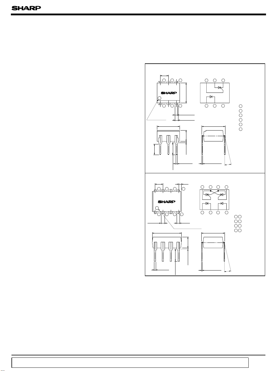
■ Outline Dimensions
S22MD1V
Anode
mark
0.5
±
3.35
S22MD3
2.54
±
0.25
2.54
S22MD1V
123
±
7.12
±
0.25
8
7
S22MD3
S22MD1V/S22MD3
()
Internal connection diagram
456
0.5
±
6.5
±
0.2
0.9
±
0.3
1.2
0.5
0.5
±
3.5
TYP.
0.5
0.5
±
0.1
0.5
±
3.7
Internal connection diagram
±
0.2
0.8
6
5
123
±
0.3
7.62
±
0.1
0.26
θ : 0 to 13˚
8
7
❈ Lead forming type (I type) and taping reel type (P type) of S22MD1V S22MD1VI/S22MD1P
(
Unit : mm
456
1 Anode
2 Cathode
3 NC
4 Cathode
5 Anode
6 Gate
θ
56
)
2
1
9.22
0.5
±
±
0.5
0.1
34
0.85
Anode mark
0.5
±
3.0
±
0.3
1.2
“ In the absence of confirmation by device specification sheets, SHARP takes no responsibility for any defects that occur in equipment using any of SHARP's devices, shown in catalogs,
data books, etc. Contact SHARP in order to obtain the latest version of the device specification sheets before using any SHARP's device.”
1234
±
0.3
0.5
±
3.5
TYP.
0.5
θ : 0 to 13˚
7.62
0.26
1 4 Anode
2 3 Cathode
θ
5 8 Gate
67 Anode/
Cathode
±
0.3
±
0.1
Page 2
S22MD1V/S22MD3
■ Absolute Maximum Ratings
Parameter Symbol
Input
Forward current I
Reverse voltage V
RMS ON-state current
∗1
Output
Peak one cycle surge current I
∗2
Repetitive peak OFF-state voltage
∗2
Repetitive peak reverse voltage V
∗3
Isolation voltage V
Operating temperature T
Storage temperature T
∗4
Soldering temperature T
∗1 50HZ, sine wave
= 20kΩ
∗2 R
G
∗3 40 to 60%RH, AC for 1 minute
∗4 For 10 seconds
■ Electro-optical Characteristics
Parameter Conditions
Input
Output
Transfer
characteristics
∗5 Applies only to S22MD1V
Forward voltage
Reverse current
Repetitive peak OFF-state current
∗5
Repetitive peak reverse current
ON-state voltage
Holding current
Critical rate of
rise of OFF-state voltage
Minimum trigger current
Isolation resistance
Turn-on time
S22MD1V
S22MD3
Symbol
V
F
I
R
I
DRM
I
RRM
V
T
I
H
dV/dt
I
FT
R
ISO
t
on
S22MD1V S22MD3
F
R
I
T
surge
V
DRM
RRM
iso
opr
stg
sol
5 000 2 500
-30 to +100 -30 to +100
-55 to +125 -40 to +125
IF= 30mA
=3V
V
R
= Rated, RG= 20kΩ
V
DRM
= Rated, RG= 20kΩ
V
RRM
= 200mA
I
T
= 6V, RG= 20kΩ
V
D
2
V
= 1/ Rated, RG= 20kΩ
DRM
VD= 6V, RL= 100Ω , RG= 20kΩ
DC500V, 40 to 60%RH
VD= 6V, RG= 20kΩ , RL= 100Ω , IF= 30mA
(
Ta = 25˚C
Rating
Unit
50 mA
6V
200
mA
rms
2A
600 V
600 - V
V
rms
˚C
˚C
260 ˚C
(
Ta= 25˚C
MIN. TYP. MAX. Unit
- 1.2 1.4 V
-5
--10
--10
--10
A
-6
A
-6
A
- 1.0 1.4 V
- 0.2 1 mA
5-3-
-10mA
5x10
-
10
11
10
V/µs
-
- Ω
− 20 50 µs
)
)
Page 3

S22MD1V/S22MD3
Fig. 1 RMS ON-state Current vs.
Ambient Temperature
)
200
mARMS ON-state current I
(
T rms
100
0
-
30 0 20406080100
Ambient temperature Ta (˚C
)
Fig. 3 Forward Current vs. Forward Voltage
500
= 75˚C
T
a
200
)
100
mA
(
F
50
20
10
Forward current I
5
2
1
0 0.5 1.0 1.5 2.0 2.5 3.0
50˚C
Forward voltage VF (V
25˚C
0˚C
- 25˚C
)
Fig. 2 Forward Current vs.
Ambient Temperature
70
60
)
50
mA
(
F
40
30
20
Forward current I
10
0
-
30 0 25 50 75 100 125
Ambient temperature Ta (˚C
Fig. 4 Minimum Trigger Current vs.
Ambient Temperature
12
V
=6V
D
R
= 100Ω
L
)
10
mA
(
FT
8
6
4
Minimum trigger current I
2
0
-
30 0 20406080100
Ambient temperature T
RG= 10kΩ
(˚C
a
)
20kΩ
50kΩ
)
Fig. 5 Minimum Trigger Current vs.
Gate Resistance
100
50
)
mA
(
FT
20
10
5
Minimum trigger current I
2
1
1 2 5 10 20 50 100 200
Gate resistance R
G
(kΩ
Fig. 6 Break Over Voltage vs.
Ambient Temperature
V
=6V
D
R
= 100Ω
L
= 25˚C
T
a
)
900
800
)
700
V
(
600
BO
500
400
300
Break over voltage V
200
100
0
-30-
20 0 20 40 60 80 100 120
Ambient temperature Ta (˚C
20kΩ
R
G
= 10kΩ
50kΩ
)
Page 4

S22MD1V/S22MD3
Fig. 7 Critical Rate of Rise of OFF-state
Voltage vs. Ambient Temperature
100
50
R
V
DRM
= 20kΩ
G
= 1/ Rated
2
20
10
)
5
V/µ s
(
2
dV/dt
Critical rate of rise of OFF-state voltage
1
0 20406080100
Ambient temperature Ta (˚C
)
Fig. 9 Repetitive Peak OFF-state Current vs.
Ambient Temperature
5
V
)
A
2
(
-6
10
DRM
5
2
-7
10
5
2
-8
10
5
Repetitive peak OFF-state current I
2
0 20406080100
= Rated
DRM
R
= 20kΩ
G
Ambient temperature Ta (˚C
)
Fig. 8 Holding Current vs.
Ambient Temperature
1
0.5
)
mA
(
0.2
H
0.1
0.05
Holding current I
0.02
0.01
-
30 0 20406080100
Ambient temperature Ta (˚C
20kΩ
50kΩ
V
R
)
D
G
=6V
= 10kΩ
Page 5

■ Basic Operation Circuit
● S22MD1V
Medium/High Power Thyristor Drive Circuit
S22MD1V/S22MD3
+V
CC
V
IN
16
2
3
5
C
G
4
R
G
Medium/High Power Triac Drive Circuit (Zero-cross Operation
+ V
CC
V
IN
16
2
3
5
R
G
C
G
4
● S22MD3
Low Power Load Drive Circuit
8
7
C
G
R
G
R
G
6
5
+ V
CC
1
2
3
V
IN
4
Load
Z
S
Z
: Snubber circuit
S
AC 100V, 200V
)
Load
AC 100V, 200V
Load
C
G
Z
S
Z
: Snubber circuit
S
AC 100V, 200V
Medium/High Power Triac Drive Circuit
+ V
CC
1
2
3
V
IN
●
Please refer to the chapter “Precautions for Use”(Page 78 to 93).
4
8
7
C
G
R
6
G
C
G
R
G
5
Load
AC 100V, 200V
 Loading...